

Texas Instruments SN74AHCT158D, SN74AHCT158DBLE, SN74AHCT158DBR, SN74AHCT158DGVR, SN74AHCT158DR Datasheet
...
SN54AHCT158, SN74AHCT158
QUADRUPLE 2-LINE TO 1-LINE DATA SELECTORS/MULTIPLEXERS
SCLS348H – MAY 1996 – REVISED JANUAR Y 2000
1
POST OFFICE BOX 655303 • DALLAS, TEXAS 75265
D
EPIC
(Enhanced-Performance Implanted
CMOS) Process
D
Inputs Are TTL-Voltage Compatible
D
Latch-Up Performance Exceeds 250 mA Per
JESD 17
D
ESD Protection Exceeds 2000 V Per
MIL-STD-833, Method 3015; Exceeds 200 V
Using Machine Model (C = 200 pF, R = 0)
D
Package Options Include Plastic
Small-Outline (D), Shrink Small-Outline
(DB), Thin Very Small-Outline (DGV), Thin
Shrink Small-Outline (PW), and Ceramic
Flat (W) Packages, Ceramic Chip Carriers
(FK), and Standard Plastic (N) and Ceramic
(J) DIPs
description
These quadruple 2-line to 1-line data
selectors/multiplexers are designed for 4.5-V to
5.5-V V
CC
operation.
The ’AHCT158 devices feature a common strobe
(G
) input. When the strobe is high, all outputs are
high. When the strobe is low, a 4-bit word is
selected from one of two sources and is routed to
the four outputs. The devices provide inverted
data.
The SN54AHCT158 is characterized for
operation over the full military temperature range
of –55°C to 125°C. The SN74AHCT158 is
characterized for operation from –40°C to 85°C.
FUNCTION TABLE
(each data selector/multiplexer)
INPUTS
OUTPUT
G A/B A B
Y
H X X X H
L LLX H
L LHX L
L HXL H
L H X H L
Copyright 2000, Texas Instruments Incorporated
UNLESS OTHERWISE NOTED this document contains PRODUCTION
DATA information current as of publication date. Products conform to
specifications per the terms of Texas Instruments standard warranty.
Production processing does not necessarily include testing of all
parameters.
Please be aware that an important notice concerning availability, standard warranty, and use in critical applications of
Texas Instruments semiconductor products and disclaimers thereto appears at the end of this data sheet.
EPIC is a trademark of Texas Instruments Incorporated.
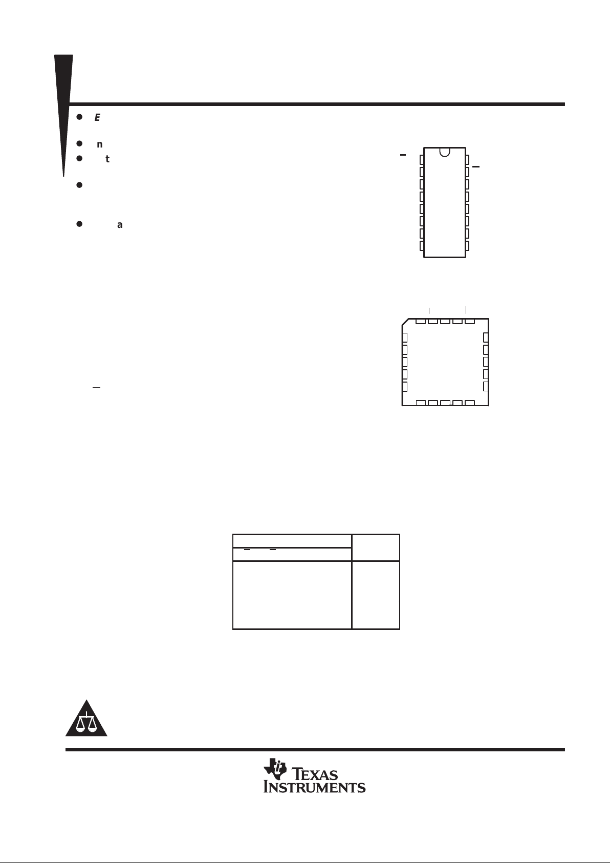
SN54AHCT158 ...J OR W PACKAGE
SN74AHCT158 . . . D, DB, DGV, N, OR PW PACKAGE
(TOP VIEW)
3212019
910111213
4
5
6
7
8
18
17
16
15
14
4A
4B
NC
4Y
3A
1B
1Y
NC
2A
2B
SN54AHCT158 . . . FK PACKAGE
(TOP VIEW)
1A
A/B
NC
3Y
3B
V
G
2Y
GND
NC
CC
1
2
3
4
5
6
7
8
16
15
14
13
12
11
10
9
A/B
1A
1B
1Y
2A
2B
2Y
GND
V
CC
G
4A
4B
4Y
3A
3B
3Y
NC – No internal connection
SN54AHCT158, SN74AHCT158
QUADRUPLE 2-LINE TO 1-LINE DATA SELECTORS/MULTIPLEXERS
SCLS348H – MAY 1996 – REVISED JANUAR Y 2000
2
POST OFFICE BOX 655303 • DALLAS, TEXAS 75265
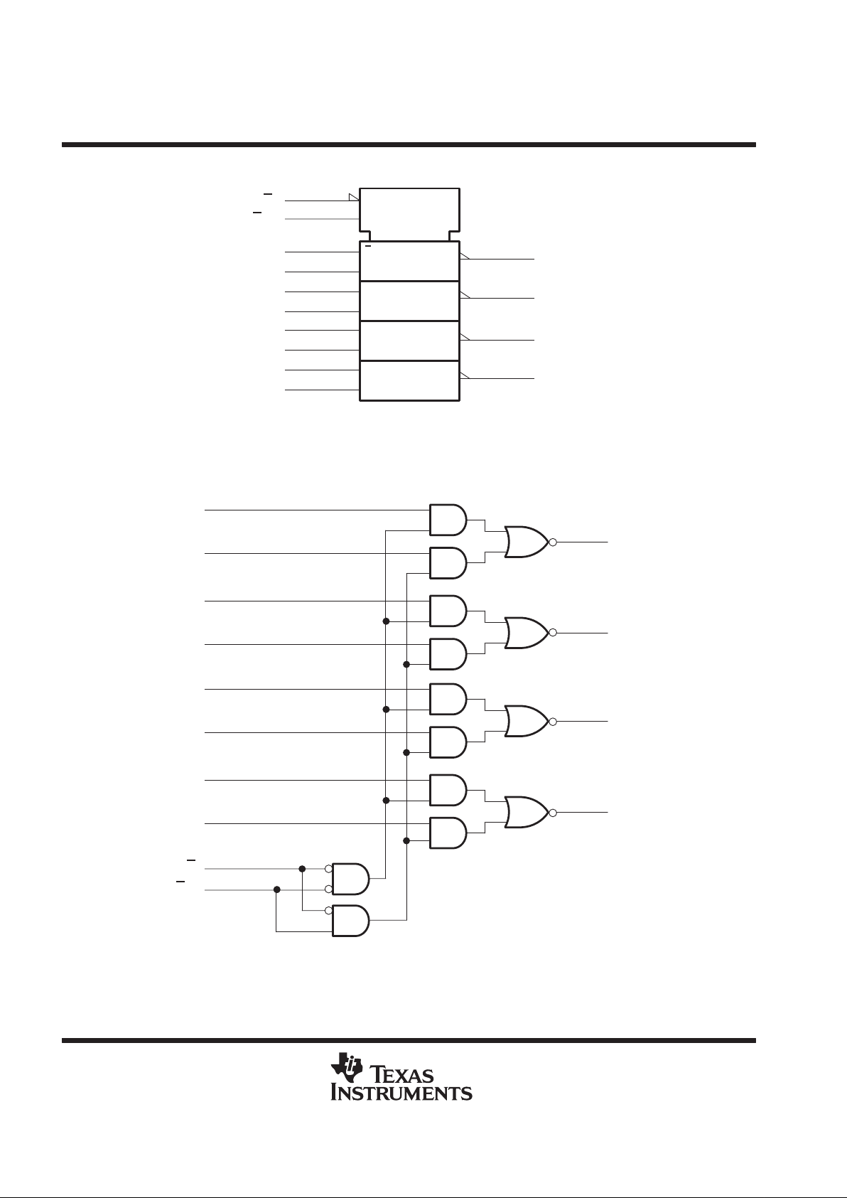
logic symbol
†
2
1A
1
3
1B
5
2A
6
2B
11
3A
10
3B
14
4A
13
4B
EN
15
G1
1
MUX
1
1Y
4
2Y
7
3Y
9
4Y
12
G
A/B
†
This symbol is in accordance with ANSI/IEEE Std 91-1984 and IEC Publication 617-12.
Pin numbers shown are for the D, DB, DGV , J, N, PW, and W packages.
logic diagram (positive logic)
2
3
5
6
11
10
14
13
15
1
G
A/B
4B
4A
3B
3A
2B
2A
1B
1A
4
7
9
12
1Y
2Y
3Y
4Y
Pin numbers shown are for the D, DB, DGV, J, N, PW, and W packages.
SN54AHCT158, SN74AHCT158
QUADRUPLE 2-LINE TO 1-LINE DATA SELECTORS/MULTIPLEXERS
SCLS348H – MAY 1996 – REVISED JANUAR Y 2000
3
POST OFFICE BOX 655303 • DALLAS, TEXAS 75265
absolute maximum ratings over operating free-air temperature range (unless otherwise noted)
†
Supply voltage range, VCC –0.5 V to 7 V. . . . . . . . . . . . . . . . . . . . . . . . . . . . . . . . . . . . . . . . . . . . . . . . . . . . . . . . . .
Input voltage range, VI (see Note 1) –0.5 V to 7 V. . . . . . . . . . . . . . . . . . . . . . . . . . . . . . . . . . . . . . . . . . . . . . . . . .
Output voltage range, V
O
(see Note 1) –0.5 V to VCC + 0.5 V. . . . . . . . . . . . . . . . . . . . . . . . . . . . . . . . . . . . . . . .
Input clamp current, IIK (VI < 0) –20 mA. . . . . . . . . . . . . . . . . . . . . . . . . . . . . . . . . . . . . . . . . . . . . . . . . . . . . . . . . . .
Output clamp current, IOK (VO < 0 or VO > VCC) ±20 mA. . . . . . . . . . . . . . . . . . . . . . . . . . . . . . . . . . . . . . . . . . . .
Continuous output current, IO (VO = 0 to VCC) ±25 mA. . . . . . . . . . . . . . . . . . . . . . . . . . . . . . . . . . . . . . . . . . . . . .
Continuous current through VCC or GND ±50 mA. . . . . . . . . . . . . . . . . . . . . . . . . . . . . . . . . . . . . . . . . . . . . . . . . . .
Package thermal impedance, θ
JA
(see Note 2): D package 73°C/W. . . . . . . . . . . . . . . . . . . . . . . . . . . . . . . . . . .
DB package 82°C/W. . . . . . . . . . . . . . . . . . . . . . . . . . . . . . . . .
DGV package 120°C/W. . . . . . . . . . . . . . . . . . . . . . . . . . . . . . .
N package 67°C/W. . . . . . . . . . . . . . . . . . . . . . . . . . . . . . . . . . .
PW package 108°C/W. . . . . . . . . . . . . . . . . . . . . . . . . . . . . . . .
Storage temperature range, T
stg
–65°C to 150°C. . . . . . . . . . . . . . . . . . . . . . . . . . . . . . . . . . . . . . . . . . . . . . . . . . .
†
Stresses beyond those listed under “absolute maximum ratings” may cause permanent damage to the device. These are stress ratings only, and
functional operation of the device at these or any other conditions beyond those indicated under “recommended operating conditions” is not
implied. Exposure to absolute-maximum-rated conditions for extended periods may affect device reliability.
NOTES: 1. The input and output voltage ratings may be exceeded if the input and output current ratings are observed.
2. The package thermal impedance is calculated in accordance with JESD 51.
recommended operating conditions (see Note 3)
SN54AHCT158 SN74AHCT158
MIN MAX MIN MAX
UNIT
V
CC
Supply voltage 4.5 5.5 4.5 5.5 V
V
IH
High-level input voltage 2 2 V
V
IL
Low-level input voltage 0.8 0.8 V
V
I
Input voltage 0 5.5 0 5.5 V
V
O
Output voltage 0 V
CC
0 V
CC
V
I
OH
High-level output current –8 –8 mA
I
OL
Low-level output current 8 8 mA
∆t/∆v Input transition rise or fall time 20 20 ns/V
T
A
Operating free-air temperature –55 125 –40 85 °C
NOTE 3: All unused inputs of the device must be held at VCC or GND to ensure proper device operation. Refer to the TI application report,
Implications of Slow or Floating CMOS Inputs
, literature number SCBA004.
PRODUCT PREVIEW information concerns products in the formative or
design phase of development. Characteristic data and other
specifications are design goals. Texas Instruments reserves the right to
change or discontinue these products without notice.
 Loading...