

Texas Instruments SN74AHC594DBR, SN74AHC594DR, SN74AHC594N, SN74AHC594NSR, SN74AHC594PWR Datasheet
...
SN54AHC594, SN74AHC594
8-BIT SHIFT REGISTERS
WITH OUTPUT REGISTERS
SCLS423C – JUNE 1998 – REVISED JANUARY 2000
D
EPIC
(Enhanced-Performance
Implanted CMOS) Process
D
Operating Range 2-V to 5.5-V V
D
8-Bit Serial-In, Parallel-Out Shift
CC
Registers With Storage
D
Independent Direct Overriding Clears
on Shift and Storage Registers
D
Independent Clocks for Shift and
Storage Registers
D
Latch-Up Performance Exceeds 100 mA
Per JESD 78, Class II
D
ESD Protection Exceeds JESD 22
– 2000-V Human-Body Model (A114-A)
– 200-V Machine Model (A115-A)
– 1000-V Charged-Device Model (C101)
D
Package Options Include Plastic
Small-Outline (D), Shrink Small-Outline
(DB), Thin Shrink Small-Outline (PW),
and Ceramic Flat (W) Packages,
Ceramic Chip Carriers (FK), and
Standard Plastic (N) and Ceramic (J)
DIPs
description
The ’AHC594 devices contain an 8-bit serial-in,
parallel-out shift register that feeds an 8-bit D-type
storage register. Separate clocks and direct
overriding clear (SRCLR, RCLR) inputs are
provided on the shift and storage registers. A
serial (Q
purposes.
) output is provided for cascading
H′
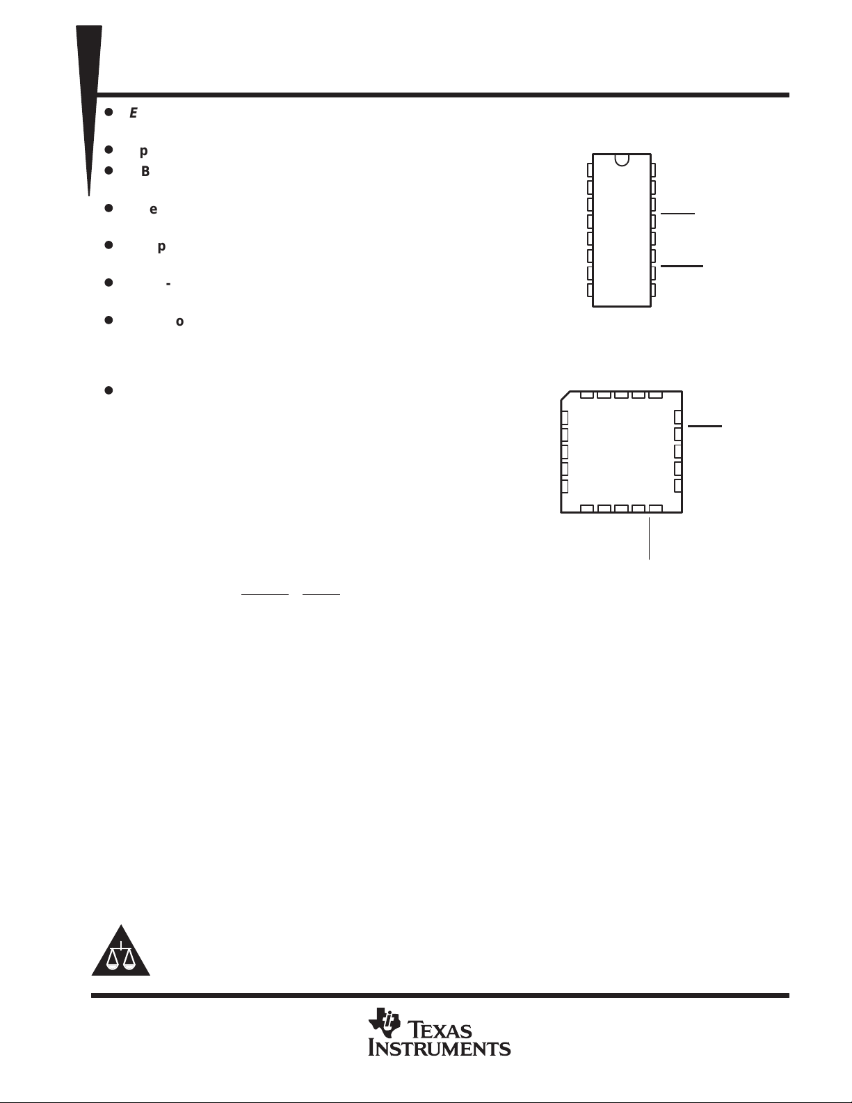
SN54AHC594 ...J OR W PACKAGE
SN74AHC594 . . . D, DB, N, OR PW PACKAGE
SN54AHC594 . . . FK PACKAGE
Q
D
Q
E
NC
Q
F
Q
G
NC – No internal connection
(TOP VIEW)
Q
1
B
Q
2
C
Q
3
D
Q
4
E
5
Q
F
6
Q
G
7
Q
H
GND
8
(TOP VIEW)
CQB
Q
3212019
4
5
6
7
8
910111213
H
Q
NC
NC
GND
16
15
14
13
12
11
10
9
VCCQ
′
H
Q
V
CC
Q
A
SER
RCLR
RCLK
SRCLK
SRCLR
Q
H′
A
SER
18
RCLR
17
NC
16
RCLK
15
14
SRCLK
SRCLR
The shift register (SRCLK) and storage register (RCLK) clocks are positive-edge triggered. If the clocks are tied
together, the shift register always is one clock pulse ahead of the storage register.
The SN54AHC594 is characterized for operation over the full military temperature range of –55°C to 125°C. The
SN74AHC594 is characterized for operation from –40°C to 85°C.
Please be aware that an important notice concerning availability, standard warranty, and use in critical applications of
Texas Instruments semiconductor products and disclaimers thereto appears at the end of this data sheet.
EPIC is a trademark of Texas Instruments Incorporated.
UNLESS OTHERWISE NOTED this document contains PRODUCTION
DATA information current as of publication date. Products conform to
specifications per the terms of Texas Instruments standard warranty.
Production processing does not necessarily include testing of all
parameters.
POST OFFICE BOX 655303 • DALLAS, TEXAS 75265
Copyright 2000, Texas Instruments Incorporated
1
SN54AHC594, SN74AHC594
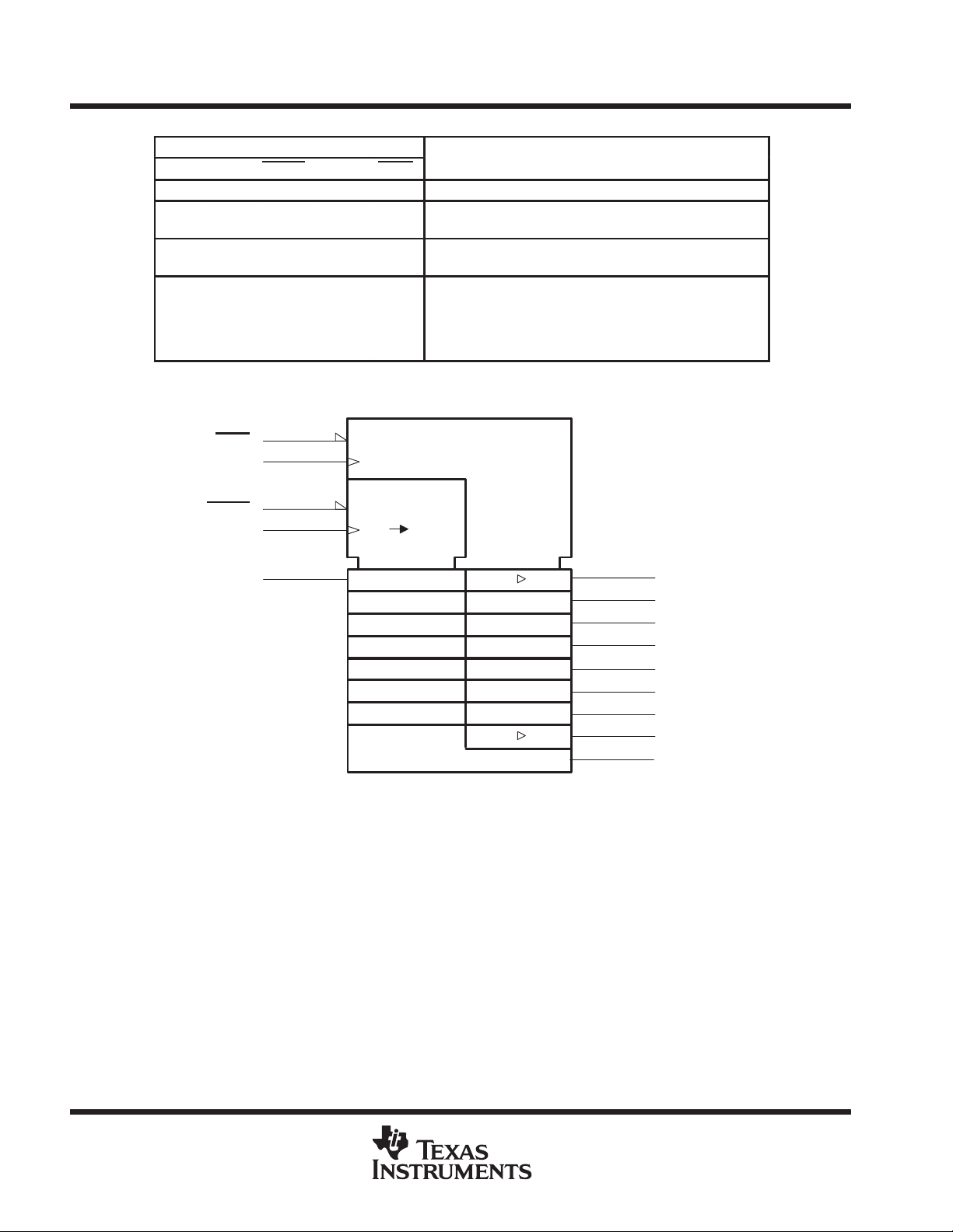
FUNCTION
8-BIT SHIFT REGISTERS
WITH OUTPUT REGISTERS
SCLS423C – JUNE 1998 – REVISED JANUARY 2000
INPUTS
SER SRCLK SRCLR RCLK RCLR
X X L X X Shift register is cleared.
L ↑ H X X
H ↑ H X X
L ↓ H X X Shift register state is not changed.
X X X X L Storage register is cleared.
X XX↑ H Shift register data is stored in the storage register.
X X X ↓ H Storage register state is not changed.
FUNCTION TABLE
First stage of shift register goes low.
Other stages store the data of previous stage, respectively.
First stage of shift register goes high.
Other stages store the data of previous stage, respectively.
logic symbol
†
This symbol is in accordance with ANSI/IEEE Std 91-1984 and IEC Publication 617-12.
Pin numbers shown are for the D, DB, J, N, PW, and W packages.
†
SER
13
12
10
11
14
RCLR
RCLK C2
SRCLR
SRCLK C1/
R3
R
1D
SRG8
2D
2D
15
3
3
Q
A
1
Q
B
2
Q
C
3
Q
D
4
Q
E
5
Q
F
6
Q
G
7
Q
H
9
Q
H′
2
POST OFFICE BOX 655303 • DALLAS, TEXAS 75265
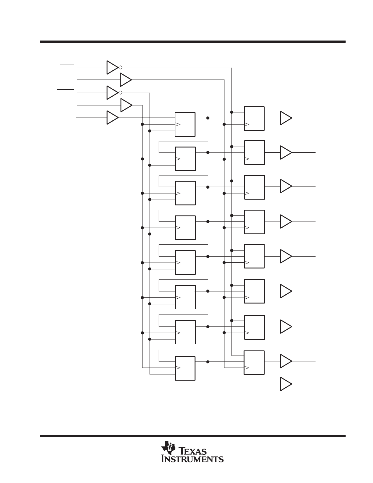
logic diagram (positive logic)
SN54AHC594, SN74AHC594
8-BIT SHIFT REGISTERS
WITH OUTPUT REGISTERS
SCLS423C – JUNE 1998 – REVISED JANUARY 2000
RCLR
RCLK
SRCLR
SRCLK
SER
13
12
10
11
14 15
1D
R
2D
R
2D
R
2D
R
Q
C1
Q
C2
Q
C2
Q
C2
R
3D
R
3D
R
3D
R
3D
Q
C3
Q
C3
Q
C3
Q
C3
Q
A
1
Q
B
2
Q
C
3
Q
D
2D
R
2D
R
2D
R
2D
R
Pin numbers shown are for the D, DB, J, N, PW, and W packages.
C2
C2
C2
C2
Q
Q
Q
Q
R
3D
R
3D
R
3D
R
3D
Q
C3
Q
C3
Q
C3
Q
C3
4
Q
E
5
Q
F
6
Q
G
7
Q
H
9
Q
H′
POST OFFICE BOX 655303 • DALLAS, TEXAS 75265
3
 Loading...