

Datasheet SN74AHC139D, SN74AHC139DBLE, SN74AHC139DBR, SN74AHC139DGVR, SN74AHC139DR Datasheet (Texas Instruments)
...
SN54AHC139, SN74AHC139
DUAL 2-LINE TO 4-LINE DECODERS/DEMULTIPLEXERS
SCLS259H – DECEMBER 1995 – REVISED JANUARY 2000
D
EPIC
(Enhanced-Performance Implanted
CMOS) Process
D
Operating Range 2-V to 5.5-V V
D
Designed Specifically for High-Speed
CC
Memory Decoders and Data-Transmission
Systems
D
Incorporate Two Enable Inputs to Simplify
Cascading and/or Data Reception
D
Latch-Up Performance Exceeds 250 mA Per
JESD 17
D
ESD Protection Exceeds 2000 V Per
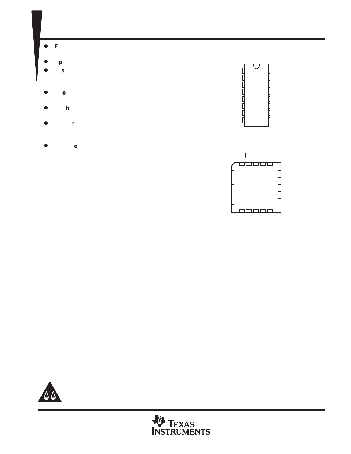
SN54AHC139 ...J OR W PACKAGE
SN74AHC139 . . . D, DB, DGV, N, OR PW PACKAGE
1G
1A
1B
1Y0
1Y1
1Y2
1Y3
GND
(TOP VIEW)
1
16
2
15
3
14
4
13
5
12
6
11
7
10
8
V
CC
2G
2A
2B
2Y0
2Y1
2Y2
9
2Y3
MIL-STD-883, Method 3015; Exceeds 200 V
Using Machine Model (C = 200 pF, R = 0)
D
Package Options Include Plastic
Small-Outline (D), Shrink Small-Outline
(DB), Thin Very Small-Outline (DGV), Thin
Shrink Small-Outline (PW), and Ceramic
Flat (W) Packages, Ceramic Chip Carriers
(FK), and Standard Plastic (N) and Ceramic
(J) DIPs
description
SN54AHC139 . . . FK PACKAGE
1B
1Y0
NC
1Y1
1Y2
(TOP VIEW)
1A1GNC
3212019
4
5
6
7
8
910111213
V
CC
2G
18
17
16
15
14
2A
2B
NC
2Y0
2Y1
The ’AHC139 devices are dual 2-line to 4-line
decoders/demultiplexers designed for 2-V to
5.5-V V
operation. These devices are
CC
designed to be used in high-performance
NC – No internal connection
1Y3
NC
GND
2Y3
2Y2
memory-decoding or data-routing applications
requiring very short propagation delay times. In
high-performance memory systems, these decoders can be used to minimize the effects of system decoding.
When used with high-speed memories utilizing a fast enable circuit, the delay times of these decoders and the
enable time of the memory usually are less than the typical access time of the memory. This means that the
effective system delay introduced by the decoders is negligible.
The active-low enable (G
) input can be used as a data line in demultiplexing applications. These
decoders/demultiplexers feature fully buffered inputs, each of which represents only one normalized load to its
driving circuit.
The SN54AHC139 is characterized for operation over the full military temperature range of –55°C to 125°C. The
SN74AHC139 is characterized for operation from –40°C to 85°C.
Please be aware that an important notice concerning availability, standard warranty, and use in critical applications of
Texas Instruments semiconductor products and disclaimers thereto appears at the end of this data sheet.
EPIC is a trademark of Texas Instruments Incorporated.
UNLESS OTHERWISE NOTED this document contains PRODUCTION
DATA information current as of publication date. Products conform to
specifications per the terms of Texas Instruments standard warranty.
Production processing does not necessarily include testing of all
parameters.
POST OFFICE BOX 655303 • DALLAS, TEXAS 75265
Copyright 2000, Texas Instruments Incorporated
1
SN54AHC139, SN74AHC139
OUTPUTS
G
DUAL 2-LINE TO 4-LINE DECODERS/DEMULTIPLEXERS
SCLS259H – DECEMBER 1995 – REVISED JANUARY 2000
FUNCTION TABLE
(each decoder/demultiplexer)
INPUTS
SELECT
B A Y0 Y1 Y2 Y3
H X X H H H H
L L LLHHH
L L HHLHH
L H LHHLH
L H H H H H L
X/Y
†
4
12
11
10
1Y0
5
1Y1
6
1Y2
7
1Y3
2Y0
2Y1
2Y2
9
2Y3
0
1
2
3
1A
1B
1G
2A
2B
2G
2
3
1
14
13
15
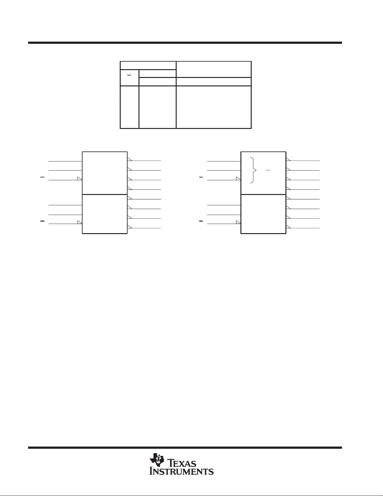
logic symbols (alternatives)
2
1A
3
1B
1
1G
14
2A
13
2B
15
2G
†
These symbols are in accordance with ANSI/IEEE Std 91-1984 and IEC Publication 617-12.
Pin numbers shown are for the D, DB, DGV, J, N, PW, and W packages.
1
2
EN
EN
1
2
EN
EN
DMUX
G
4
12
11
10
1Y0
5
1Y1
6
1Y2
7
1Y3
2Y0
2Y1
2Y2
9
2Y3
0
0
1
3
2
3
2
POST OFFICE BOX 655303 • DALLAS, TEXAS 75265
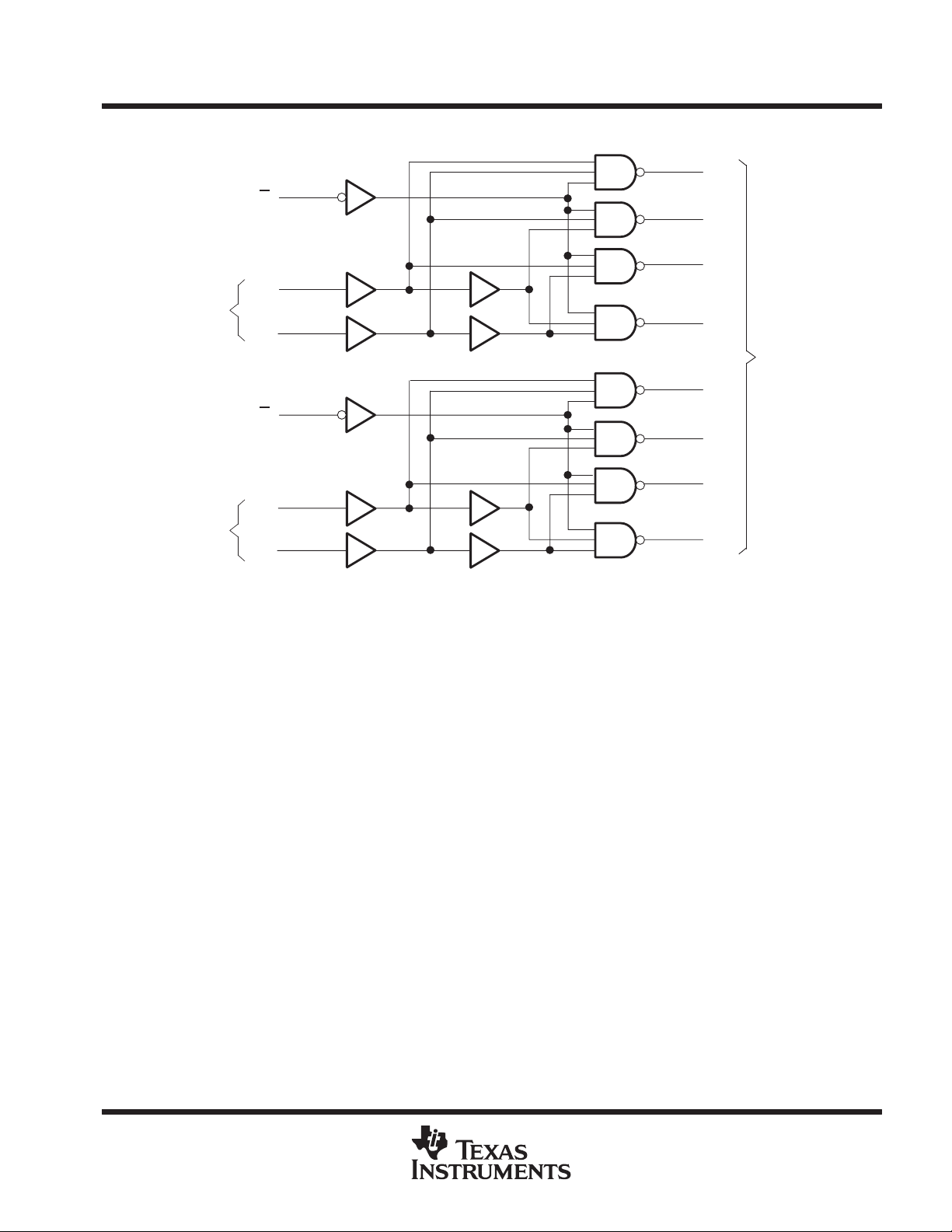
logic diagram (positive logic)
1
1G
2
Select
Inputs
Select
Inputs
1A
1B
2G
2A
2B
3
15
14
13
SN54AHC139, SN74AHC139
DUAL 2-LINE TO 4-LINE DECODERS/DEMULTIPLEXERS
SCLS259H – DECEMBER 1995 – REVISED JANUARY 2000
4
1Y0
5
1Y1
6
1Y2
7
1Y3
Data
12
11
10
2Y0
2Y1
2Y2
9
2Y3
Outputs
Pin numbers shown are for the D, DB, DGV, J, N, PW, and W packages.
absolute maximum ratings over operating free-air temperature range (unless otherwise noted)
Supply voltage range, VCC –0.5 V to 7 V. . . . . . . . . . . . . . . . . . . . . . . . . . . . . . . . . . . . . . . . . . . . . . . . . . . . . . . . . .
Input voltage range, VI (see Note 1) –0.5 V to 7 V. . . . . . . . . . . . . . . . . . . . . . . . . . . . . . . . . . . . . . . . . . . . . . . . . .
Output voltage range, V
Input clamp current, I
Output clamp current, I
Continuous output current, I
(see Note 1) –0.5 V to V
O
(V
< 0) –20 mA. . . . . . . . . . . . . . . . . . . . . . . . . . . . . . . . . . . . . . . . . . . . . . . . . . . . . . . . . . .
IK
I
(V
< 0 or VO > VCC) ±20 mA. . . . . . . . . . . . . . . . . . . . . . . . . . . . . . . . . . . . . . . . . . . .
OK
O
(V
= 0 to VCC) ±25 mA. . . . . . . . . . . . . . . . . . . . . . . . . . . . . . . . . . . . . . . . . . . . . .
O
O
Continuous current through VCC or GND ±75 mA. . . . . . . . . . . . . . . . . . . . . . . . . . . . . . . . . . . . . . . . . . . . . . . . . . .
Package thermal impedance, θ
(see Note 2): D package 73°C/W. . . . . . . . . . . . . . . . . . . . . . . . . . . . . . . . . . .
JA
DB package 82°C/W. . . . . . . . . . . . . . . . . . . . . . . . . . . . . . . . .
DGV package 120°C/W. . . . . . . . . . . . . . . . . . . . . . . . . . . . . . .
N package 67°C/W. . . . . . . . . . . . . . . . . . . . . . . . . . . . . . . . . . .
PW package 108°C/W. . . . . . . . . . . . . . . . . . . . . . . . . . . . . . . .
Storage temperature range, T
†
Stresses beyond those listed under “absolute maximum ratings” may cause permanent damage to the device. These are stress ratings only, and
functional operation of the device at these or any other conditions beyond those indicated under “recommended operating conditions” is not
implied. Exposure to absolute-maximum-rated conditions for extended periods may affect device reliability.
NOTES: 1. The input and output voltage ratings may be exceeded if the input and output current ratings are observed.
2. The package thermal impedance is calculated in accordance with JESD 51.
–65°C to 150°C. . . . . . . . . . . . . . . . . . . . . . . . . . . . . . . . . . . . . . . . . . . . . . . . . . .
stg
CC
+ 0.5 V. . . . . . . . . . . . . . . . . . . . . . . . . . . . . . . . . . . . . . . .
†
POST OFFICE BOX 655303 • DALLAS, TEXAS 75265
3

SN54AHC139, SN74AHC139
UNIT
mA
mA
∆t/∆vInput transition rise or fall rate
ns/V
PARAMETER
TEST CONDITIONS
V
UNIT
OH
OL
DUAL 2-LINE TO 4-LINE DECODERS/DEMULTIPLEXERS
SCLS259H – DECEMBER 1995 – REVISED JANUARY 2000
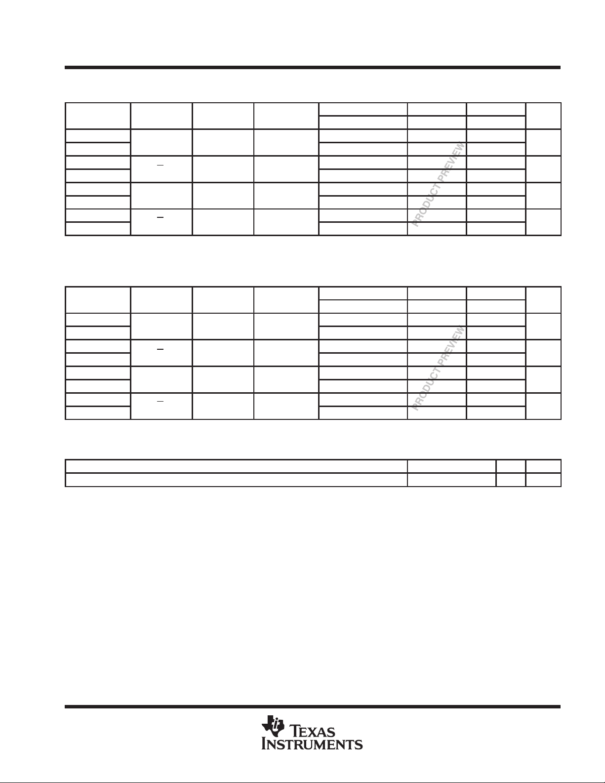
recommended operating conditions (see Note 3)
SN54AHC139 SN74AHC139
MIN MAX MIN MAX
V
V
V
V
V
I
OH
I
OL
T
NOTE 3: All unused inputs of the device must be held at VCC or GND to ensure proper device operation. Refer to the TI application report,
Supply voltage 2 5.5 2 5.5 V
CC
VCC = 2 V 1.5 1.5
High-level input voltage
IH
Low-level input voltage
IL
Input voltage 0 5.5 0 5.5 V
I
Output voltage 0 V
O
High-level output current
Low-level output current
p
Operating free-air temperature –55 125 –40 85 °C
A
Implications of Slow or Floating CMOS Inputs
, literature number SCBA004.
VCC = 3 V
VCC = 5.5 V 3.85 3.85
VCC = 2 V 0.5 0.5
VCC = 3 V
VCC = 5.5 V 1.65 1.65
VCC = 2 V –50 –50
VCC = 3.3 V ± 0.3 V
VCC = 5 V ± 0.5 V –8 –8
VCC = 2 V 50 50
VCC = 3.3 V ± 0.3 V
VCC = 5 V ± 0.5 V 8 8
VCC = 3.3 V ± 0.3 V 100 100
VCC = 5 V ± 0.5 V 20 20
2.1 2.1
0.9 0.9
CC
–4 –4
4 4
0 V
CC
V
V
V
m
A
m
A
electrical characteristics over recommended operating free-air temperature range (unless
otherwise noted)
CC
2 V 1.9 2 1.9 1.9
IOH = –50 mA
V
OH
IOH = –4 mA
IOH = –8 mA
IOL = 50 mA
V
OL
IOL = 4 mA
IOL = 8 mA
I
I
I
CC
C
i
* On products compliant to MIL-PRF-38535, this parameter is not production tested at VCC = 0 V.
VI = VCC or GND 0 V to 5.5 V ±0.1 ±1* ±1
VI = VCC or GND, IO = 0 5.5 V 4 40 40
VI = VCC or GND 5 V 2 10 10 pF
3 V 2.9 3 2.9 2.9
4.5 V 4.4 4.5 4.4 4.4
3 V 2.58 2.48 2.48
4.5 V 3.94 3.8 3.8
2 V 0.1 0.1 0.1
3 V 0.1 0.1 0.1
4.5 V 0.1 0.1 0.1
3 V 0.36 0.5 0.44
4.5 V 0.36 0.5 0.44
TA = 25°C SN54AHC139 SN74AHC139
MIN TYP MAX MIN MAX MIN MAX
V
V
m
A
m
A
PRODUCT PREVIEW information concerns products in the formative or
design phase of development. Characteristic data and other
specifications are design goals. Texas Instruments reserves the right to
change or discontinue these products without notice.
4
POST OFFICE BOX 655303 • DALLAS, TEXAS 75265
PARAMETER
UNIT
A or B
Y
C
15 pF
ns
G
Y
C
15 pF
ns
A or B
Y
C
pF
ns
G
Y
C
50 pF
ns
PARAMETER
UNIT
A or B
Y
C
pF
ns
G
Y
C
pF
ns
A or B
Y
C
pF
ns
G
Y
C
pF
ns
SN54AHC139, SN74AHC139
DUAL 2-LINE TO 4-LINE DECODERS/DEMULTIPLEXERS
SCLS259H – DECEMBER 1995 – REVISED JANUARY 2000
switching characteristics over recommended operating free-air temperature range,
V
= 3.3 V ± 0.3 V (unless otherwise noted) (see Figure 1)
CC
FROM TO LOAD
(INPUT) (OUTPUT) CAPACITANCE
t
PLH
t
PHL
t
PLH
t
PHL
t
PLH
t
PHL
t
PLH
t
PHL
* On products compliant to MIL-PRF-38535, this parameter is not production tested.
=
L
=
L
= 50
L
=
L
p
p
p
p
switching characteristics over recommended operating free-air temperature range,
V
= 5 V ± 0.5 V (unless otherwise noted) (see Figure 1)
CC
FROM TO LOAD
(INPUT) (OUTPUT) CAPACITANCE
t
PLH
t
PHL
t
PLH
t
PHL
t
PLH
t
PHL
t
PLH
t
PHL
*
On products compliant to MIL-PRF-38535, this parameter is not production tested.
= 15
L
= 15
L
= 50
L
= 50
L
p
p
p
p
TA = 25°C SN54AHC139 SN74AHC139
MIN TYP MAX MIN MAX MIN MAX
7.2* 11* 1* 13* 1 13
7.2* 11* 1* 13* 1 13
6.4* 9.2* 1* 11* 1 11
6.4* 9.2* 1* 11* 1 11
9.7 14.5 1 16.5 1 16.5
9.7 14.5 1 16.5 1 16.5
8.9 12.7 1 14.5 1 14.5
8.9 12.7 1 14.5 1 14.5
TA = 25°C SN54AHC139 SN74AHC139
MIN TYP MAX MIN MAX MIN MAX
5* 7.2* 1* 8.5* 1 8.5
5* 7.2* 1* 8.5* 1 8.5
4.4* 6.3* 1* 7.5* 1 7.5
4.4* 6.3* 1* 7.5* 1 7.5
6.5 9.2 1 10.5 1 10.5
6.5 9.2 1 10.5 1 10.5
5.9 8.3 1 9.5 1 9.5
5.9 8.3 1 9.5 1 9.5
operating characteristics, V
C
Power dissipation capacitance No load, f = 1 MHz 13 pF
pd
PRODUCT PREVIEW information concerns products in the formative or
design phase of development. Characteristic data and other
specifications are design goals. Texas Instruments reserves the right to
change or discontinue these products without notice.
CC
PARAMETER TEST CONDITIONS TYP UNIT
= 5 V, T
= 25°C
A
POST OFFICE BOX 655303 • DALLAS, TEXAS 75265
5
SN54AHC139, SN74AHC139
DUAL 2-LINE TO 4-LINE DECODERS/DEMULTIPLEXERS
SCLS259H – DECEMBER 1995 – REVISED JANUARY 2000
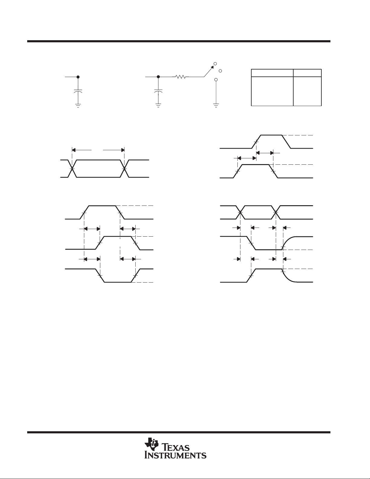
PARAMETER MEASUREMENT INFORMATION
From Output
Under Test
(see Note A)
Test
Point
C
L
From Output
Under Test
(see Note A)
C
L
RL = 1 kΩ
S1
V
CC
GND
Open
TEST S1
t
PLH/tPHL
t
PLZ/tPZL
t
PHZ/tPZH
Open Drain
Open
V
CC
GND
V
CC
LOAD CIRCUIT FOR
TOTEM-POLE OUTPUTS
Input
Input
t
PLH
In-Phase
Output
t
PHL
Out-of-Phase
Output
PROPAGATION DELAY TIMES
INVERTING AND NONINVERTING OUTPUTS
t
w
50% V
CC
VOLTAGE WAVEFORMS
PULSE DURATION
50% V
CC
50% V
50% V
VOLTAGE WAVEFORMS
50% V
CC
CC
3-STATE AND OPEN-DRAIN OUTPUTS
50% V
LOAD CIRCUIT FOR
V
CC
CC
0 V
V
CC
CC
t
PHL
50% V
t
PLH
50% V
CC
CC
0 V
V
V
V
V
OH
OL
OH
OL
Timing Input
Data Input
Output
Control
Output
Waveform 1
S1 at V
(see Note B)
Output
Waveform 2
S1 at GND
(see Note B)
50% V
t
su
50% V
CC
VOLTAGE WAVEFORMS
SETUP AND HOLD TIMES
50% V
CC
t
PZL
50% V
50% V
CC
CC
CC
t
PZH
VOLTAGE WAVEFORMS
ENABLE AND DISABLE TIMES
LOW- AND HIGH-LEVEL ENABLING
CC
t
50% V
50% V
h
CC
CC
t
PLZ
VOL + 0.3 V
t
PHZ
VOH – 0.3 V
V
CC
0 V
V
CC
0 V
V
CC
0 V
≈V
V
OL
V
OH
≈0 V
CC
NOTES: A. CL includes probe and jig capacitance.
B. Waveform 1 is for an output with internal conditions such that the output is low except when disabled by the output control.
Waveform 2 is for an output with internal conditions such that the output is high except when disabled by the output control.
C. All input pulses are supplied by generators having the following characteristics: PRR ≤ 1 MHz, ZO = 50 Ω, tr ≤ 3 ns, tf ≤ 3 ns.
D. The outputs are measured one at a time with one input transition per measurement.
Figure 1. Load Circuit and Voltage Waveforms
6
POST OFFICE BOX 655303 • DALLAS, TEXAS 75265

IMPORTANT NOTICE
T exas Instruments and its subsidiaries (TI) reserve the right to make changes to their products or to discontinue
any product or service without notice, and advise customers to obtain the latest version of relevant information
to verify, before placing orders, that information being relied on is current and complete. All products are sold
subject to the terms and conditions of sale supplied at the time of order acknowledgement, including those
pertaining to warranty, patent infringement, and limitation of liability.
TI warrants performance of its semiconductor products to the specifications applicable at the time of sale in
accordance with TI’s standard warranty. Testing and other quality control techniques are utilized to the extent
TI deems necessary to support this warranty . Specific testing of all parameters of each device is not necessarily
performed, except those mandated by government requirements.
CERTAIN APPLICATIONS USING SEMICONDUCT OR PRODUCTS MAY INVOLVE POTENTIAL RISKS OF
DEATH, PERSONAL INJURY, OR SEVERE PROPERTY OR ENVIRONMENTAL DAMAGE (“CRITICAL
APPLICATIONS”). TI SEMICONDUCTOR PRODUCTS ARE NOT DESIGNED, AUTHORIZED, OR
WARRANTED TO BE SUITABLE FOR USE IN LIFE-SUPPORT DEVICES OR SYSTEMS OR OTHER
CRITICAL APPLICA TIONS. INCLUSION OF TI PRODUCTS IN SUCH APPLICATIONS IS UNDERST OOD TO
BE FULLY AT THE CUSTOMER’S RISK.
In order to minimize risks associated with the customer’s applications, adequate design and operating
safeguards must be provided by the customer to minimize inherent or procedural hazards.
TI assumes no liability for applications assistance or customer product design. TI does not warrant or represent
that any license, either express or implied, is granted under any patent right, copyright, mask work right, or other
intellectual property right of TI covering or relating to any combination, machine, or process in which such
semiconductor products or services might be or are used. TI’s publication of information regarding any third
party’s products or services does not constitute TI’s approval, warranty or endorsement thereof.
Copyright 2000, Texas Instruments Incorporated
 Loading...