

Datasheet SN74ACT8997DW, SN74ACT8997DWR, SN74ACT8997NT, SNJ54ACT8997FK, SNJ54ACT8997JT Datasheet (Texas Instruments)
SN54ACT8997, SN74ACT8997
SCAN-PATH LINKERS WITH 4-BIT IDENTIFICATION BUSES
SCAN-CONTROLLED IEEE STD 1149.1 (JTAG) TAP CONCATENATORS
SCAS157D – APRIL 1990 – REVISED DECEMBER 1996
D
Members of the Texas Instruments
SCOPE
D
Compatible With the IEEE Standard
Family of Testability Products
1149.1-1990 (JTAG) Serial Test Bus
D
Allow Partitioning of System Scan Paths
D
Can Be Cascaded Horizontally or Vertically
D
Select Up to Four Secondary Scan Paths to
Be Included in a Primary Scan Path
D
Include 8-Bit Programmable Binary Counter
to Count or Initiate Interrupt Signals
D
Include 4-Bit Identification Bus for
Scan-Path Identification
D
Inputs Are TTL Compatible
D
EPIC
(Enhanced-Performance Implanted
CMOS) 1-µm Process
D
Package Options Include Plastic
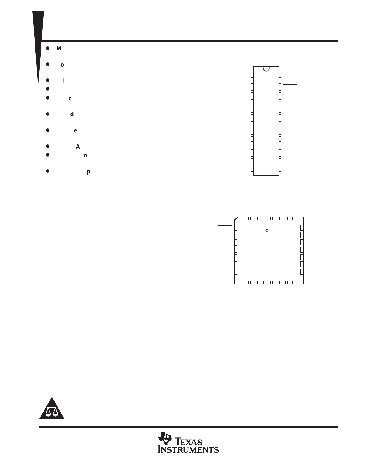
SN54ACT8997 ...JT PACKAGE
SN74ACT8997 . . . DW OR NT PACKAGE
DTDO1
DTDO2
DTDO3
DTDO4
DTMS1
DTMS2
DTMS3
DTMS4
DTCK
DCO
MCO
GND
TDO
TMS
(TOP VIEW)
1
28
2
27
3
26
4
25
5
24
6
23
7
22
8
21
9
20
10
19
11
18
12
17
13
16
14
15
DCI
MCI
TRST
ID1
ID2
ID3
ID4
V
CC
DTDI1
DTDI2
DTDI3
DTDI4
TDI
TCK
Small-Outline (DW) Packages, Ceramic
Chip Carriers (FK), and Standard Plastic
(NT) and Ceramic (JT) 300-mil DIPs
description
The ’ACT8997 are members of the Texas
Instruments SCOPE testability integrated-
circuit family . This family of components facilitates
testing of complex circuit-board assemblies.
The ’ACT8997 enhance the scan capability of TI’s
SCOPE family by allowing augmentation of a
system’s primary scan path with secondary scan
paths (SSPs), which can be individually selected
by the ’ACT8997 for inclusion in the primary scan
SN54ACT8997 . . . FK PACKAGE
TRST
MCI
DCI
DCO
MCO
DTDO1
DTDO2
5
6
7
8
9
10
11
ID1
4
12
(TOP VIEW)
ID2
ID3
321
15 16 17 18
13 14
CC
ID4
V
28 27 26
DTDI1
DTDI2
25
24
23
22
21
20
19
path. These devices also provide buffering of test
signals to reduce the need for external logic.
By loading the proper values into the instruction
DTDO4
DTDO3
GND
DTMS1
DTMS2
DTMS3
DTMS4
register and data registers, the user can select up
to four SSPs to be included in a primary scan path. Any combination of the SSPs can be selected at a time. Any
of the device’s six data registers or the instruction register can be placed in the device’s scan path, i.e., placed
between test data input (TDI) and test data output (TDO) for subsequent shift and scan operations.
DTDI3
DTDI4
TDI
TCK
TMS
TDO
DTCK
All operations of the device except counting are synchronous to the test clock pin (TCK). The 8-bit
programmable up/down counter can be used to count transitions on the device condition input (DCI) pin and
output interrupt signals via the device condition output (DCO) pin. The device can be configured to count on
either the rising or falling edge of DCI.
The test access port (TAP) controller is a finite-state machine compatible with IEEE Standard 1149.1.
The SN54ACT8997 is characterized for operation over the full military temperature range of –55°C to 125°C.
The SN74ACT8997 is characterized for operation from 0°C to 70°C.
Please be aware that an important notice concerning availability, standard warranty, and use in critical applications of
Texas Instruments semiconductor products and disclaimers thereto appears at the end of this data sheet.
SCOPE and EPIC are trademarks of Texas Instruments Incorporated.
PRODUCTION DATA information is current as of publication date.
Products conform to specifications per the terms of Texas Instruments
standard warranty. Production processing does not necessarily include
testing of all parameters.
POST OFFICE BOX 655303 • DALLAS, TEXAS 75265
Copyright 1996, Texas Instruments Incorporated
On products compliant to MIL-PRF-38535, all parameters are tested
unless otherwise noted. On all other products, production
processing does not necessarily include testing of all parameters.
1
SN54ACT8997, SN74ACT8997
SCAN-PATH LINKERS WITH 4-BIT IDENTIFICATION BUSES
SCAN-CONTROLLED IEEE STD 1149.1 (JTAG) TAP CONCATENATORS
SCAS157D – APRIL 1990 – REVISED DECEMBER 1996
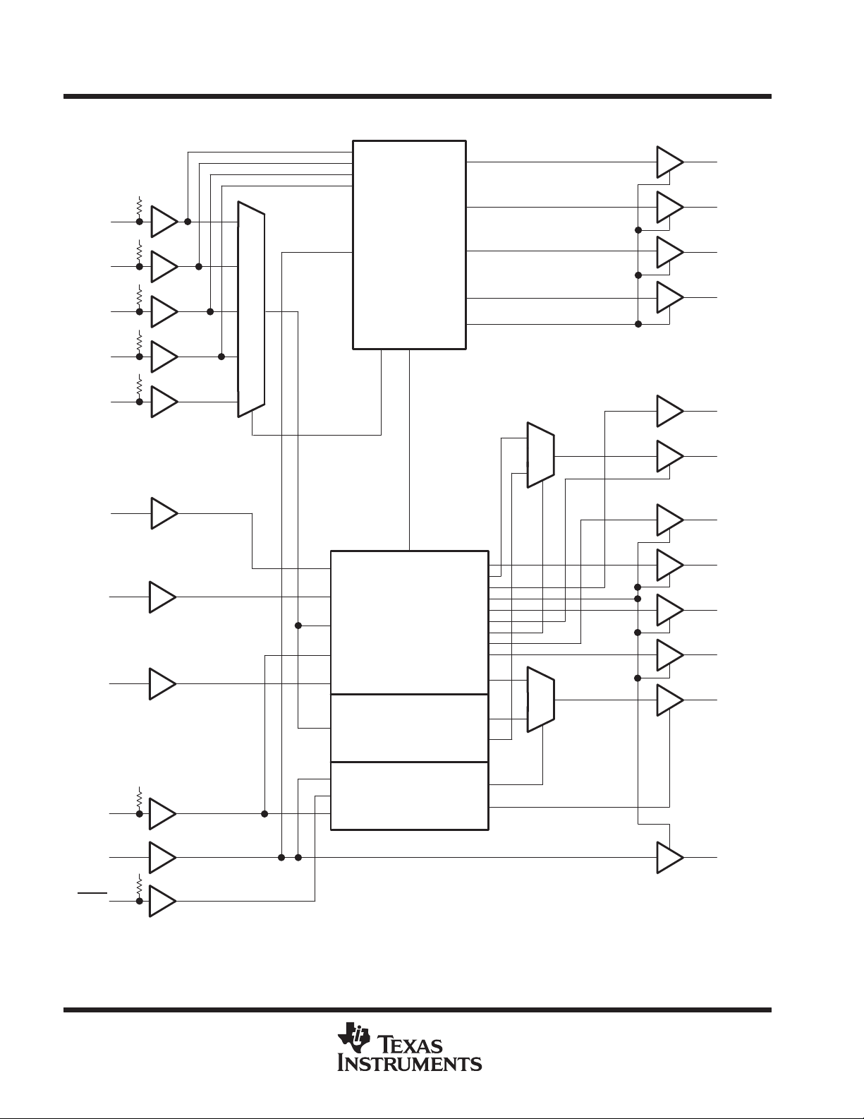
functional block diagram
3
DTDO1
TDI
DTDI1
DTDI2
DTDI3
DTDI4
DCI
MCI
ID(1–4)
V
CC
16
V
CC
20
V
CC
19
V
CC
18
V
CC
17
28
27
22–25
Scan-Path
Configuration
Data
Registers
Instruction
Register
4
DTDO2
5
DTDO3
6
DTDO4
2
MCO
1
DCO
(3 state or
open drain)
8
DTMS1
9
DTMS2
10
DTMS3
11
DTMS4
13
TDO
V
CC
14
TMS
15
TCK
V
CC
26
TRST
Pin numbers shown are for the DW, JT, and NT packages.
2
POST OFFICE BOX 655303 • DALLAS, TEXAS 75265
Test Port
12
DTCK

SN54ACT8997, SN74ACT8997
SCAN-PATH LINKERS WITH 4-BIT IDENTIFICATION BUSES
SCAN-CONTROLLED IEEE STD 1149.1 (JTAG) TAP CONCATENATORS
SCAS157D – APRIL 1990 – REVISED DECEMBER 1996
functional block description
The ’ACT8997 is intended to link secondary scan paths for inclusion in a primary scan path. Any combination
of the four secondary scan paths can be linked, or the device can be bypassed entirely.
The least-significant bit (LSB) of any value scanned into any register of the device is the first bit shifted in
(nearest to TDO). The most-significant bit (MSB) is the last bit shifted in (nearest to TDI).
The ’ACT8997 is divided into functional blocks as detailed below.
test port
The test port decodes the signals on TCK, TMS, and TRST to control the operation of the circuit. The test port
includes a TAP controller that issues the proper control instructions to the data registers according to the
IEEE Standard 1149.1 protocol. The T AP controller state diagram is shown in Figure 1.
instruction register
The instruction register (IR) is an 8-bit-wide serial-shift register that issues commands to the device. Data is
input to the instruction register via TDI (or one of the DTDI pins) and shifted out via TDO. All device operations
are initiated by loading the proper instruction or sequence of instructions into the IR.
data registers
Six parallel data registers are included in the ’ACT8997: bypass, control, counter, boundary-scan, ID-bus, and
select. The ID bus register is a part of the boundary-scan register. Each data register is serially loaded via TDI
or DTDI and outputs data via TDO. Table 1 summarizes the registers in the ’ACT8997.
scan-path-configuration circuit
This circuit decodes bits in the select and control registers to determine which, if any, of the secondary scan
paths are to be included in the primary scan path.
T able 1. Register Summary
REGISTER
NAME
Instruction 8 Issue command information to the device
Control 10 Configuration and enable control
Counter 8 Count events on DCI, output interrupts via DCO
Select 8 Select one or more secondary scan paths
Boundary Scan 10 Capture and force test data at device periphery
ID Bus 4 Provide subsystem identification code
Bypass 1 Remove the ’ACT8997 from the scan path
LENGTH
(BITS)
FUNCTION
POST OFFICE BOX 655303 • DALLAS, TEXAS 75265
3

SN54ACT8997, SN74ACT8997
SCAN-PATH LINKERS WITH 4-BIT IDENTIFICATION BUSES
SCAN-CONTROLLED IEEE STD 1149.1 (JTAG) TAP CONCATENATORS
SCAS157D – APRIL 1990 – REVISED DECEMBER 1996
Terminal Functions
TERMINAL
NAME
DCI I
DCO O
DTCK O Device test clock. DTCK outputs the buffered test clock TCK to the secondary scan path(s).
DTDI1
DTDI2
DTDI3
DTDI4
DTDO1
DTDO2
DTDO3
DTDO4
DTMS1
DTMS2
DTMS3
DTMS4
GND Ground
IDI
ID2
ID3
ID4
MCI I
MCO O Master condition output. MCO transmits interrupt and protocol signals to the secondary scan path(s).
TCK I
TDI I
TDO O
TMS I
TRST
V
CC
I/O DESCRIPTION
Device condition input. DCI receives interrupt and protocol signals from the secondary scan path(s). When the
counter register is instructed to count up or down, DCI is configured as the counter clock.
Device condition output. DCO is configured by the control register to output protocol and interrupt signals and can
be configured by the control register to output an error signal if the instruction register is loaded with an invalid value.
DCO is further configured by the control register as:
Active high or active low (reset condition = active low)
Open drain or 3 state (reset condition = open drain)
Device test data input 1–4. DTDI1–DTDI4 receive the serial test data output(s) of the selected secondary scan
I
path(s). An internal pullup forces DTDI1–DTDI4 to a high logic level if it is left unconnected.
O Device test data output 1–4. These outputs send serial test data to the TDI input(s) of the secondary scan path(s).
Device test mode select 1–4. Any combination of these four outputs can be selected to follow TMS to direct the
secondary scan path(s) through the TAP controller states in Figure 1. The unselected DTMS outputs can be set
O
independently to a high or low logic level. The TMS circuit monitors input from the select register to determine the
configuration of the DTMS outputs.
Identification 1–4. This 4-bit data bus can be hardwired to provide identification of the subsystem under test. The
I
value present on the bus can be scanned out through the boundary scan or ID bus registers.
Master condition input. MCI receives interrupt and protocol signals from a primary bus controller (PBC). The level
on MCI is buffered and output on MCO.
Test clock. One of four terminals required by IEEE Standard 1149.1. All operations of the ’ACT8997 except for the
count function are synchronous to TCK. Data on the device inputs is captured on the rising edge of TCK, and outputs
change on the falling edge of TCK.
T est data input. One of four terminals required by IEEE Standard 1149.1. TDI is the serial input for shifting information
into the instruction register or selected data register . TDI is typically driven by the TDO of the PBC. An internal pullup
forces TDI to a high level if left unconnected.
Test data output. One of four terminals required by IEEE Standard 1149.1. TDO is the serial output for shifting
information out of the instruction register or selected data register . TDO is typically connected to the TDI of the next
scannable device in the primary scan path.
Test mode select. One of four terminals required by IEEE Standard 1149.1. The level of TMS at the rising edge of
TCK directs the ’ACT8997 through its TAP controller states. An internal pullup forces TMS to a high level if left
unconnected.
Test reset. This active-low input implements the optional reset terminal of IEEE Standard 1149.1. When asserted,
TRST
I
causes the ’ACT8997 to go to the Test-Logic-Reset state and configure the instruction register and data
registers to their power-up values. An internal pullup forces TRST
Supply voltage
to a high level if left unconnected.
4
POST OFFICE BOX 655303 • DALLAS, TEXAS 75265
SN54ACT8997, SN74ACT8997
SCAN-PATH LINKERS WITH 4-BIT IDENTIFICATION BUSES
SCAN-CONTROLLED IEEE STD 1149.1 (JTAG) TAP CONCATENATORS
SCAS157D – APRIL 1990 – REVISED DECEMBER 1996
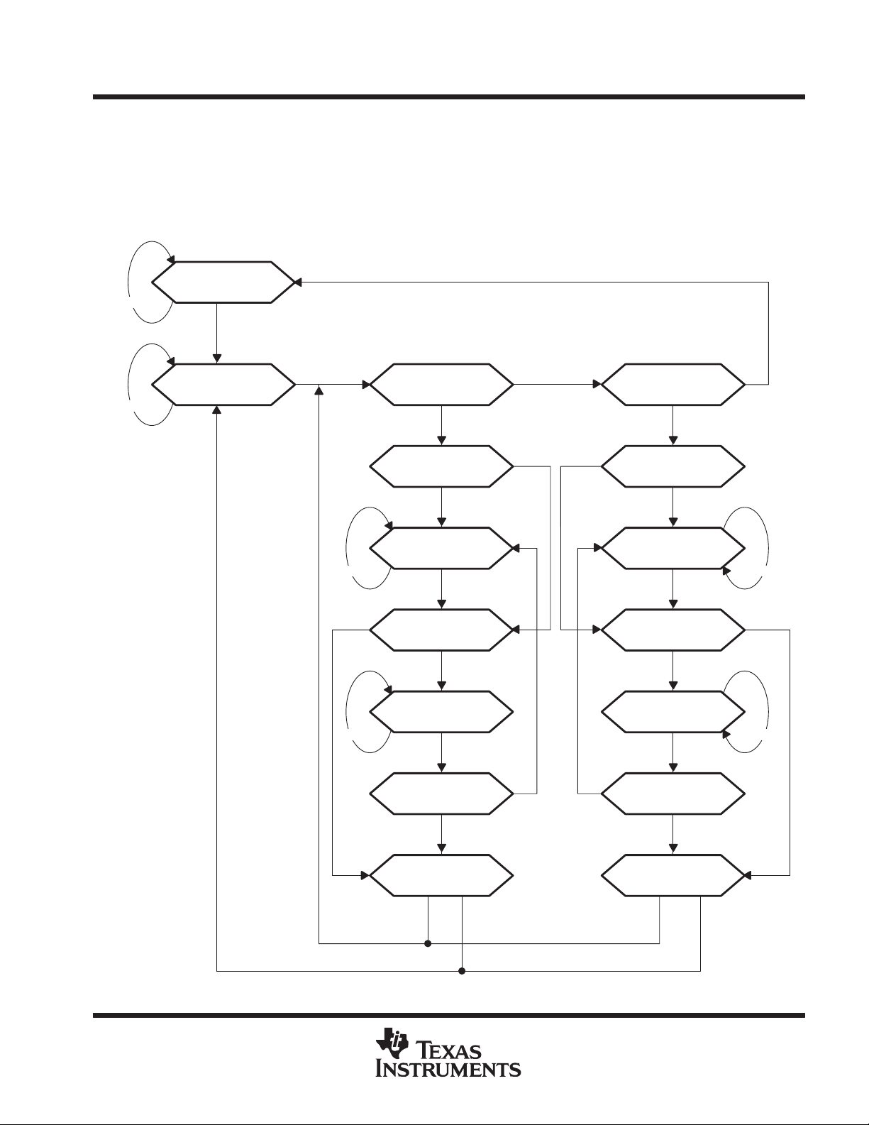
state diagram description
The T AP proceeds through the states in Figure 1 according to IEEE Standard 1149.1. There are six stable states
(indicated by a looping arrow) and ten unstable states in the diagram. A stable state is a state the T AP can retain
for consecutive TCK cycles. Any state that does not meet this criterion is an unstable state.
There are two main paths through the state diagram: one to manipulate a data register and one to manipulate
the instruction register. No more than one register can be manipulated at a time.
Test-Logic-Reset
TMS = H
TMS = L
TMS = L
Run-Test/Idle
TMS = H
TMS = H
Select-DR-Scan Select-IR-Scan
TMS = L
Capture-DR
TMS = L
Shift-DR
TMS = L TMS = L
TMS = H TMS = H
TMS = H
Exit1-DR
TMS = L TMS = L
Pause-DR
TMS = L
TMS = H
TMS = H
TMS = L
TMS = H TMS = H
Capture-IR
TMS = L
Shift-IR
Exit1-IR
Pause-IR
TMS = H
TMS = L TMS = L
TMS = H
TMS = L
Exit2-DR
TMS = H
Update-DR
TMS = H TMS = H
TMS = L TMS = L
Figure 1. TAP-Controller State Diagram
POST OFFICE BOX 655303 • DALLAS, TEXAS 75265
Exit2-IR
TMS = H
Update-IR
5

SN54ACT8997, SN74ACT8997
SCAN-PATH LINKERS WITH 4-BIT IDENTIFICATION BUSES
SCAN-CONTROLLED IEEE STD 1149.1 (JTAG) TAP CONCATENATORS
SCAS157D – APRIL 1990 – REVISED DECEMBER 1996
Test-Logic-Reset
In this state, the test logic is inactive and an internal reset signal is applied to all registers in the device. During
device operation, the TAP returns to this state in no more than five TCK cycles if the test mode select (TMS)
input is high. The TMS pin has an internal pullup that forces it to a high level if it is left unconnected or if a board
defect causes it to be open circuited. The device powers up in the Test-Logic-Reset state.
Run-Test/Idle
The TAP must pass through this state before executing any test operations. The TAP may retain this state
indefinitely , and no registers are modified while in Run-T est/Idle. The 8-bit programmable up/down counter can
be operated in this state.
Select-DR-Scan, Select-IR-Scan
No specific function is performed in these states; the TAP exits either of them on the next TCK cycle.
Capture-DR
The selected data register is placed in the scan path (i.e., between TDI and TDO). Depending on the current
instruction, data may or may not be loaded or captured by that register on the rising edge of TCK, causing the
TAP state to change.
Shift-DR
In this state, data is serially shifted through the selected data register from TDI to TDO on each TCK cycle. The
first shift does not occur until the first TCK cycle after entering this state (i.e., no shifting occurs during the TCK
cycle in which the T AP changes from Capture-DR to Shift-DR or from Exit2-DR to Shift-DR). On the falling edge
of TCK in Shift-DR, TDO goes from the high-impedance state to the active state. TDO enables to the value
present in the least-significant bit of the selected data register.
Exit1-DR, Exit2-DR
These are temporary states that end the shifting process. It is possible to return to the Shift-DR state from either
Exit1-DR or Exit2-DR without recapturing the data register. The last shift occurs on the TCK cycle in which the
T AP state changes from Shift-DR to Exit-DR. TDO changes from the active state to the high-impedance state
on the falling edge of TCK in Exit1-DR.
Pause-DR
The TAP can remain in this state indefinitely. The Pause-DR state suspends and resumes shift operations
without loss of data.
Update-DR
If the current instruction calls for the latches in the selected data register to be updated with current data, the
latches are updated only during this state.
Capture-IR
The instruction register is preloaded with the IR status word (see Table 4) and placed in the scan path.
Shift-IR
In this state, data is serially shifted through the instruction register from TDI to TDO on each TCK cycle. The
first shift does not occur until the first TCK cycle after entering this state (i.e., no shifting occurs during the TCK
cycle in which the T AP changes from Capture-IR to Shift-IR or from Exit2-IR to Shift-IR). On the falling edge of
TCK in Shift-IR, TDO goes from the high-impedance state to the active state, and will enable to a high level.
6
POST OFFICE BOX 655303 • DALLAS, TEXAS 75265
SN54ACT8997, SN74ACT8997
SCAN-PATH LINKERS WITH 4-BIT IDENTIFICATION BUSES
SCAN-CONTROLLED IEEE STD 1149.1 (JTAG) TAP CONCATENATORS
SCAS157D – APRIL 1990 – REVISED DECEMBER 1996
Exit1-IR, Exit2-IR
These are temporary states that end the shifting process. It is possible to return to the Shift-IR state from either
Exit1-IR or Exit2-IR without recapturing the instruction register. The last shift occurs on the TCK cycle in which
the T AP state changes from Shift-IR to Exit1-IR. TDO changes from the active state to the high-impedance state
on the falling edge of TCK in Exit1-IR.
Pause-IR
The T AP can remain in this state indefinitely. The Pause-IR state suspends and resumes shift operations without
loss of data.
Update-IR
In this state, the latches shadowing the instruction register are updated with the new instruction.
instruction-register description
The instruction register (IR) is an 8-bit serial register that outputs control signals to the device. Table 2 lists the
instructions implemented in the ’ACT8997 and the data register selected by each instruction. The MSB of the
IR is an even-parity bit. If the value scanned into the IR during Shift-IR does not contain even parity, an error
signal (IRERR
via DCO if the TAP enters the Pause-IR state.
) is generated internally as shown in T able 3. The ’ACT8997 can be configured to output IRERR
During the Capture-IR state, the IR status word is loaded.The IR status word contains information about the
most recently loaded value of the instruction register and the logic level present at the DCI input. The IR status
word is encoded as shown in Table 4. Figure 2 shows the order of scan for the IR.
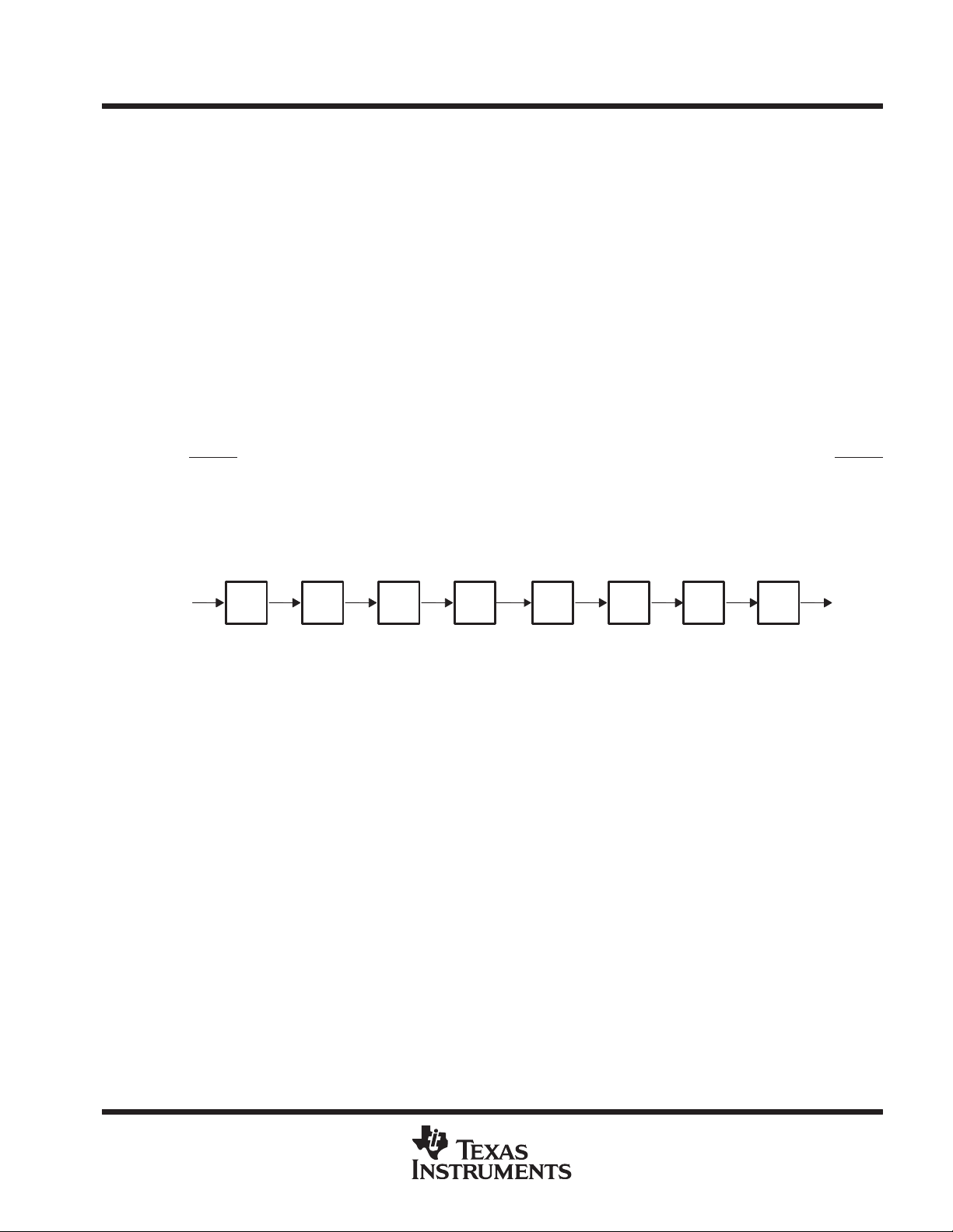
TDI or DTDI
Bit 7
(MSB)
Bit 6 Bit 5 Bit 4 Bit 3 Bit 2 Bit 1
Bit 0
(LSB)
Figure 2. Instruction-Register Bits and Order of Scan
TDO
POST OFFICE BOX 655303 • DALLAS, TEXAS 75265
7
SN54ACT8997, SN74ACT8997
SCAN-PATH LINKERS WITH 4-BIT IDENTIFICATION BUSES
SCAN-CONTROLLED IEEE STD 1149.1 (JTAG) TAP CONCATENATORS
SCAS157D – APRIL 1990 – REVISED DECEMBER 1996
Table 2. Instruction-Register Opcodes
BINARY CODE
BIT 7 → BIT 0
MSB → LSB
00000000 00 EXTEST Boundary scan Boundary scan Test
10000001 81 BYPASS
10000010 82 SAMPLE/PRELOAD Sample boundary Boundary scan Normal
0000001 1 03 INTEST Boundary scan Boundary scan Test
10000100 84 BYPASS
00000101 05 BYPASS
00000110 06 BYPASS
10000111 87 BYPASS
10001000 88 COUNT Count Bypass Normal
00001001 09 COUNT Count Bypass Normal
00001010 0A BYPASS
10001011 8B BYPASS
00001100 0C BYPASS
10001101 8D BYPASS Bypass scan Bypass Normal
10001110 8E SCANCN Control register scan Control Normal
00001 111 0F SCANCN Control register scan Control Normal
11111010 FA SCANCNT Counter scan Counter Normal
01111011 7B READCNT Counter read Counter Normal
11111100 FC SCANIDB ID bus register scan ID bus Normal
01111101 7D READIDB ID bus register read ID bus Normal
01111110 7E SCANSEL Select register scan Select Normal
All others BYPASS Bypass scan Bypass Normal
†
A SCOPE opcode exists but is not supported by the ’ACT8997.
HEX
VALUE
SCOPE OPCODE DESCRIPTION
SELECTED DATA
REGISTER
†
†
†
†
†
†
†
†
Bypass scan Bypass Normal
Bypass scan Bypass Normal
Bypass scan Bypass Normal
Bypass scan Bypass Normal
Bypass scan Bypass Normal
Bypass scan Bypass Normal
Bypass scan Bypass Normal
Bypass scan Bypass Normal
MODE
Table 3. IRERR Function Table
NO. OF INSTRUCTION
REGISTER BITS = 1
0, 2, 4, 6, 8 1
1, 3, 5, 7 0
IRERR
Table 4. Instruction-Register Status Word
IR BIT VALUE
7 IRERR (see Table 3)
6 0
5 0
4 0
3 DCI (1 = active, 0 = inactive)
2 0
1 0
0 1
†
This value is loaded in the instruction
register during the Capture-IR TAP state.
†
8
POST OFFICE BOX 655303 • DALLAS, TEXAS 75265

SN54ACT8997, SN74ACT8997
SCAN-PATH LINKERS WITH 4-BIT IDENTIFICATION BUSES
SCAN-CONTROLLED IEEE STD 1149.1 (JTAG) TAP CONCATENATORS
SCAS157D – APRIL 1990 – REVISED DECEMBER 1996
instruction-register opcode description
The operation of the ’ACT8997 is dependent on the instruction loaded into the IR. Each instruction selects one
of the data registers to be placed between TDI or DTDI and TDO during the Shift-DR T AP state. All the required
instructions of IEEE Standard 1149.1 are implemented in the ’ACT8997.
boundary scan
This instruction implements the required EXTEST and optional INTEST operations of IEEE Standard 1 149.1.
The boundary-scan register (which includes the ID-bus register) is placed in the scan path. Data appearing at
input pins included in the boundary-scan register is captured. Data previously loaded into the output pins
included in the boundary-scan register is forced through the outputs.
bypass scan
This instruction implements the required BYP ASS operation of IEEE Standard 1149.1. The bypass register is
placed in the scan path and preloads with a logic 0 during Capture-DR.
sample boundary
This instruction implements the required SAMPLE/PRELOAD operation of IEEE Standard 1149.1. The
boundary-scan register is placed in the scan path, and data appearing at the inputs and outputs included in the
boundary-scan register is sampled on the rising edge of TCK in Capture-DR.
count
The counter register begins counting on each DCI transition. The count begins from the value present in the
register before the count instruction was loaded. The counter can be configured by the control register to count
up or down on either the low-to-high or high-to-low transition of DCI. Counting occurs only while in the
Run-Test/Idle TAP state.
control-register scan
The control register is placed in the scan path for a subsequent shift operation. The register is not preloaded
during Capture-DR.
counter-register scan
The counter register is placed in the scan path. During Capture-DR, the current value of the counter is loaded
in the counter register. At Update-DR, the newly shifted value is preloaded to the counter.
counter-register read
The counter register is placed in the scan path. During Capture-DR, the prior preload value of the counter is
loaded into the counter register. At Update-DR, the newly shifted value is preloaded to the counter.
ID-bus-register scan
The ID-bus register (a subset of the boundary-scan register) is placed in the scan path for a subsequent shift
operation. The data appearing on the ID bus is loaded into the ID-bus register on the rising edge of TCK in
Capture-DR.
ID-bus-register read
The ID-bus register is placed in the scan path for a subsequent shift operation. The register is not preloaded
during Capture-DR.
select-register scan
The select register is placed in the scan path for a subsequent shift operation. The register is not preloaded
during Capture-DR.
POST OFFICE BOX 655303 • DALLAS, TEXAS 75265
9

SN54ACT8997, SN74ACT8997
9
8
7
6, 5
4
3
2
1
0
SCAN-PATH LINKERS WITH 4-BIT IDENTIFICATION BUSES
SCAN-CONTROLLED IEEE STD 1149.1 (JTAG) TAP CONCATENATORS
SCAS157D – APRIL 1990 – REVISED DECEMBER 1996
control register description
The control register (CTLR) is a 10-bit serial register that controls the enable and select functions of the
’ACT8997. A reset operation forces all bits to a low logic level. The contents of the CTLR are latched and
decoded during the Update-DR T AP state. The specific function of each bit is listed in Table 5. The enable and
select functions of the CTLR bits are mapped as follows:
Table 5. Control-Register Bit Mapping
BIT VALUE FUNCTION
0 Configure counter to count up
1 Configure counter to count down
0 Do not stop counting when the count reaches 00000000
1 Stop counting when the count reaches 00000000 (count down only)
0 Configure DCO as an active-low output
1 Configure DCO as an active-high output
00 DCO = Inactive (level depends on CTLR bit 7)
01
DCO = IRERR
10
DCO = CE, an internal logic 0 generated when the count is 00000000 (count down) or 11111111 (count up)
11 DCO = DCI
0
Do not mask IRERR from DCO
1
Mask IRERR from DCO
0 Configure DCO as an open-drain output
1 Configure DCO as a 3-state output
0 Disable DCO
1 Enable DCO
0 Configure DCI as an active-low input
1
Configure DCI as an active-high input
0 Enable DTCK, DTDO(1–4), and DTMS(1–4) [outputs DTDO(1–4) depend on select register (see Table 7)]
1 Disable DTCK, DTDO(1–4), and DTMS(1–4)
Bit 9–Up/Down
This bit sets the count mode of the counter register (reset condition = count up).
Bit 8 – Latch on Zero
The counter register can be configured to stop counting when its value is 00000000 and ignore subsequent
transitions on the counter clock, DCI. The latch-on-zero option is valid only in the count-down mode
(reset condition = do not latch on zero). The value of this bit has no effect on the operation of the counter if
CTLR bit 9 = 0.
Bit 7 – DCO Polarity Select
DCO can be configured as an active-low or active-high output (reset condition = active low).
Bit 6/Bit 5 – DCO Source Select 1/DCO Source Select 0
DCO can be used to output the IRERR
signal generated by the ’ACT8997 (see Table 3). Bits 6 and 5 can be
set to output IRERR via DCO on the falling edge of TCK in the Pause-IR state. DCO can also be configured
to become active when the value of the counter is 00000000, to follow DCI, or be set to a static high or low level
(reset condition = static high level).
10
POST OFFICE BOX 655303 • DALLAS, TEXAS 75265

SN54ACT8997, SN74ACT8997
SCAN-PATH LINKERS WITH 4-BIT IDENTIFICATION BUSES
SCAN-CONTROLLED IEEE STD 1149.1 (JTAG) TAP CONCATENATORS
SCAS157D – APRIL 1990 – REVISED DECEMBER 1996
Bit 4 – Parity Mask
The signal IRERR can be masked from appearing on DCO even if bits 6 and 5 are set such that it is output in
the Pause-IR state (reset condition = do not mask IRERR
Bit – DCO Drive Select
DCO can be configured as either an open-drain or 3-state output (reset condition = open drain). The open-drain
configuration allows multiple DCO outputs to be used in a wired-OR or wired-AND application. The 3-state
configuration allows the DCO output to be connected to a bus.
Bit 2 – DCO Enable
When configured as a 3-state output, DCO can be placed in the high-impedance state
(reset condition = disabled). If configured as an open-drain output and disabled, DCO outputs a high level.
Bit 1 – DCI Polarity Select
DCI can be configured as an active-low or active-high input (reset condition = active low).
Bit 0 – Device Test Pins Output Enable (active low)
DTCK, DTDO1–4, and DTMS1–4 pins can be placed in the high-impedance state (disabled) with this bit
(reset condition = not disabled). If DTDO1–4 pins are not disabled using this control bit, then their drive state
is dependent on the value of the select register (see Table 7).
).
Several CTLR bits affect the functionality of the DCO output. The DCO function table is given in T able 6. Figure 3
illustrates the order of scan for the CTLR.
TDI or DTDI
Bit 9
(MSB)
Bit 8 Bit 7 Bit 6 Bit 5 Bit 4 Bit 3 Bit 2 Bit 1
Bit 0
(LSB)
Figure 3. Control-Register Bits and Order of Scan
TDO
POST OFFICE BOX 655303 • DALLAS, TEXAS 75265
11

SN54ACT8997, SN74ACT8997
SCAN-PATH LINKERS WITH 4-BIT IDENTIFICATION BUSES
SCAN-CONTROLLED IEEE STD 1149.1 (JTAG) TAP CONCATENATORS
SCAS157D – APRIL 1990 – REVISED DECEMBER 1996
Table 6. DCO Function Table
INTERNAL
DCI
X X X X X X X 0 0 X H
X X X X X X X 1 0 X Z
X X X 0 0 0 X X 1 X H
X X X 1 0 0 X X 1 X L
X X X 0 0 1 1 X 1 X H
X X X 1 0 1 1 X 1 X L
X 0 X 0 0 1 0 X 1 X L in Pause-IR§, H otherwise
X 1 X 0 0 1 0 X 1 X H
X 0 X 1 0 1 0 X 1 X H in Pause-IR§, L otherwise
X 1 X 1 0 1 0 X 1 X L
X X 0 0 1 0 X X 1 X L
X X 0 1 1 0 X X 1 X H
X X 1 0 1 0 X X 1 X H
X X 1 1 1 0 X X 1 X L
L X X 1 1 1 X X 1 0 H
L X X 1 1 1 X X 1 1 L
L X X 0 1 1 X X 1 0 L
L X X 0 1 1 X X 1 1 H
H X X 1 1 1 X X 1 0 L
H X X 1 1 1 X X 1 1 H
H X X 0 1 1 X X 1 0 H
H X X 0 1 1 X X 1 1 L
†
These signals are generated as described elsewhere in this data sheet.
‡
The control register must contain these values after the TAP has passed through its most recent Update-DR state.
§
DCO becomes active on the falling edge of TCK as the TAP enters the Pause-IR state and becomes inactive on the
falling edge of TCK as the T AP enters Exit2-IR.
SIGNALS
IRERR
†
CE BIT 7 BIT 6 BIT 5 BIT 4 BIT 3 BIT 2 BIT 1
CONTROL-REGISTER BITS
‡
DCO
12
POST OFFICE BOX 655303 • DALLAS, TEXAS 75265

SN54ACT8997, SN74ACT8997
SCAN-PATH LINKERS WITH 4-BIT IDENTIFICATION BUSES
SCAN-CONTROLLED IEEE STD 1149.1 (JTAG) TAP CONCATENATORS
SCAS157D – APRIL 1990 – REVISED DECEMBER 1996
select register description
The select register (SR) is an 8-bit serial register that determines which, if any, of the secondary scan paths
(SSPs) will be included in the primary scan path. A reset operation forces all bits to a logic 0. The register is
divided into four 2-bit sections, each of which controls one SSP. Figure 4 shows the mapping of the bits to the
SSPs and the order of scan. For each SSP, the higher-order bit is the MSB and the lower-order bit is the LSB
(e.g., bit 3 is the MSB of SSP2 and bit 2 is the LSB of SSP2).
TDI or DTDI
Bit 7
(MSB)
Bit 6 Bit 5 Bit 4 Bit 3 Bit 2 Bit 1
SSP4 SSP3 SSP2 SSP1
Bit 0
(LSB)
Figure 4. Select Register Bits and Order of Scan
When a new 8-bit value is loaded into the SR, the configuration of one or more DTMS pins may change. If the
new value of the SR configures a DTMS pin to a static (high or low) level, it assumes that level on the falling
edge of TCK in the Update-DR T AP state. This condition is independent of any previous SR configurations. If
the new value of the SR forces a DTMS pin to follow TMS (i.e., select the secondary scan path) and one or more
DTMS pins are currently in the TMS-follow mode, the transfer of DTMS lines occurs on the falling edge of TCK
in the Update-DR T AP state. If, however, the new configuration forces a DTMS pin to follow TMS while no other
DTMS pin is selected, the DTMS pin is forced low and does not begin following TMS until the falling edge of
TCK in the Run-T est/Idle TAP state; therefore, when an SSP is initially selected, the T AP state should travel from
Update-DR to Run-Test/Idle, not from Update-DR to Select-DR-Scan.
Although any combination of SSPs can be selected, the order of scan for each combination is fixed (see data
flow description for details). The SR bit decoding is shown in Table 7.
Table 7. Select Register-Bit Decoding
MSB LSB
0 0 H Z
0 1 L Z
1 X TMS Active
†
The DTDO1–4 outputs are active only in
the Shift-IR and Shift-DR TAP states.
DTMS
SOURCE
DTDO
STATUS
†
TDO
POST OFFICE BOX 655303 • DALLAS, TEXAS 75265
13

SN54ACT8997, SN74ACT8997
SCAN-PATH LINKERS WITH 4-BIT IDENTIFICATION BUSES
SCAN-CONTROLLED IEEE STD 1149.1 (JTAG) TAP CONCATENATORS
SCAS157D – APRIL 1990 – REVISED DECEMBER 1996
boundary-scan register/ID-bus register description
The boundary-scan register (BSR) is a 10-bit serial register that can be used to capture data appearing at
selected device inputs, force data through device outputs, and apply data to the device’s internal logic. The BSR
is made up of boundary-scan cells (BSCs). T able 8 lists the device signal for each of the 10 BSCs that comprise
the BSR. A reset operation does not affect the contents of the BSR.
Table 8. Boundary-Scan Register Bit Mapping
BIT
†
This internal signal cannot be observed from the I/O terminals of the device.
TERMINAL
NAME
9 MCI Master condition in
8 MCO Master condition out
7 DCI Device condition in
6 DCOTS
5 DCOOD
4 DCO Device condition out
3 ID4 Identification bus bit 4
2 ID3 Identification bus bit 3
1 ID2 Identification bus bit 2
0 ID1 Identification bus bit 1
†
Enable control for DCO in 3-state configuration (active low)
†
Enable control for DCO in open-drain configuration (active low)
SIGNAL DESCRIPTION
The four BSCs connected to the ID(1–4) terminals form a subset of the BSR called the ID-bus register (IDBR).
The IDBR can be scanned without accessing the remaining BSCs of the BSR. Figure 5 shows the order of scan
for the BSR and IDBR.
TDI or DTDI
TDI or DTDI
Bit 9
(MSB)
Bit 8 Bit 7 Bit 6 Bit 5 Bit 4 Bit 3 Bit 2 Bit 1
IDBR
Bit 0
(LSB)
TDO
BSR
Figure 5. Boundary-Scan Register Bits and Order of Scan
bypass register description
The bypass register (BR) is a 1-bit serial register. The BR provides a means of effectively removing the
’ACT8997 from the primary scan path when it is not needed for the current test operation. Any selected
secondary scan paths remain active in the primary scan path as described in the data flow description. At power
up, the BR is placed in the scan path. During Capture-DR, the BR is preloaded with a low logic level. Figure 6
shows the order of scan for the bypass register.
Bit 0
Figure 6. Bypass-Register Bit and Order of Scan
TDOTDI or DTDI
14
POST OFFICE BOX 655303 • DALLAS, TEXAS 75265

SN54ACT8997, SN74ACT8997
SCAN-PATH LINKERS WITH 4-BIT IDENTIFICATION BUSES
SCAN-CONTROLLED IEEE STD 1149.1 (JTAG) TAP CONCATENATORS
SCAS157D – APRIL 1990 – REVISED DECEMBER 1996
counter register description
The counter register (CNTR) is an 8-bit serial register and an associated 8-bit parallel-load up/down counter.
A reset operation forces all bits of the shift register to a logic 0 but does not affect the counter . The counter can
be preloaded with an initial value before counting begins, and the current value of the counter scanned out via
the shift register. The CNTR can be used to count events occurring on the secondary scan path(s) using the
DCI pin as a counter clock and can output interrupt signals via DCO when the count has reached its end value.
An internal signal, CE
, is generated as a logic 0 when the count reaches its end value (i.e., 00000000 for count
down, 1 1111111 for count up). For any other count value, CE is a logic 1. Many of the features of the CNTR are
configured by a bit in the CTLR including:
Count direction up or down (control register bit 9; reset condition = count up).
Stop counting upon counting down to 00000000 (control register bit 8; reset condition = do not latch on zero).
Output CE
signals at DCO (control register bits 5 and 6; reset condition = do not output CE at DCO).
Edge of DCI on which to trigger (control register bit 1; reset condition = positive edge).
Figure 7 shows the order of scan for the CNTR.
TDI or DTDI
Bit 7
(MSB)
Bit 6 Bit 5 Bit 4 Bit 3 Bit 2 Bit 1
Bit 0
(LSB)
Figure 7. Counter-Register Bits and Order of Scan
TDO
POST OFFICE BOX 655303 • DALLAS, TEXAS 75265
15

SN54ACT8997, SN74ACT8997
SCAN-PATH LINKERS WITH 4-BIT IDENTIFICATION BUSES
SCAN-CONTROLLED IEEE STD 1149.1 (JTAG) TAP CONCATENATORS
SCAS157D – APRIL 1990 – REVISED DECEMBER 1996
data flow description
The direction of serial-data flow in the ’ACT8997 is dependent on the current instruction and value of the SR.
Figure 8 shows the data flow when one or more SSPs have been selected. When more than one SSP has been
selected, the order of scan is determined by which SSPs have been selected as shown in T able 9. The ’ACT8997
add one bit of delay from TDI or DTDI to DTDO.
’ACT8997
TDI TDO
NO SECONDARY SCAN PATH SELECTED
IR or
Selected DR
’ACT8997
TDI DTDOn TDI TDO DTDIn TDO(1-bit delay) SSPn
ONE SECONDARY SCAN PATH SELECTED
’ACT8997
TDI DTDOx TDI TDO
(1-bit delay) SSPx
’ACT8997
DTDIx DTDOn(1-bit delay) TDI TDOSSPn
’ACT8997
DTDIn DTDOm(1-bit delay) TDI TDOSSPm
MULTIPLE SECONDARY SCAN PATHS SELECTED
Selected Scan Path
Selected Scan Path
Selected Scan Path
Selected Scan Path
’ACT8997
IR or
Selected DR
’ACT8997
DTDIm TDO
IR or
Selected DR
16
Figure 8. Data Flow in the ’ACT8997
POST OFFICE BOX 655303 • DALLAS, TEXAS 75265

SCAN-PATH CONFIGURATION
†‡
SN54ACT8997, SN74ACT8997
SCAN-PATH LINKERS WITH 4-BIT IDENTIFICATION BUSES
SCAN-CONTROLLED IEEE STD 1149.1 (JTAG) TAP CONCATENATORS
SCAS157D – APRIL 1990 – REVISED DECEMBER 1996
Table 9. Scan-Path Configurations
SR BIT SSP CONFIGURATION
7 5 3 1 SSP4 SSP3 SSP2 SSP1
0 0 0 0 Inactive Inactive Inactive Inactive TDI–SPL–TDO
0 0 0 1 Inactive Inactive Inactive Active TDI–(1)–SSP1–SPL–TDO
0 0 1 0 Inactive Inactive Active Inactive TDI–(1)–SSP2–SPL–TDO
0 0 1 1 Inactive Inactive Active Active TDI–(1)–SSP1–(1)–SSP2–SPL–TDO
0 1 0 0 Inactive Active Inactive Inactive TDI–(1)–SSP3–SPL–TDO
0 1 0 1 Inactive Active Inactive Active TDI–(1)–SSP1–(1)–SSP3–SPL–TDO
0 1 1 0 Inactive Active Active Inactive TDI–(1)–SSP2–(1)–SSP3–SPL–TDO
0 1 1 1 Inactive Active Active Active TDI–(1)–SSP1–(1)–SSP2–(1)–SSP3–SPL–TDO
1 0 0 0 Active Inactive Inactive Inactive TDI–(1)–SSP4–SPL–TDO
1 0 0 1 Active Inactive Inactive Active TDI–(1)–SSP1–(1)–SSP4–SPL–TDO
1 0 1 0 Active Inactive Active Inactive TDI–(1)–SSP2–(1)–SSP4–SPL–TDO
1 0 1 1 Active Inactive Active Active TDI–(1)–SSP1–(1)–SSP2–(1)–SSP4–SPL–TDO
1 1 0 0 Active Active Inactive Inactive TDI–(1)–SSP3–(1)–SSP4–SPL–TDO
1 1 0 1 Active Active Inactive Active TDI–(1)–SSP1–(1)–SSP3–(1)–SSP4–SPL–TDO
1 1 1 0 Active Active Active Inactive TDI–(1)–SSP2–(1)–SSP3–(1)–SSP4–SPL–TDO
1 1 1 1 Active Active Active Active TDI–(1)–SSP1–(1)–SSP2–(1)–SSP3–(1)–SSP4–SPL–TDO
†
The scan-path configuration is the order of scan, beginning with the TDI of the ’ACT8997 and ending with the TDO of the ’ACT8997.
‡
A (1) indicates one bit of delay through the ’ACT8997. SPL indicates the selected scan register within the ’ACT8997.
absolute maximum ratings over operating free-air temperature range (unless otherwise noted)
Supply voltage range, V
Input voltage range, V
CC
(see Note 1) –0.5 V to VCC + 0.5 V. . . . . . . . . . . . . . . . . . . . . . . . . . . . . . . . . . . . . . . . . . . .
I
Output voltage range, VO (see Note 1) –0.5 V to VCC + 0.5 V. . . . . . . . . . . . . . . . . . . . . . . . . . . . . . . . . . . . . . . . .
Input clamp current, I
Output clamp current, I
Continuous output current, I
Maximum power dissipation at T
(V
< 0 or VI > VCC) ±20 mA. . . . . . . . . . . . . . . . . . . . . . . . . . . . . . . . . . . . . . . . . . . . . . . . .
IK
I
(V
< 0 or VI > VCC) ±20 mA. . . . . . . . . . . . . . . . . . . . . . . . . . . . . . . . . . . . . . . . . . . . . .
OK
I
(V
= 0 to VCC) ±25 mA. . . . . . . . . . . . . . . . . . . . . . . . . . . . . . . . . . . . . . . . . . . . . .
O
O
= 55°C (in still air) (see Note 2): DW package 1.7 W. . . . . . . . . . . . . . . . . .
A
NT package 1.3 W. . . . . . . . . . . . . . . . . . .
Storage temperature range, T
§
Stresses beyond those listed under “absolute maximum ratings” may cause permanent damage to the device. These are stress ratings only, and
functional operation of the device at these or any other conditions beyond those indicated under “recommended operating conditions” is not
implied. Exposure to absolute-maximum-rated conditions for extended periods may affect device reliability.
NOTES: 1. The input and output voltage ratings may be exceeded if the input and output clamp-current ratings are observed.
2. The maximum package power dissipation is calculated using a junction temperature of 150°C and a board trace length of 750 mils,
except for the NT package, which has trace length of zero. For more information, refer to the
application note in the
stg
ABT Advanced BiCMOS Technology Data Book
, literature number SCBD002.
Package Thermal Considerations
–0.5 V to 7 V. . . . . . . . . . . . . . . . . . . . . . . . . . . . . . . . . . . . . . . . . . . . . . . . . . . . . . . . . .
–65°C to 150°C. . . . . . . . . . . . . . . . . . . . . . . . . . . . . . . . . . . . . . . . . . . . . . . . . . . .
§
POST OFFICE BOX 655303 • DALLAS, TEXAS 75265
17

SN54ACT8997, SN74ACT8997
UNIT
IOHHigh-level output current
mA
IOLLow-level output current
mA
SCAN-PATH LINKERS WITH 4-BIT IDENTIFICATION BUSES
SCAN-CONTROLLED IEEE STD 1149.1 (JTAG) TAP CONCATENATORS
SCAS157D – APRIL 1990 – REVISED DECEMBER 1996
recommended operating conditions
SN54ACT8997 SN74ACT8997
MIN MAX MIN MAX
V
V
V
V
V
T
Supply voltage 4.5 5.5 4.5 5.5 V
CC
High-level input voltage 2 2 V
IH
Low-level input voltage 0.8 0.8 V
IL
Input voltage 0 V
I
Output voltage 0 V
O
p
p
Operating free-air temperature –55 125 0 70 °C
A
TDO, DTDO(1–4), MCO –7 –10
DTMS(1–4), DCO (3 state), DTCK –11 –16
TDO, DTDO(1–4), MCO 7 10
DCO (open drain or 3 state) 11 16
DTMS(1–4) 16 24
DTCK 32 48
CC
CC
0 V
0 V
CC
CC
V
V
18
POST OFFICE BOX 655303 • DALLAS, TEXAS 75265

PARAMETER
TEST CONDITIONS
UNIT
TDO, DTDO(1–4), MCO
V
V
V
V
(), ( ),
V
V
TDO, DTDO(1–4), MCO
V
V
DCO (open drain or 3 state)
V
V
V
V
DTMS(1–4)
V
V
DTCK
V
V
,(),
V
5.5 V
SN54ACT8997, SN74ACT8997
SCAN-PATH LINKERS WITH 4-BIT IDENTIFICATION BUSES
SCAN-CONTROLLED IEEE STD 1149.1 (JTAG) TAP CONCATENATORS
SCAS157D – APRIL 1990 – REVISED DECEMBER 1996
electrical characteristics over recommended operating free-air temperature range (unless
otherwise noted)
SN54ACT8997 SN74ACT8997
MIN MAX MIN TYP†MAX
= 4.5
CC
OH
OL
I
OZ
I
OH
I
I
I
CC
∆I
CC
C
i
C
o
C
o
†
Typical values are at VCC = 5 V.
‡
For I/O pins, the parameter IOZ includes the input-leakage current. For the DCO pin, the parameter IOZ includes the open-drain output-leakage
current.
§
This is the increase in supply current for each input being driven at TTL levels rather than VCC or GND.
DTMS(1–4), DCO (3 state),
DTCK
p
DTDO(1–4), DTMS(1–4),
‡
DCO, DTCK
DCO (open drain) VCC = 5.5 V, VO = V
MCI, DCI, TCK, ID(1–4) VCC = 5.5 V, VI = VCC or GND ±1 ±1
TDI, DTDI(1–4),
TMS, TRST
§
DCO VO = VCC or GND 15 pF
All other outputs VO = VCC or GND 10 pF
= 4.5
CC
= 4.5
CC
= 4.5
CC
= 4.5
CC
= 4.5
CC
VCC = 5.5 V, VO = VCC or GND ±10 ±5 µA
=
CC
VCC = 5.5 V, VI = VCC or GND, IO = 0 100 100 µA
VCC = 5.5 V, One input at VI = 3.4 V,
Other inputs at VCC or GND
VI = VCC or GND 6 pF
IOH = –7 mA 3.6
IOH = –10 mA 3.7
IOH = –11 mA 3.6
IOH = –16 mA 3.7
IOL = 7 mA 0.5
IOL = 10 mA 0.5
IOL = 11 mA 0.5
IOL = 16 mA 0.5
IOL = 16 mA 0.5
IOL = 24 mA 0.5
IOL = 32 mA 0.5
IOL = 48 mA 0.5
CC
VI = V
CC
VI = GND –0.1 –20 –0.1 –20
20 10 µA
±1 ±1
1 1 mA
µA
POST OFFICE BOX 655303 • DALLAS, TEXAS 75265
19

SN54ACT8997, SN74ACT8997
UNIT
f
Clock frequenc
MH
tsuSetup time
ns
thHold time
ns
SCAN-PATH LINKERS WITH 4-BIT IDENTIFICATION BUSES
SCAN-CONTROLLED IEEE STD 1149.1 (JTAG) TAP CONCATENATORS
SCAS157D – APRIL 1990 – REVISED DECEMBER 1996
timing requirements over recommended ranges of supply voltage and operating free-air
temperature
SN54ACT8997 SN74ACT8997
MIN MAX MIN MAX
clock
t
w
t
d
* On products compliant to MIL-PRF-38535, this parameter is not production tested.
Pulse duration
p
Delay time Power up to TCK↑ 100* 100 ns
y
TCK 0 20 0 20
DCI (count mode)
TCK high or low 12 12
DCI high or low (count mode)
TRST low 7 7
TMS before TCK↑ 8 8
TDI before TCK↑ 9 9
Any DTDI before TCK↑ 7 7
MCI before TCK↑ 3 3
DCI before TCK↑ 3 2
Any ID before TCK↑ 2 2
TMS after TCK↑ 2 2
TDI after TCK↑ 2 2
Any DTDI after TCK↑ 2 2
MCI after TCK↑ 4 4
DCI after TCK↑ 4 4
Any ID after TCK↑ 4 4
0 20 0 20
7 7
z
ns
20
POST OFFICE BOX 655303 • DALLAS, TEXAS 75265

PARAMETER
UNIT
f
MH
TCK
DTCK
ns
TCK↓
TDO
ns
TCK↓
Any DTDO
ns
TCK↓
Any DTMS
ns
t
TCK↓
ns
t
TCK↓
TMS
Any DTMS
ns
MCI
MCO
ns
t
DCI
ns
t
DCI
TCK↓
TDO
ns
TCK↓
Any DTDO
ns
TCK↓
Any DTMS
ns
TCK↓
DCO
ns
TCK↓
TDO
ns
TCK↓
Any DTDO
ns
TCK↓
Any DTMS
ns
TCK↓
DCO
ns
SN54ACT8997, SN74ACT8997
SCAN-PATH LINKERS WITH 4-BIT IDENTIFICATION BUSES
SCAN-CONTROLLED IEEE STD 1149.1 (JTAG) TAP CONCATENATORS
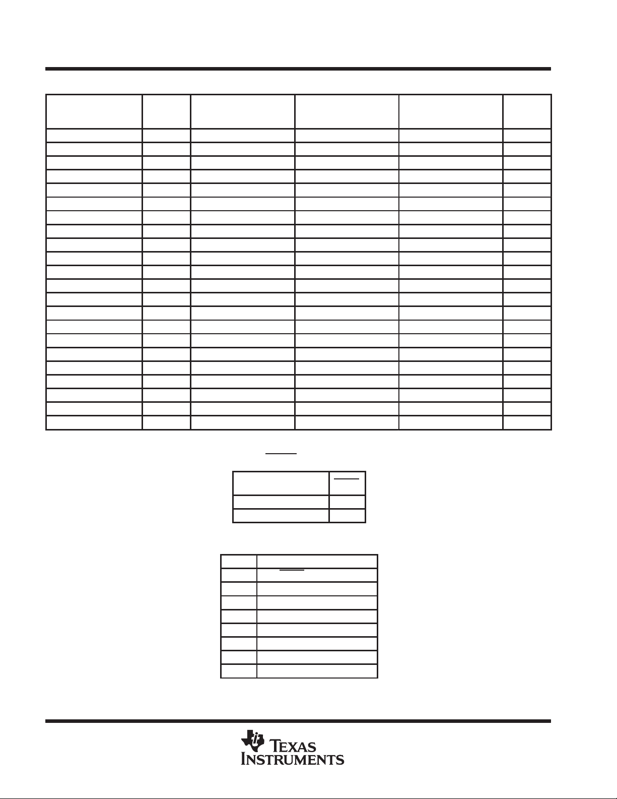
SCAS157D – APRIL 1990 – REVISED DECEMBER 1996
switching characteristics over recommended ranges of supply voltage and operating free-air
temperature (see Figure 9)
SN54ACT8997 SN74ACT8997
MIN MAX MIN MAX
z
2 14 3 12
2 16 3 14
7 28 9 25
7 26 9 24
7 27 9 25
7 26 9 24
9 31 11 29
9 31 12 29
4 21 6 19
5 23 7 21
5 23 7 20
5 22 7 20
3 17 5 15
3 16 4 14
5 19 5 17
5 20 7 18
6 23 7 21
6 28 9 26
6 23 9 21
6 24 9 22
8 30 10 27
8 31 10 28
9 31 11 28
9 33 11 30
8 31 11 29
10 35 13 33
9 37 14 35
8 35 13 32
max
t
PLH
t
PHL
t
PLH
t
PHL
t
PLH
t
PHL
t
PLH
t
PHL
PLH
PHL
t
PLH
t
PHL
t
PLH
t
PHL
PLH
PHL
t
PHZ
t
PLZ
t
PHZ
t
PLZ
t
PHZ
t
PLZ
t
PHZ
t
PLZ
t
PZH
t
PZL
t
PZH
t
PZL
t
PZH
t
PZL
t
PZH
t
PZL
FROM TO
(INPUT) (OUTPUT)
TCK 20 20
DCI (count mode) 20 20
DCO (open drain) 9 33 12 31
DCO (3 state) 9 32 12 30
DCO (open drain) 9 34 12 32
DCO (3 state) 9 31 12 29
DCO (open drain) 9 30 11 27
DCO (3 state) 6 29 10 26
DCO (open drain) 7 29 10 25
DCO (3 state) 6 26 9 23
POST OFFICE BOX 655303 • DALLAS, TEXAS 75265
21

SN54ACT8997, SN74ACT8997
SCAN-PATH LINKERS WITH 4-BIT IDENTIFICATION BUSES
SCAN-CONTROLLED IEEE STD 1149.1 (JTAG) TAP CONCATENATORS
SCAS157D – APRIL 1990 – REVISED DECEMBER 1996
APPLICATION INFORMATION
Subsystem
TDI TDO
SSP4
TDI TDO
SSP3
TDI TDO
SSP2
TDI TDO
SSP1
TCK
TMS
TCK
TMS
TCK
TMS
TCK
TMS
444
VCC or GND
VCC or GND
VCC or GND
VCC or GND
RSTOUT
PBC
TMSOUT
TCKOUT
TDO
INT1
INT2
TDI
DCI
MCO
ID1
ID2
ID3
ID4
(1–4)
DTDO
TDI
DCO
’ACT8997
TRST
TMS
TCK
MCI
DTCK
DTMS(1–4)
TDO
DTDI(1–4)
To Remainder
of Primary
Scan Path
22
POST OFFICE BOX 655303 • DALLAS, TEXAS 75265

From Output
Under Test
CL = 50 pF
(see Note A)
Input
SCAN-PATH LINKERS WITH 4-BIT IDENTIFICATION BUSES
SCAN-CONTROLLED IEEE STD 1149.1 (JTAG) TAP CONCATENATORS
PARAMETER MEASUREMENT INFORMATION
500 Ω
500 Ω
LOAD CIRCUIT
t
w
1.5 V 1.5 V
VOLTAGE WAVEFORMS
PULSE DURATION
S1
2 × V
GND
3 V
0 V
CC
Open
Timing Input
Data Input
SN54ACT8997, SN74ACT8997
SCAS157D – APRIL 1990 – REVISED DECEMBER 1996
TEST S1
t
PLH/tPHL
t
PLZ/tPZL
t
PHZ/tPZH
t
su
1.5 V
VOLTAGE WAVEFORMS
SETUP AND HOLD TIMES
1.5 V
Open
2 × V
GND
CC
t
h
1.5 V
3 V
0 V
3 V
0 V
Input
t
PLH
In-Phase
Output
t
PHL
Out-of-Phase
Output
PROPAGATION DELAY TIMES
NOTES: A. CL includes probe and jig capacitance.
B. Waveform 1 is for an output with internal conditions such that the output is low except when disabled by the output control.
Waveform 2 is for an output with internal conditions such that the output is high except when disabled by the output control.
C. Input pulses are supplied by generators having the following characteristics: PRR ≤ 10 MHz, ZO = 50 Ω, tr = 3 ns, tf = 3 ns.
For testing pulse duration: tr = 1 to 3 ns, tf = 1 to 3 ns. Pulse polarity may be either high-to-low-to-high or a low-to-high-to-low.
D. The outputs are measured one at a time with one transition per measurement.
1.5 V 1.5 V
50% V
CC
50% V
CC
VOLTAGE WAVEFORMS
Figure 9. Load Circuit and Voltage Waveforms
t
PHL
50% V
t
PLH
50% V
CC
CC
3 V
0 V
V
V
V
V
OH
OL
OH
OL
Output
Control
(low-level
enabling)
Output
Waveform 1
S1 at 2 × V
(see Note B)
Output
Waveform 2
S1 at GND
(see Note B)
CC
1.5 V
t
PZL
t
PLZ
50% V
CC
t
t
PZH
VOLTAGE WAVEFORMS
ENABLE AND DISABLE TIMES
PHZ
50% V
CC
1.5 V
20% V
80% V
CC
CC
3 V
0 V
[
V
V
[
V
OL
OH
0 V
CC
POST OFFICE BOX 655303 • DALLAS, TEXAS 75265
23

IMPORTANT NOTICE
T exas Instruments and its subsidiaries (TI) reserve the right to make changes to their products or to discontinue
any product or service without notice, and advise customers to obtain the latest version of relevant information
to verify, before placing orders, that information being relied on is current and complete. All products are sold
subject to the terms and conditions of sale supplied at the time of order acknowledgement, including those
pertaining to warranty, patent infringement, and limitation of liability.
TI warrants performance of its semiconductor products to the specifications applicable at the time of sale in
accordance with TI’s standard warranty. Testing and other quality control techniques are utilized to the extent
TI deems necessary to support this warranty . Specific testing of all parameters of each device is not necessarily
performed, except those mandated by government requirements.
CERTAIN APPLICATIONS USING SEMICONDUCTOR PRODUCTS MAY INVOLVE POTENTIAL RISKS OF
DEATH, PERSONAL INJURY, OR SEVERE PROPERTY OR ENVIRONMENTAL DAMAGE (“CRITICAL
APPLICATIONS”). TI SEMICONDUCTOR PRODUCTS ARE NOT DESIGNED, AUTHORIZED, OR
WARRANTED TO BE SUITABLE FOR USE IN LIFE-SUPPORT DEVICES OR SYSTEMS OR OTHER
CRITICAL APPLICA TIONS. INCLUSION OF TI PRODUCTS IN SUCH APPLICATIONS IS UNDERST OOD TO
BE FULLY AT THE CUSTOMER’S RISK.
In order to minimize risks associated with the customer’s applications, adequate design and operating
safeguards must be provided by the customer to minimize inherent or procedural hazards.
TI assumes no liability for applications assistance or customer product design. TI does not warrant or represent
that any license, either express or implied, is granted under any patent right, copyright, mask work right, or other
intellectual property right of TI covering or relating to any combination, machine, or process in which such
semiconductor products or services might be or are used. TI’s publication of information regarding any third
party’s products or services does not constitute TI’s approval, warranty or endorsement thereof.
Copyright 1998, Texas Instruments Incorporated
 Loading...