

Texas Instruments SN74ACT7882-15FN, SN74ACT7882-15PN, SN74ACT7882-20FN, SN74ACT7882-20PN, SN74ACT7882-30FN Datasheet
...
SN74ACT7882
2048 × 18
CLOCKED FIRST-IN, FIRST-OUT MEMORY
SCAS445C – JUNE 1994 – REVISED APRIL 1998
1
POST OFFICE BOX 655303 • DALLAS, TEXAS 75265
D
Member of the Texas Instruments
Widebus Family
D
Independent Asynchronous Inputs and
Outputs
D
Read and Write Operations Can Be
Synchronized to Independent System
Clocks
D
Programmable Almost-Full/Almost-Empty
Flag
D
Pin-to-Pin Compatible With SN74ACT7881
and SN74ACT7811
D
Input-Ready, Output-Ready, and Half-Full
Flags
D
Cascadable in Word Width and/or Word
Depth (See Application Information)
D
Fast Access Times of 11 ns With a 50-pF
Load
D
High Output Drive for Direct Bus Interface
D
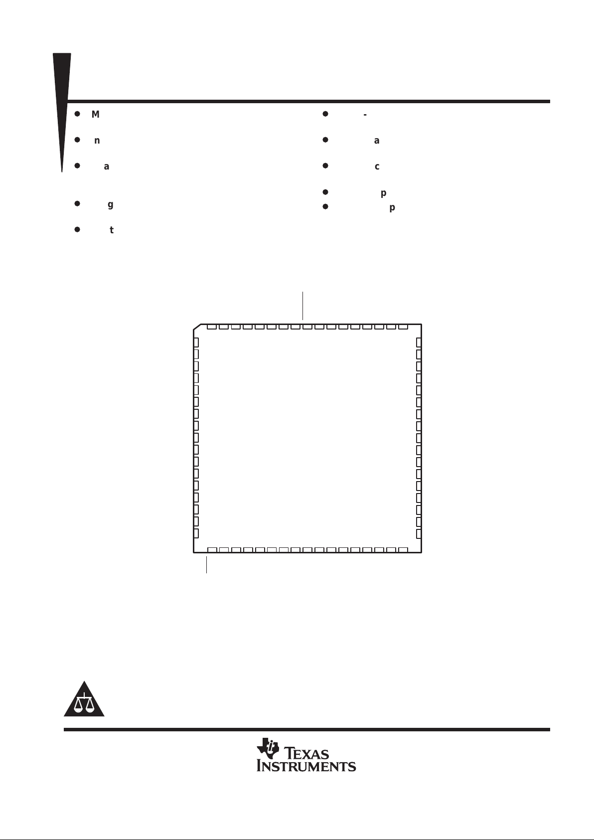
Package Options Include 68-Pin Plastic
Leaded Chip Carriers (FN) or 80-Pin Shrink
Quad Flat (PN) Package
28 29
V
CC
Q14
Q13
GND
Q12
Q11
V
CC
Q10
Q9
GND
Q8
Q7
V
CC
Q6
Q5
GND
Q4
60
59
58
57
56
55
54
53
52
51
50
49
48
47
46
45
44
30
10
11
12
13
14
15
16
17
18
19
20
21
22
23
24
25
26
D14
D13
D12
D11
D10
D9
V
CC
D8
GND
D7
D6
D5
D4
D3
D2
D1
D0
31 32 33 34
V
GND
87 65493
D17
GND
RDCLK
RDEN1
RDEN2OERESET
HF
Q0
Q1
WRTCLK
WRTEN1
WRTEN2
AF/AE
GND
IR
168672
35 36 37 38 39
66 65
27
DAF
GND
OR
V
64 63 62 61
40 41 42 43
GND
Q2
Q3
Q17
Q16
GND
Q15
D15
D16
CC
CC
FN PACKAGE
(TOP VIEW)
V
CC
V
CC
V
CC
Copyright 1998, Texas Instruments Incorporated
PRODUCTION DATA information is current as of publication date.
Products conform to specifications per the terms of Texas Instruments
standard warranty. Production processing does not necessarily include
testing of all parameters.
Please be aware that an important notice concerning availability, standard warranty, and use in critical applications of
Texas Instruments semiconductor products and disclaimers thereto appears at the end of this data sheet.
Widebus is a trademark of Texas Instruments Incorporated.
SN74ACT7882
2048 × 18
CLOCKED FIRST-IN, FIRST-OUT MEMORY
SCAS445C – JUNE 1994 – REVISED APRIL 1998
2
POST OFFICE BOX 655303 • DALLAS, TEXAS 75265
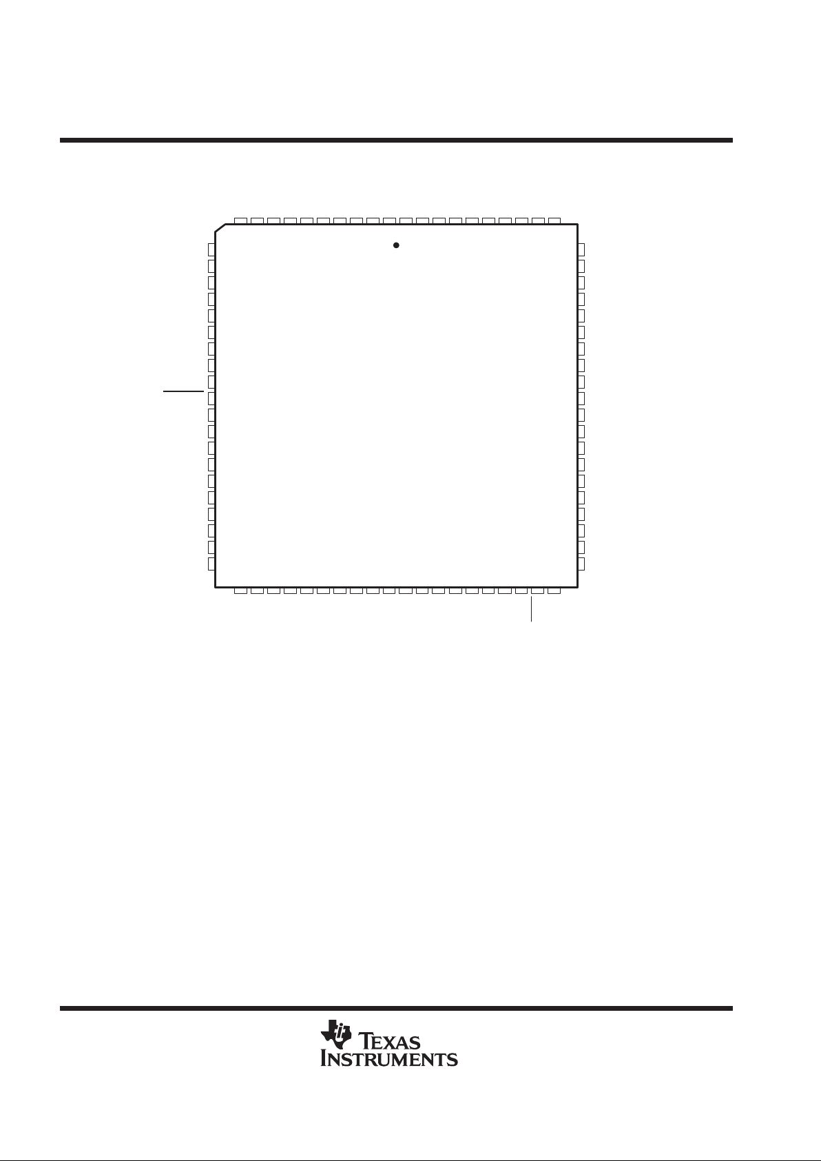
PN PACKAGE
(TOP VIEW)
22 23
V
CC
V
CC
NC
Q3
Q2
GND
Q1
Q0
V
CC
HF
IR
GND
GND
AF/AE
V
CC
WRTEN2
WRTEN1
WRTCLK
GND
NC
60
59
58
57
56
55
54
53
52
51
50
49
48
47
46
45
44
43
42
41
24
1
2
3
4
5
6
7
8
9
10
11
12
13
14
15
16
17
18
19
20
NC
GND
GND
Q16
Q17
V
CC
OR
GND
V
CC
RESET
OE
RDEN2
RDEN1
RDCLK
GND
D17
D16
D15
NC
NC
25 26 27 28
Q9
79 78 77 76 7580 74
Q14
Q13
GND
GND
Q12
Q11
D7
D5
D13
D12
D11
D10
D9VD8
72 71 7073
29
30 31 32 33
69 68
21
NC
Q8
67 66 65 64
34 35 36 37
D4D3D2
D1
Q7
Q6
Q5
Q15
Q10
D0
DAF
38 39 40
GND
GND
63 62 61
V
CC
GND
Q4
D14
D6
NC
CC
GND
V
CC
V
CC
NC – No internal connection
description
A FIFO memory is a storage device that allows data to be written into and read from its array at independent
data rates. The SN74ACT7882 is organized as 2048 bits deep × 18 bits wide. The SN74ACT7882 processes
data at rates up to 67 MHz and access times of 1 1 ns in a bit-parallel format. Data outputs are noninverting with
respect to the data inputs. Expansion is accomplished easily in both word width and word depth.
The SN74ACT7882 has normal input-bus to output-bus asynchronous operation. The special enable circuitry
adds the ability to synchronize independent reads and writes to their respective system clocks.
The SN74ACT7882 is characterized for operation from 0°C to 70°C.
SN74ACT7882
2048 × 18
CLOCKED FIRST-IN, FIRST-OUT MEMORY
SCAS445C – JUNE 1994 – REVISED APRIL 1998
3
POST OFFICE BOX 655303 • DALLAS, TEXAS 75265
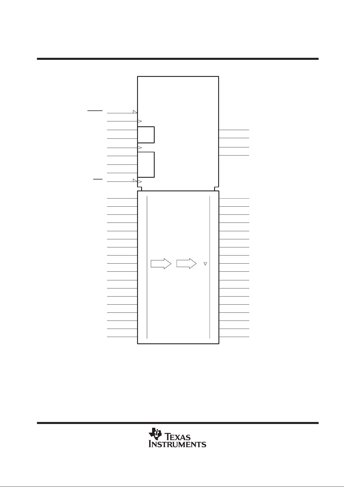
logic symbol
†
RESET
1
0
26
D0
25
D1
24
D2
23
D3
22
D4
9
D15
8
D16
17
7
D17
Q0
38
0
Q1
39
Q2
41
Q3
42
Q4
44
Q15
61
Q16
63
Q17
64
17
IR
35
IN RDY
21
D5
20
D6
19
D7
17
D8
15
D9
Q5
46
Q6
47
Q7
49
Q8
50
Q9
52
14
D10
13
D11
12
D12
11
D13
10
D14
Q10
53
Q11
55
Q12
56
Q13
58
Q14
59
Φ
FIFO
SN74ACT7882 – 2048 × 18
Data Data
1
29
WRTCLK
30
WRTEN1
31
WRTEN2
4
RDEN1
EN1
2
OE
3
RDEN2
RDCLK
WRTCLK
27
DEF ALMOST FULL
&
&
WRTEN
RDEN
RESET
DAF
HF
36
HALF FULL
AF/AE
33
ALMOST FULL/EMPTY
OR
66
OUT RDY
5
RDCLK
†
This symbol is in accordance with ANSI/IEEE Std 91-1984 and IEC Publication 617-12.
Pin numbers shown are for the FN package.
SN74ACT7882
2048 × 18
CLOCKED FIRST-IN, FIRST-OUT MEMORY
SCAS445C – JUNE 1994 – REVISED APRIL 1998
4
POST OFFICE BOX 655303 • DALLAS, TEXAS 75265
functional block diagram
RESET
•
•
Synchronous
Read
Control
Synchronous
Write
Control
Reset Logic
Read
Pointer
Status-
Flag
Logic
Location 1
Location 2
RAM
2048 × 18
Register
DAF
WRTEN2
WRTEN1
WRTCLK
RDEN2
RDEN1
RDCLK
D0–D17
OE
Q0–Q17
OR
IR
HF
AF/AE
Write
Pointer
SN74ACT7882
2048 × 18
CLOCKED FIRST-IN, FIRST-OUT MEMORY
SCAS445C – JUNE 1994 – REVISED APRIL 1998
5
POST OFFICE BOX 655303 • DALLAS, TEXAS 75265
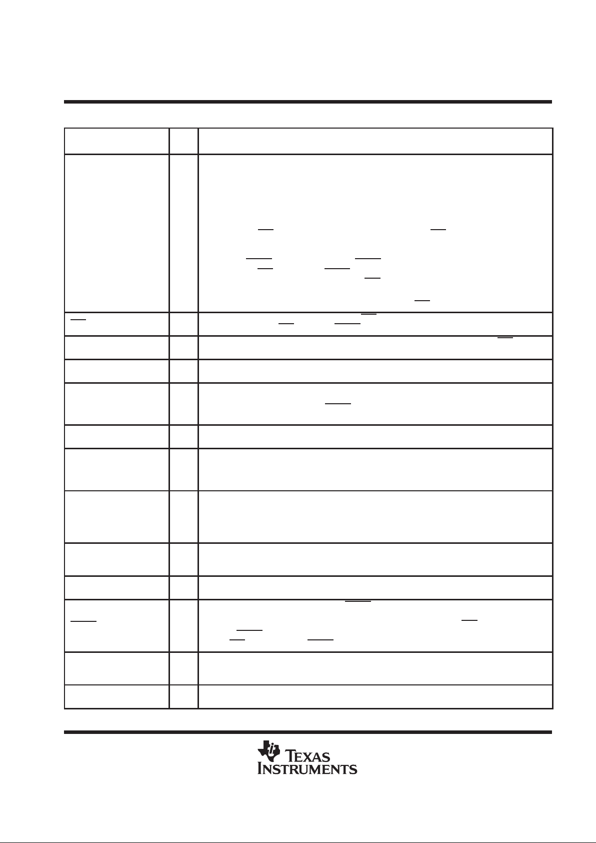
Terminal Functions
†
TERMINAL
NAME NO.
I/O
DESCRIPTION
AF/AE 33 O
Almost-full/almost-empty flag. The AF/AE boundary is defined by the AF/AE offset value (X). This
value can be programmed during reset or the default value of 256 can be used. AF/AE is high when
the number of words in memory is less than or equal to X. AF/AE also is high when the number of words
in memory is greater than or equal to (2048 – X).
Programming the AF/AE offset value (X) is accomplished during a reset cycle. The AF/AE offset value
(X) is either user-defined or the default value of X = 256. The procedure to program AF/AE is as follows:
User-defined X
Step 1: Take DAF
from high to low. The high-to-low transition of DAF input stores the binary value
on the data inputs as X. The following bits are used, listed from most significant bit to least significant
bit D9–D0.
Step 2: If RESET
is not already low, take RESET low.
Step 3: With DAF
held low, take RESET high. This defines the AF/AE using X.
NOTE: To retain the current (X) offset, keep DAF
low during subsequent reset cycles.
Default X
To redefine AF/AE using the default value of X = 256, hold DAF high during the reset cycle.
DAF
27 I
Define almost-full. The high-to-low transition of DAF stores the binary value of data inputs as the AF/AE
offset value (X). With DAF
held low, a RESET cycle defines the AF/AE flag using X.
D0–D17
26–19, 17,
15–7
I
Data inputs for 18-bit-wide data to be stored in the memory. A high-to-low transition on DAF captures
data for the almost-empty/almost-full offset (X) from D9–D0.
HF 36 O
Half-full flag. HF is high when the FIFO contains 1024 or more words and is low when the number of
words in memory is less than half the depth of the FIFO.
IR 35 O
Input-ready flag. IR is high when the FIFO is not full and low when the device is full. During reset, IR
is driven low on the rising edge of the second WRTCLK pulse. IR then is driven high on the rising edge
of the second WRTCLK pulse after RESET
goes high. After the FIFO is filled and IR is driven low, IR
is driven high on the second WRTCLK pulse after the first valid read.
OE 2 I
Output enable. The Q0–Q17 outputs are in the high-impedance state when OE is low. OE must be high
before the rising edge of RDCLK to read a word from memory.
OR 66 O
Output-ready flag. OR is high when the FIFO is not empty and low when it is empty . During reset, OR
is set low on the rising edge of the third RDCLK pulse. OR is set high on the rising edge of the third
RDCLK pulse to occur after the first word is written into the FIFO. OR is set low on the rising edge of
the first RDCLK pulse after the last word is read.
Q0–Q17
38–39, 41–42,
44, 46–47,
49–50, 52–53,
55–56, 58–59,
61, 63–64
O
Data out. The first data word to be loaded into the FIFO is moved to Q0–Q17 on the rising edge of the
third RDCLK pulse to occur after the first valid write. RDEN1 and RDEN2 do not affect this operation.
Following data is unloaded on the rising edge of RDCLK when RDEN1, RDEN2, OE, and OR are high.
RDCLK 5 I
Read clock. Data is read out of memory on the low-to-high transition at RDCLK if OR, OE, and RDEN1
and RDEN2 are high. RDCLK is a free-running clock and functions as the synchronizing clock for all
data transfers out of the FIFO. OR also is driven synchronously with respect to RDCLK.
RDEN1
RDEN2
4
3
I
Read enable. RDEN1 and RDEN2 must be high before a rising edge on RDCLK to read a word out
of memory. RDEN1 and RDEN2 are not used to read the first word stored in memory.
RESET
1 I
Reset. A reset is accomplished by taking RESET low and generating a minimum of four RDCLK and
WRTCLK cycles. This ensures that the internal read and write pointers are reset and that OR, HF , and
IR are low, and AF/AE is high. The FIFO must be reset upon power up. With DAF
at a low level, a low
pulse on RESET
defines AF/AE using the AF/AE offset value (X), where X is the value previously
stored. DAF
held high during a RESET cycle defines the AF/AE flag using the default value of X = 256.
WRTCLK 29 I
Write clock. Data is written into memory on a low-to-high transition of WRTCLK if IR, WRTEN1, and
WRTEN2 are high. WRTCLK is a free-running clock and functions as the synchronizing clock for all
data transfers into the FIFO. IR also is driven synchronously with respect to WRTCLK.
WRTEN1
WRTEN2
30
31
I
Write enable. WRTEN1 and WRTEN2 must be high before a rising edge on WRTCLK for a word to
be written into memory. WR TEN1 and WRTEN2 do not affect the storage of the AF/AE offset value (X).
†
Terminals listed are for the FN package.
 Loading...