

Datasheet SN74ACT7811-15FN, SN74ACT7811-15PN, SN74ACT7811-18FN, SN74ACT7811-18FNR, SN74ACT7811-18PN Datasheet (Texas Instruments)
...
SN74ACT7811
1024 × 18
CLOCKED FIRST-IN, FIRST-OUT MEMORY
SCAS151C – JANUARY 1991 – REVISED FEBRUARY 1996
1
POST OFFICE BOX 655303 • DALLAS, TEXAS 75265
D
Member of the Texas Instruments
Widebus Family
D
Independent Asynchronous Inputs and
Outputs
D
1024 Words × 18 Bits
D
Read and Write Operations Can Be
Synchronized to Independent System
Clocks
D
Programmable Almost-Full/Almost-Empty
Flag
D
Pin-to-Pin Compatible With SN74ACT7881,
SN74ACT7882, and SN74ACT7884
D
Input-Ready, Output-Ready, and Half-Full
Flags
D
Cascadable in Word Width and/or Word
Depth
D
Fast Access Times of 15 ns With a 50-pF
Load
D
High-Output Drive for Direct Bus Interface
D
Available in 68-Pin PLCC (FN) and
Space-Saving 80-Pin Thin Quad Flat (PN)
Packages
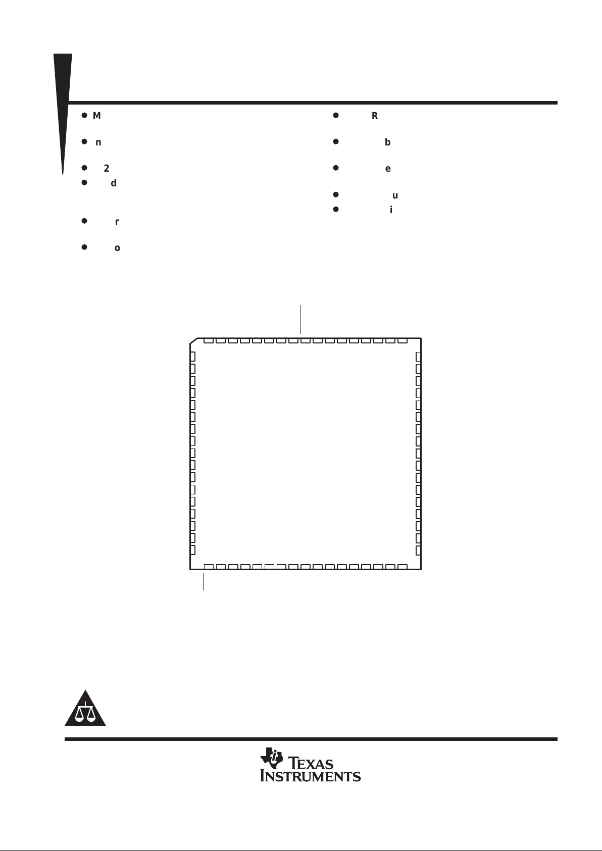
28 29
V
CC
Q14
Q13
GND
Q12
Q11
V
CC
Q10
Q9
GND
Q8
Q7
V
CC
Q6
Q5
GND
Q4
60
59
58
57
56
55
54
53
52
51
50
49
48
47
46
45
44
30
10
11
12
13
14
15
16
17
18
19
20
21
22
23
24
25
26
D14
D13
D12
D11
D10
D9
V
CC
D8
GND
D7
D6
D5
D4
D3
D2
D1
D0
31 32 33 34
V
GND
87 65493
D17
GND
RDCLK
RDEN1
RDEN2OERESET
HF
V
Q0
Q1
WRTCLK
WRTEN1
WRTEN2
AF/AE
GND
IR
168672
35 36 37 38 39
66 65
27
DAF
GND
OR
V
64 63 62 61
40 41 42 43
GND
Q2
Q3
V
Q17
Q16
GND
Q15
D15
D16
CC
CC
CC
CC
V
CC
FN PACKAGE
(TOP VIEW)
Copyright 1996, Texas Instruments Incorporated
PRODUCTION DATA information is current as of publication date.
Products conform to specifications per the terms of Texas Instruments
standard warranty. Production processing does not necessarily include
testing of all parameters.
Widebus is a trademark of Texas Instruments Incorporated.
Please be aware that an important notice concerning availability, standard warranty, and use in critical applications of
Texas Instruments semiconductor products and disclaimers thereto appears at the end of this data sheet.
SN74ACT7811
1024 × 18
CLOCKED FIRST-IN, FIRST-OUT MEMORY
SCAS151C – JANUARY 1991 – REVISED FEBRUARY 1996
2
POST OFFICE BOX 655303 • DALLAS, TEXAS 75265
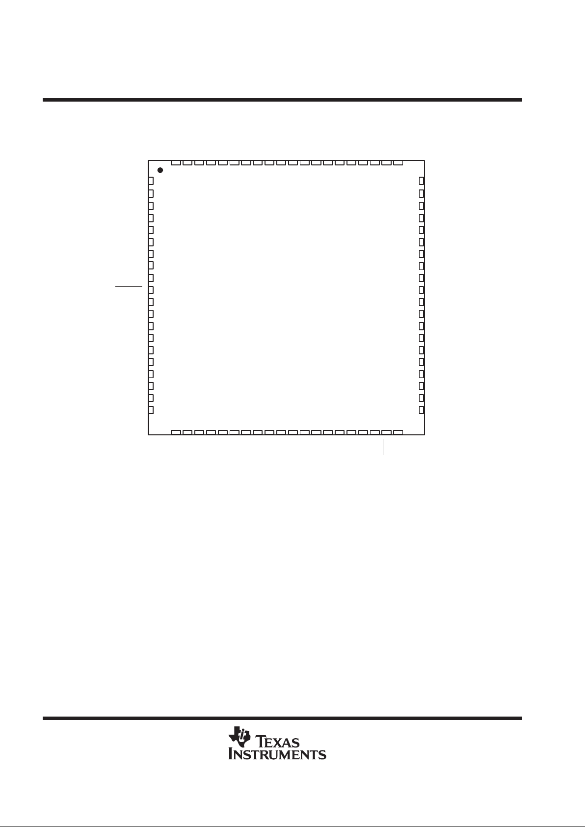
1
2
3
4
5
6
7
8
9
10
11
12
13
14
15
16
17
18
19
20
21 22 23 24 25
60
59
58
57
56
55
54
53
52
51
50
48
49
47
46
45
44
43
42
41
4026 27 28 29 30 31 32 33 34 35 36 37 38 39
80 79 78 77 76 75 74 73 71 70 69 68 67 66 65 64 63 62 6172
NC
GND
GND
NC
NC
NC
NC
V
CC
NC
GND
Q16
Q17
OR
GND
V
CC
OE
RDEN2
RDEN1
RDCLK
D14
D16
D15
GND
D17
RESET
V
CC
GND
NC
D13
D12
D11
D10
D9
D8
D7D6D5D4D3D2D1
D0
DAF
V
CC
V
CC
GND
V
CC
GND
GND
V
CC
WRTCLK
WRTEN1
WRTEN2
AF/AE
IR
HF
Q1
Q0
Q2
Q3
Q4
Q5
GND
GND
Q6
Q7
V
CC
Q8
GND
Q9
Q10
Q11
V
CC
Q12
Q13
GND
GND
Q14
V
CC
Q15
PN PACKAGE
(TOP VIEW)
NC – No internal connection
description
A FIFO memory is a storage device that allows data to be written into and read from its array at independent
data rates. The SN74ACT781 1 is a 1024 × 18-bit FIFO for high speed and fast access times. It processes data
at rates up to 40 MHz and access times of 15 ns in a bit-parallel format. Data outputs are noninverting with
respect to the data inputs. Expansion is easily accomplished in both word width and word depth.
The SN74ACT781 1 has normal input-bus-to-output-bus asynchronous operation. The special enable circuitry
adds the ability to synchronize independent read and write (interrupts or requests) to their respective system
clock.
The SN74ACT7811 is characterized for operation from 0°C to 70°C.
SN74ACT7811
1024 × 18
CLOCKED FIRST-IN, FIRST-OUT MEMORY
SCAS151C – JANUARY 1991 – REVISED FEBRUARY 1996
3
POST OFFICE BOX 655303 • DALLAS, TEXAS 75265
logic symbol
†
3
1
29
30
31
5
4
&
RDCLK
14
D10
13
D11
12
D12
11
D13
10
D14
9
D15
8
D16
17
7
D17
RESET
WRTCLK
WRTEN1
WRTEN2
RDCLK
RDEN1
RDEN2
&
RDEN
WRTCLK
EN1
2
OE
0
26
D0
25
D1
24
D2
23
D3
22
D4
21
D5
20
D6
19
D7
17
D8
15
D9
WRTEN
Data
Q0
38
0
Q1
39
Q2
41
Q3
42
Q4
44
IR
35
IN RDY
HF
36
HALF FULL
AF/AE
33
ALMOST FULL/EMPTY
OR
66
OUT RDY
Q15
61
Q16
63
Q17
64
17
Q5
46
Q6
47
Q7
49
Q8
50
Q9
52
Q10
53
Q11
55
Q12
56
Q13
58
Q14
59
1
DEF ALMOST FULL
27
Φ
FIFO 1024 × 18
SN74ACT7811
DAF
RESET
Data
†
This symbol is in accordance with ANSI/IEEE Std 91-1984 and IEC Publication 617-12.
Pin numbers shown are for the FN package.
SN74ACT7811
1024 × 18
CLOCKED FIRST-IN, FIRST-OUT MEMORY
SCAS151C – JANUARY 1991 – REVISED FEBRUARY 1996
4
POST OFFICE BOX 655303 • DALLAS, TEXAS 75265
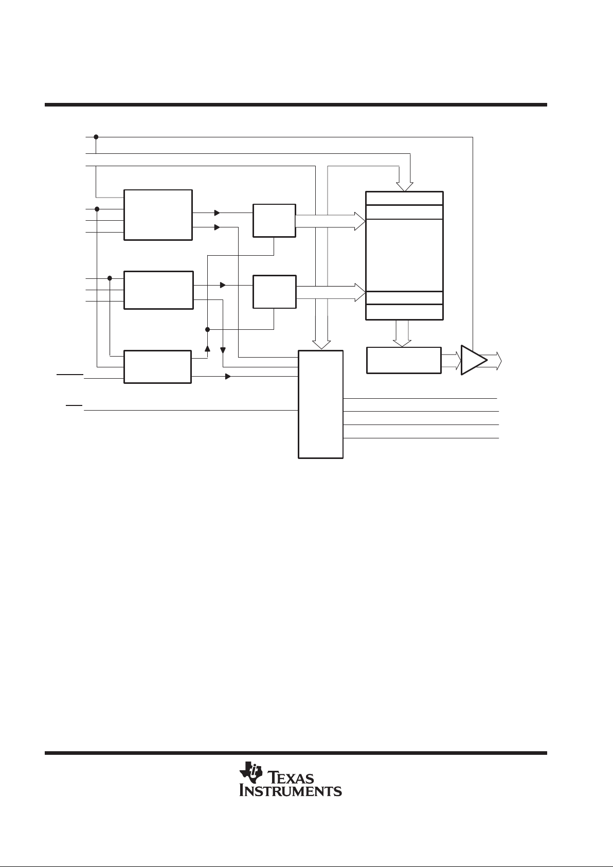
functional block diagram
Write
Read
Location 1
Location 2
Location 1024
Location 1023
Pointer
Pointer
Synchronous
Synchronous
Write
Control
Read
Control
Reset
Logic
OE
D0 – D17
WRTCLK
WRTEN1
WRTEN2
Q0 – Q17
OR
IR
AF/AE
HF
RDCLK
RDEN1
RDEN2
Flag
Status-
Logic
DAF
Register
RESET
1024 × 18 RAM
SN74ACT7811
1024 × 18
CLOCKED FIRST-IN, FIRST-OUT MEMORY
SCAS151C – JANUARY 1991 – REVISED FEBRUARY 1996
5
POST OFFICE BOX 655303 • DALLAS, TEXAS 75265
Terminal Functions
TERMINAL
†
NAME NO.
I/O
DESCRIPTION
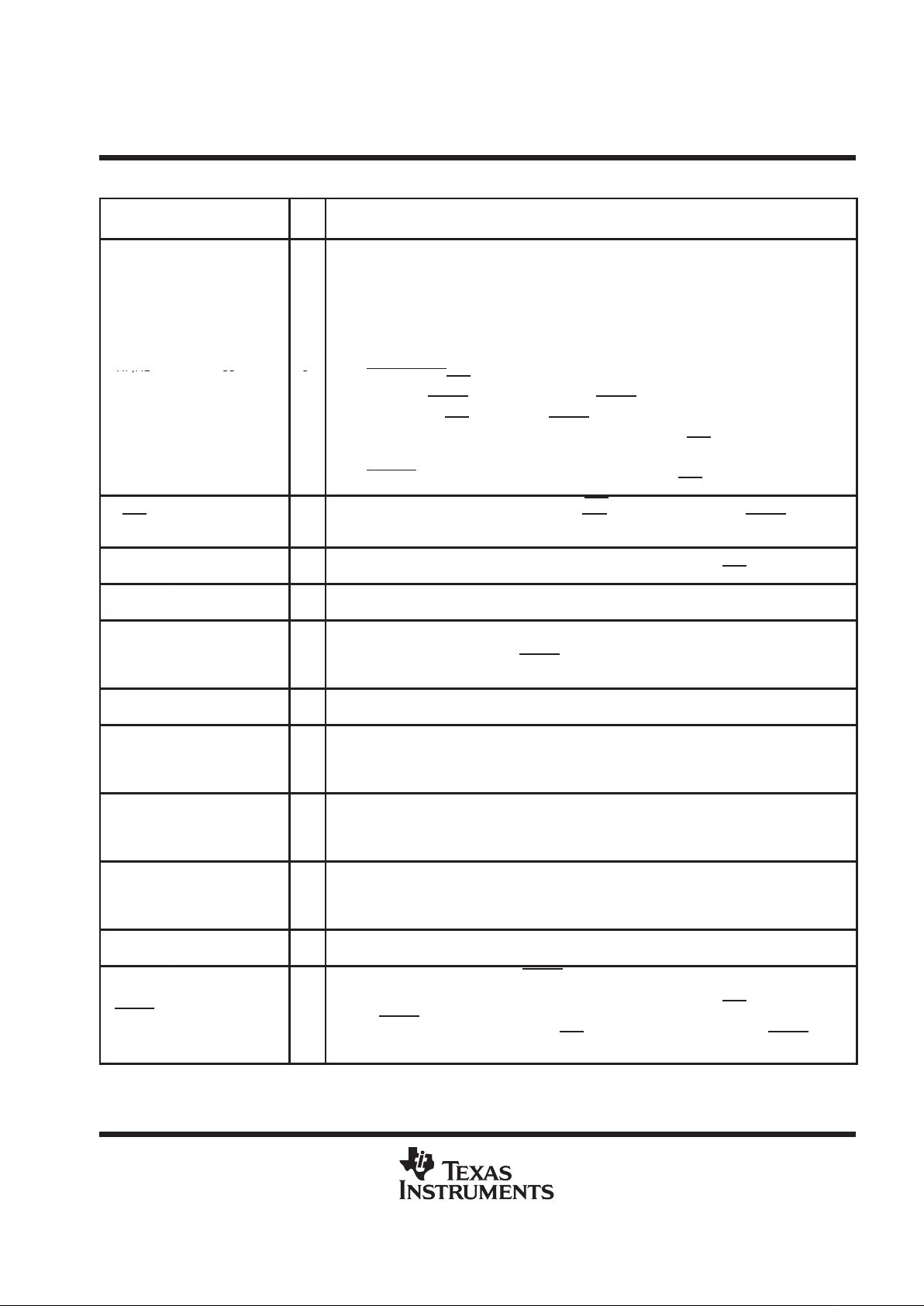
Almost-full/almost-empty flag. The AF/AE boundary is defined by the almost-full/almost-empty offset
value (X). This value can be programmed during reset or the default value of 256 can be used. AF/AE
is high when the FIFO contains (X + 1) or less words or (1025 – X) or more words. AF/AE is low when
the FIFO contains between (X +2) and (1024 - X) words.
Programming procedure for AF/AE – The almost-full/almost-empty flag is programmed during each
reset cycle. The almost-full/almost-empty offset value (X) is either a user-defined value or the default
of X = 256. Instructions to program AF/AE using both methods are as follows:
AF/AE 33 O
User-defined X
AF/AE
33
O
Step 1:
Take DAF
from high to low.
Step 2:
If RESET is not already low, take RESET low.
Step 3:
With DAF held low, take RESET high. This defines the AF/AE using X.
Step 4:
To retain the current offset for the next reset, keep DAF low.
Default X
To redefine AF/AE using the default value of X = 256, hold DAF high during the reset cycle.
DAF 27 I
Define almost full. The high-to-low transition of DAF stores the binary value of data inputs as the
almost-full/almost-empty offset value (X). With DAF
held low, a low pulse on RESET defines the
AF/AE flag using X.
D0–D17
26–19, 17, 15–7 I
Data inputs for 18-bit-wide data to be stored in the memory. Data lines D0– D8 also carry the
almost-full/almost-empty offset value (X) on a high-to-low transition of the DAF
.
HF 36 O
Half-full flag. HF is high when the FIFO contains 513 or more words and is low when it contains 512
or less words.
IR 35 O
Input-ready flag. IR is high when the FIFO is not full and low when the device is full. During reset, IR
is driven low on the rising edge of the second WRTCLK pulse. IR is then driven high on the rising edge
of the second WRTCLK pulse after RESET
goes high. After the FIFO is filled and IR is driven low,
IR is driven high on the second WRTCLK pulse after the first valid read.
OE 2 I
Output enable. The data-out (Q0–Q17) outputs are in the high-impedance state when OE is low. OE
must be high before the rising edge of RDCLK to read a word from memory.
OR 66 O
Output-ready flag. OR is high when the FIFO is not empty and low when it is empty. During reset,
OR is set low on the rising edge of the third RDCLK pulse. OR is set high on the rising edge of the
third RDCLK pulse to occur after the first word is written into the FIFO. OR is set low on the rising
edge of the first RDCLK pulse after the last word is read.
Q0–Q17
38–39, 41–42, 44,
46–47, 49–50,
52–53, 55–56,
58–59, 61, 63–64
O
Data outputs. The first data word to be loaded into the FIFO is moved to Q0–Q17 on the rising edge
of the third RDCLK pulse to occur after the first valid write. The RDEN1 and RDEN2 inputs do not
affect this operation. Following data is unloaded on the rising edge of RDCLK when RDEN1, RDEN2,
OE, and the OR are high.
RDCLK 5 I
Read clock. Data is read out of memory on a low-to-high transition RDCLK if OR, OE, and RDEN1
and RDEN2 control inputs are high. RDCLK is a free-running clock and functions as the
synchronizing clock for all data transfers out of the FIFO. OR is also driven synchronously with
respect to RDCLK.
RDEN1,
RDEN2
4
3
I
Read enable. RDEN1 and RDEN2 must be high before a rising edge on RDCLK to read a word out
of memory. RDEN1 and RDEN2 are not used to read the first word stored in memory.
RESET 1 I
A reset is accomplished by taking RESET low and generating a minimum of four RDCLK and
WRTCLK cycles. This ensures that the internal read and write pointers are reset and OR, HF, and
IR are low and AF/AE is high. The FIFO must be reset upon power up. With DAF
at a low level, a low
pulse on RESET
defines the AF/AE status flag using the almost-full/almost-empty offset value (X),
where X is the value previously stored. With DAF
at a high level, a low-level pulse on RESET defines
the AF/AE flag using the default value of X = 256.
†
Terminals listed are for the FN package.
SN74ACT7811
1024 × 18
CLOCKED FIRST-IN, FIRST-OUT MEMORY
SCAS151C – JANUARY 1991 – REVISED FEBRUARY 1996
6
POST OFFICE BOX 655303 • DALLAS, TEXAS 75265
Terminal Functions (Continued)
TERMINAL
†
NAME NO.
I/O
DESCRIPTION
WRTCLK 29 I
Write clock. Data is written into memory on a low-to-high transition of WRTCLK if IR, WRTEN1, and
WRTEN2 are high. WRTCLK is a free-running clock and functions as the synchronizing clock for all
data transfers into the FIFO. IR is also driven synchronously with respect to WRTCLK.
WRTEN1,
WRTEN2
30
31
I
Write enables. WRTEN1 and WRTEN2 must be high before a rising edge on WRTCLK for a word
to be written into memory. WRTEN1 and WRTEN2 do not affect the storage of the
almost-full/almost-empty offset value (X).
†
Terminals listed are for the FN package.
ОООООООО
12341
2
1234
Invalid
WRTCLK
WRTEN1
WRTEN2
D0 – D17
RDCLK
RDEN1
RDEN2
Q0 – Q17
OR
AF/AE
IR
Store the Value of D0–D8 as X
Define the AF/AE Flag Using the
Value of X
HF
OE
X
†
Don’t Care
Don’t Care
Don’t Care
Don’t Care
Don’t Care
Don’t Care
Don’t Care
Don’t Care
Don’t Care
Don’t Care
RESET
DAF
1
0
†
X is the binary value of D0–D8 only.
Figure 1. Reset Cycle: Define AF/AE Using the Value of X

SN74ACT7811
1024 × 18
CLOCKED FIRST-IN, FIRST-OUT MEMORY
SCAS151C – JANUARY 1991 – REVISED FEBRUARY 1996
7
POST OFFICE BOX 655303 • DALLAS, TEXAS 75265
12341
2
1234
Invalid
WRTCLK
WRTEN1
WRTEN2
D0 – D17
RDCLK
RDEN1
RDEN2
Q0 – Q17
OR
AF/AE
IR
Define the AF/AE Flag
Using the Value of X = 256
HF
OE
Don’t Care
Don’t Care
Don’t Care
Don’t Care
Don’t Care
Don’t Care
Don’t Care
Don’t Care
Don’t Care
Don’t Care
RESET
DAF
1
0
Figure 2. Reset Cycle: Define AF/AE Using the Default Value

SN74ACT7811
1024 × 18
CLOCKED FIRST-IN, FIRST-OUT MEMORY
SCAS151C – JANUARY 1991 – REVISED FEBRUARY 1996
8
POST OFFICE BOX 655303 • DALLAS, TEXAS 75265
123
Invalid
RESET
WRTCLK
DAF
WRTEN1
WRTEN2
D0–D17
RDCLK
RDEN1
OE
RDEN2
Q0–Q17
OR
AF/AE
HF
IR
1
0
1
0
W1 W2 W3 W4 W(X+2) W513 W(1025–X) W1025
1
0
1
0
W1
Don’t Care
Figure 3. Write Cycle

SN74ACT7811
1024 × 18
CLOCKED FIRST-IN, FIRST-OUT MEMORY
SCAS151C – JANUARY 1991 – REVISED FEBRUARY 1996
9
POST OFFICE BOX 655303 • DALLAS, TEXAS 75265
ЙЙЙЙЙЙЙЙЙЙЙЙЙЙЙЙЙЙЙЙЙЙЙЙЙЙЙЙЙ
W514
ООООООООООООООООООООООООООООО
RESET
WRTCLK
DAF
WRTEN1
WRTEN2
D0–D17
RDCLK
RDEN1
OE
RDEN2
Q0–Q17
OR
AF/AE
HF
IR
1
0
W1025
1
2
W1 W2 W3 W(X+1) W(X+2) W513 W(1024–X) W(1025–X) W1024 W1025
Don’t Care
W1
Figure 4. Read Cycle

SN74ACT7811
1024 × 18
CLOCKED FIRST-IN, FIRST-OUT MEMORY
SCAS151C – JANUARY 1991 – REVISED FEBRUARY 1996
10
POST OFFICE BOX 655303 • DALLAS, TEXAS 75265
absolute maximum ratings over operating free-air temperature range (unless otherwise noted)
†
Supply voltage range, V
CC
–0.5 V to 7 V. . . . . . . . . . . . . . . . . . . . . . . . . . . . . . . . . . . . . . . . . . . . . . . . . . . . . . . . . .
Input voltage, V
I
7 V. . . . . . . . . . . . . . . . . . . . . . . . . . . . . . . . . . . . . . . . . . . . . . . . . . . . . . . . . . . . . . . . . . . . . . . . . . . . .
Voltage applied to a disabled 3-state output 5.5 V. . . . . . . . . . . . . . . . . . . . . . . . . . . . . . . . . . . . . . . . . . . . . . . . . . .
Operating free-air temperature range, T
A
0°C to 70°C. . . . . . . . . . . . . . . . . . . . . . . . . . . . . . . . . . . . . . . . . . . . . . .
Storage temperature range, T
stg
–65°C to 150°C. . . . . . . . . . . . . . . . . . . . . . . . . . . . . . . . . . . . . . . . . . . . . . . . . . . .
†
Stresses beyond those listed under “absolute maximum ratings” may cause permanent damage to the device. These are stress ratings only, and
functional operation of the device at these or any other conditions beyond those indicated under “recommended operating conditions” is not
implied. Exposure to absolute-maximum-rated conditions for extended periods may affect device reliability.
recommended operating conditions
MIN MAX UNIT
V
CC
Supply voltage 4.5 5.5 V
V
IH
High-level input voltage 2 V
V
IL
Low-level input voltage 0.8 V
I
OH
High-level output current –8 mA
I
OL
Low-level output current 16 mA
T
A
Operating free-air temperature 0 70 °C
electrical characteristics over recommended operating free-air temperature range (unless
otherwise noted)
PARAMETER TEST CONDITIONS MIN TYP‡MAX UNIT
V
OH
VCC = 4.5 V, IOH = – 8 mA 2.4 V
V
OL
VCC = 4.5 V, IOL = 16 mA 0.5 V
I
I
VCC = 5.5 V, VI =VCC or 0 V ±5 µA
I
OZ
VCC = 5.5 V, VO =VCC or 0 V ±5 µA
VI =VCC – 0.2 V or 0 V 400 µA
I
CC
§
One input at 3.4 V , Other inputs at VCC or GND 1 mA
C
i
VI = 0 V, f = 1 MHz 4 pF
C
o
VO = 0 V, f = 1 MHz 8 pF
‡
All typical values are at VCC = 5 V, TA = 25°C.
§
ICC tested with outputs open

SN74ACT7811
1024 × 18
CLOCKED FIRST-IN, FIRST-OUT MEMORY
SCAS151C – JANUARY 1991 – REVISED FEBRUARY 1996
11
POST OFFICE BOX 655303 • DALLAS, TEXAS 75265
timing requirements (see Figures 1 through 8)
′ACT7811-15 ′ACT7811-18 ′ACT7811-20 ′ACT7811-25
MIN MAX MIN MAX MIN MAX MIN MAX
UNIT
f
clock
Clock frequency 40 35 28.5 16.7 MHz
D0–D17 high or low 10 12 14 20
WRTCLK high 7 8.5 10 17
WRTCLK low 10 11 14 23
RDCLK high 7 8.5 10 17
RDCLK low 10 11 14 23
twPulse duration
DAF high 10 10 10 10
ns
WRTEN1, WRTEN2
high or low
10 10 10 10
OE, RDEN1, RDEN2
high or low
10 10 10 10
D0–D17 before WRTCLK↑ 5 5 5 5
WRTEN1, WRTEN2 high
before WRTCLK↑
5 5 5 5
OE, RDEN1, RDEN2 high
before RDCLK↑
5 5 5 5
t
su
Setup time
Reset: RESET
low before first
WRTCLK and RDCLK↑
7 7 7 7
ns
Define AF/AE: D0–D8 before
DAF
↓
5 5 5 5
Define AF/AE: DAF↓ before
RESET
↑
7 7 7 7
Define AF/AE (default):
DAF
high before RESET↑
5 5 5 5
D0–D17 after WRTCLK↑ 1 1 1 1
WRTEN1, WRTEN2 high after
WRTCLK↑
1 1 1 1
OE, RDEN1, RDEN2 high after
RDCLK↑
1 1 1 1
t
h
Hold time
Reset: RESET
low after fourth
WRTCLK and RDCLK↑
0 0 0 0
ns
Define AF/AE: D0–D8 after
DAF
↓
1 1 1 1
Define AF/AE: DAF low after
RESET
↑
0 0 0 0
Define AF/AE (default):
DAF
high after RESET↑
1 1 1 1
†
To permit the clock pulse to be utilized for reset purposes

SN74ACT7811
1024 × 18
CLOCKED FIRST-IN, FIRST-OUT MEMORY
SCAS151C – JANUARY 1991 – REVISED FEBRUARY 1996
12
POST OFFICE BOX 655303 • DALLAS, TEXAS 75265
switching characteristics over recommended operating free-air temperature range (see Figures 9
and 10)
PARAMETER
FROM
(
INPUT
)
TO
(
OUTPUT
)
VCC = 4.5 V to 5.5 V,
CL = 50 pF,
RL = 500 Ω,
TA = 0°C to 70°C
UNIT
(INPUT)
(OUTPUT)
′ACT7811-15 ′ACT7811-18 ′ACT7811-20 ′ACT7811-25
MIN TYP MAX MIN MAX MIN MAX MIN MAX
f
max
WRTCLK or
RDCLK
40 35 28.5 16.7 MHz
t
pd
4 12 15 4 18 4 20 4 25
t
pd
†
RDCLK
↑
Any Q
10.5
ns
t
pd
WRTCLK↑ IR 2 10 2 12 2 14 2 16 ns
t
pd
RDCLK↑ OR 2 10 2 12 2 14 2 16 ns
WRTCLK↑
6 20 6 22 6 24 6 26
t
pd
RDCLK↑
AF/AE
6 20 6 22 6 24 6 26
ns
t
PLH
WRTCLK↑
6 19 6 21 6 23 6 25
t
PHL
RDCLK↑
HF
6 19 6 21 6 23 6 25
ns
t
PLH
AF/AE 3 19 3 21 3 23 3 25
t
PHL
RESET↓
HF 4 21 4 23 4 25 4 27
ns
t
en
2 11 2 11 2 11 2 11
t
dis
OE
Any Q
2 14 2 14 2 14 2 14
ns
†
This parameter is measured with CL = 30 pF (see Figure 5).
operating characteristics, VCC = 5 V, TA = 25°C
PARAMETER TEST CONDITIONS TYP UNIT
C
pd
Power dissipation capacitance per 1K bits CL = 50 pF, f = 5 MHz 65 pF

SN74ACT7811
1024 × 18
CLOCKED FIRST-IN, FIRST-OUT MEMORY
SCAS151C – JANUARY 1991 – REVISED FEBRUARY 1996
13
POST OFFICE BOX 655303 • DALLAS, TEXAS 75265
TYPICAL CHARACTERISTICS
Figure 2Figure 3Figure 4
14
12
11
10
16
17
TYPICAL PROPAGATION DELAY TIME
vs
LOAD CAPACITANCE
18
15
13
0 50 100 150 200 250 300
C – Load Capacitance – pF
L
t – Propagation Delay Time – ns
pd
VCC = 5 V
TA = 25°C
RL = 500 Ω
Figure 5

SN74ACT7811
1024 × 18
CLOCKED FIRST-IN, FIRST-OUT MEMORY
SCAS151C – JANUARY 1991 – REVISED FEBRUARY 1996
14
POST OFFICE BOX 655303 • DALLAS, TEXAS 75265
TYPICAL CHARACTERISTICS
65
64
63
62
4.5 4.6 4.7 4.8 4.9 5 5.1
66
67
TYPICAL POWER DISSIPATION CAPACITANCE
vs
SUPPLY VOLTAGE
68
5.2 5.3 5.4 5.5
VCC – Supply Voltage – V
– Power Dissipation Capacitance – pF
pd
fi = 5 MHz
TA = 25°C
CL = 50 pF
Figure 6
calculating power dissipation
The maximum power dissipation (PT) of the SN74ACT7811 can be calculated by:
P
T
= VCC × [ICC + (N × ∆ICC × dc)] + Σ (Cpd × V
CC
2
× fi) + Σ (CL × V
CC
2
× fo)
where:
I
CC
= power-down ICC maximum
N = number of inputs driven by a TTL device
∆ I
CC
= increase in supply current
dc = duty cycle of inputs at a TTL high level of 3.4 V
C
pd
= power dissipation capacitance
C
L
= output capacitive load
f
i
= data input frequency
f
o
= data output frequency

SN74ACT7811
1024 × 18
CLOCKED FIRST-IN, FIRST-OUT MEMORY
SCAS151C – JANUARY 1991 – REVISED FEBRUARY 1996
15
POST OFFICE BOX 655303 • DALLAS, TEXAS 75265
APPLICATION INFORMATION
expanding the SN74ACT7811
The SN74ACT7811 is expandable in width and depth. Expanding in word depth offers special timing
considerations:
After the first data word is loaded into the FIFO, the word is unloaded and the output-ready flag (OR) output
goes high after (N × 3) read-clock (RDCLK) cycles, where N is the number of devices used in depth
expansion.
After the FIFO is filled, the input-ready flag (IR) output goes low, the first word is unloaded, and the IR flag
output is driven high after (N × 2) write-clock cycles, where N is the number of devices used in depth
expansion.
WRTCLK
WRTEN1
WRTEN2
IR
WRTCLK
WRTEN1
WRTEN2
IR
D0 – D17D0 – D17
RDCLK
OR
RDEN1
RDEN2
OE
WRTCLK
WRTEN1
WRTEN2
IR
D0 – D17
RDCLK
OE
Q0 – Q17
Q0 – Q17
5 V
RDCLK
RDEN1RDEN1
RDEN2
OR
RDEN2
OR
OE
Q0 – Q17
CLOCK
SN74ACT7811 SN74ACT7811
Figure 7. Word-Depth Expansion: 2048 Words × 18 Bits, N = 2
WRTCLK
WRTEN1
WRTEN2
IR
D0 – D17
RDCLK
OE
Q0 – Q17
RDEN1
RDEN2
OR
WRTCLK
WRTEN1
WRTEN2
IR
D0 – D17
RDCLK
OE
Q0 – Q17
RDEN1
RDEN2
OR
WRTCLK
WRTEN
D18 – D35
IR
D0 – D17
RDCLK
RDEN
Q18 – Q35
OR
Q0 – Q17
OE
SN74ACT7811
SN74ACT7811
Figure 8. Word-Width Expansion: 1024 Words × 36 Bits

SN74ACT7811
1024 × 18
CLOCKED FIRST-IN, FIRST-OUT MEMORY
SCAS151C – JANUARY 1991 – REVISED FEBRUARY 1996
16
POST OFFICE BOX 655303 • DALLAS, TEXAS 75265
PARAMETER MEASUREMENT INFORMATION
From Output
Under Test
LOAD CIRCUIT
Input 1.5 V
Output
1.5 V
TOTEM-POLE OUTPUTS
3 V
3 V
0 V
0 V
t
pd
t
pd
RL = 500 Ω CL = 50 pF
Figure 9. Standard CMOS Outputs
S1
R2
C
L
LOAD CIRCUIT
Output
Output
1.5 V 1.5 V
≈ 3.5 V
V
OL
V
OH
0.3 V
≈ 0 V
t
PZL
t
PZH
t
PHZ
VOLTAGE WAVEFORMS
1.5 V
1.5 V
R1
0.3 V
7 V
3 V
0 V
From Output
Under Test
Test
Point
Input
RL = R1 = R2
t
PLZ
PARAMETER R1, R2 C
L
†
S1
t
PZH
p
Open
t
en
t
PZL
500 Ω
50 pF
Closed
t
PHZ
p
Open
t
dis
t
PLZ
500 Ω
50 pF
Closed
t
pd
500 Ω 50 pF Open
†
Includes probe and test fixture capacitanceFigure 9
Figure 10. 3-State Outputs (Any Q)

IMPORTANT NOTICE
T exas Instruments and its subsidiaries (TI) reserve the right to make changes to their products or to discontinue
any product or service without notice, and advise customers to obtain the latest version of relevant information
to verify, before placing orders, that information being relied on is current and complete. All products are sold
subject to the terms and conditions of sale supplied at the time of order acknowledgement, including those
pertaining to warranty, patent infringement, and limitation of liability.
TI warrants performance of its semiconductor products to the specifications applicable at the time of sale in
accordance with TI’s standard warranty. Testing and other quality control techniques are utilized to the extent
TI deems necessary to support this warranty. Specific testing of all parameters of each device is not necessarily
performed, except those mandated by government requirements.
CERT AIN APPLICATIONS USING SEMICONDUCTOR PRODUCTS MA Y INVOLVE POTENTIAL RISKS OF
DEATH, PERSONAL INJURY, OR SEVERE PROPERTY OR ENVIRONMENTAL DAMAGE (“CRITICAL
APPLICATIONS”). TI SEMICONDUCTOR PRODUCTS ARE NOT DESIGNED, AUTHORIZED, OR
WARRANTED TO BE SUITABLE FOR USE IN LIFE-SUPPORT DEVICES OR SYSTEMS OR OTHER
CRITICAL APPLICATIONS. INCLUSION OF TI PRODUCTS IN SUCH APPLICA TIONS IS UNDERST OOD TO
BE FULLY AT THE CUSTOMER’S RISK.
In order to minimize risks associated with the customer’s applications, adequate design and operating
safeguards must be provided by the customer to minimize inherent or procedural hazards.
TI assumes no liability for applications assistance or customer product design. TI does not warrant or represent
that any license, either express or implied, is granted under any patent right, copyright, mask work right, or other
intellectual property right of TI covering or relating to any combination, machine, or process in which such
semiconductor products or services might be or are used. TI’s publication of information regarding any third
party’s products or services does not constitute TI’s approval, warranty or endorsement thereof.
Copyright 1999, Texas Instruments Incorporated
 Loading...