

Datasheet SN74ACT2227DW, SN74ACT2227DWR, SN74ACT2229DW, SN74ACT2229DWR Datasheet (Texas Instruments)
SN74ACT2227, SN74ACT2229
DUAL 64 × 1, DUAL 256 × 1
FIRST-IN, FIRST-OUT MEMORIES
SCAS220C – JUNE 1992 – REVISED OCTOBER 1997
1
POST OFFICE BOX 655303 • DALLAS, TEXAS 75265
D
Dual Independent FIFOs Organized as:
64 Words by 1 Bit Each – SN74ACT2227
256 Words by 1 Bit Each – SN74ACT2229
D
Free-Running Read and Write Clocks Can
Be Asynchronous or Coincident on Each
FIFO
D
Input-Ready Flags Synchronized to Write
Clocks
D
Output-Ready Flags Synchronized to Read
Clocks
D
Half-Full and Almost-Full/Almost-Empty
Flags
D
Support Clock Frequencies up to 60 MHz
D
Access Times of 9 ns
D
3-State Data Outputs
D
Low-Power Advanced CMOS Technology
D
Packaged in 28-Pin SOIC Package
description
The SN74ACT2227 and SN74ACT2229 are dual FIFOs suited for a wide range of serial-data buffering
applications including elastic stores for frequencies up to OC-1 telecommunication rates. Each FIFO on the chip
is arranged as 64 × 1 (SN74ACT2227) or 256 × 1 (SN74ACT2229) and has control signals and status flags for
independent operation. Output flags for each FIFO include input ready (1IR or 2IR), output ready (1OR or 2OR),
half full (1HF or 2HF), and almost full/almost empty (1AF/AE or 2AF/AE).
Serial data is written into a FIFO on the low-to-high transition of the write-clock (1WRTCLK or 2WRTCLK) input
when the write-enable (1WRTEN or 2WRTEN) input and input-ready flag (1IR or 2IR) output are both high.
Serial data is read from a FIFO on the low-to-high transition of the read-clock (1RDCLK or 2RDCLK) input when
the read-enable (1RDEN or 2RDEN) input and output-ready flag (1OR or 2OR) output are both high. The read
and write clocks of a FIFO can be asynchronous to one another. A FIFO data output (1Q or 2Q) is in the
high-impedance state when its output-enable (1OE or 2OE) input is low.
Each input-ready flag (1IR or 2IR) is synchronized by two flip-flop stages to its write clock (1WRTCLK or
2WRTCLK), and each output-ready flag (1OR or 2OR) is synchronized by three flip-flop stages to its read clock
(1RDCLK or 2RDCLK). This multistage synchronization ensures reliable flag-output states when data is written
and read asynchronously.
A half-full flag (1HF or 2HF) is high when the number of bits stored in its FIFO is greater than or equal to half
the depth of the FIFO. An almost-full/almost-empty flag (1AF/AE or 2AF/AE) is high when eight or fewer bits
are stored in its FIFO and when eight or fewer empty locations are left in the FIFO. A bit present on the data
output is not stored in the FIFO.
The SN74ACT2227 and SN74ACT2229 are characterized for operation from –40°C to 85°C.
For more information on this device family, see the application report
FIFOs With a Word Width of One Bit
(literature number SCAA006).
Copyright 1997, Texas Instruments Incorporated
PRODUCTION DATA information is current as of publication date.
Products conform to specifications per the terms of Texas Instruments
standard warranty. Production processing does not necessarily include
testing of all parameters.
Please be aware that an important notice concerning availability, standard warranty, and use in critical applications of
Texas Instruments semiconductor products and disclaimers thereto appears at the end of this data sheet.
1
2
3
4
5
6
7
8
9
10
11
12
13
14
28
27
26
25
24
23
22
21
20
19
18
17
16
15
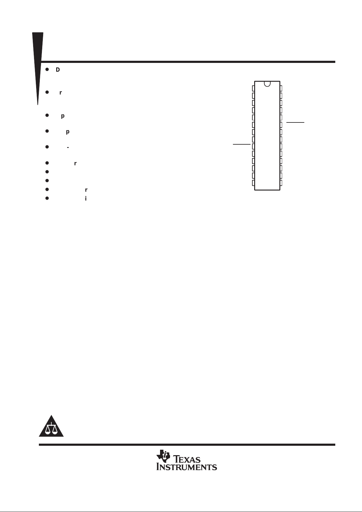
1HF
1AF/AE
1WRTCLK
1WRTEN
1IR
1D
GND
GND
1RESET
2Q
2OR
2RDEN
2RDCLK
2OE
1OE
1RDCLK
1RDEN
1OR
1Q
2RESET
V
CC
V
CC
2D
2IR
2WRTEN
2WRTCLK
2AF/AE
2HF
DW PACKAGE
(TOP VIEW)
SN74ACT2227, SN74ACT2229
DUAL 64 × 1, DUAL 256 × 1
FIRST-IN, FIRST-OUT MEMORIES
SCAS220C – JUNE 1992 – REVISED OCTOBER 1997
2
POST OFFICE BOX 655303 • DALLAS, TEXAS 75265
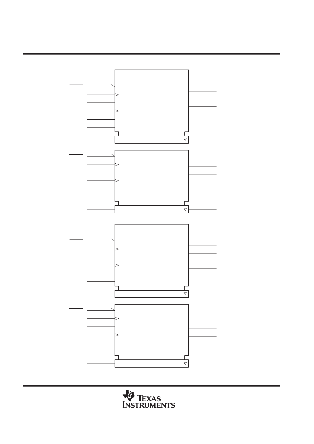
logic symbols
†
RESET
9
6
1D
1Q
24
Φ
FIFO 64 × 1
SN74ACT2227
3
1WRTCLK
WRTEN
4
1WRTEN
WRTCLK
27
1RDCLK
RDCLK
EN1
28
1OE
1IR
5
IN RDY
1HF
1
HALF FULL
1AF/AE
2
ALMOST FULL/EMPTY
1OR
25
OUT RDY
1RESET
1
RDEN
26
1RDEN
RESET
23
20
2D
2Q
10
17
2WRTCLK
WRTEN
18
2WRTEN
13
2RDCLK
EN2
14
2OE
2IR
19
2HF
15
2AF/AE
16
2OR
11
RDEN
12
2RDEN
2RESET
RESET
9
6
1D
1Q
24
Φ
FIFO 256 × 1
SN74ACT2229
3
1WRTCLK
WRTEN
4
1WRTEN
WRTCLK
27
1RDCLK
RDCLK
EN1
28
1OE
1IR
5
IN RDY
1HF
1
HALF FULL
1AF/AE
2
ALMOST FULL/EMPTY
1OR
25
OUT RDY
1RESET
1
RDEN
26
1RDEN
RESET
23
20
2D
2Q
10
17
2WRTCLK
WRTEN
18
2WRTEN
13
2RDCLK
EN2
14
2OE
2IR
19
2HF
15
2AF/AE
16
2OR
11
RDEN
12
2RDEN
2RESET
WRTCLK
RDCLK
WRTCLK
RDCLK
IN RDY
HALF FULL
ALMOST FULL/EMPTY
OUT RDY
2
IN RDY
HALF FULL
ALMOST FULL/EMPTY
OUT RDY
2
†
These symbols are in accordance with ANSI/IEEE Std 91-1984 and IEC Publication 617-12.
SN74ACT2227, SN74ACT2229
DUAL 64 × 1, DUAL 256 × 1
FIRST-IN, FIRST-OUT MEMORIES
SCAS220C – JUNE 1992 – REVISED OCTOBER 1997
3
POST OFFICE BOX 655303 • DALLAS, TEXAS 75265
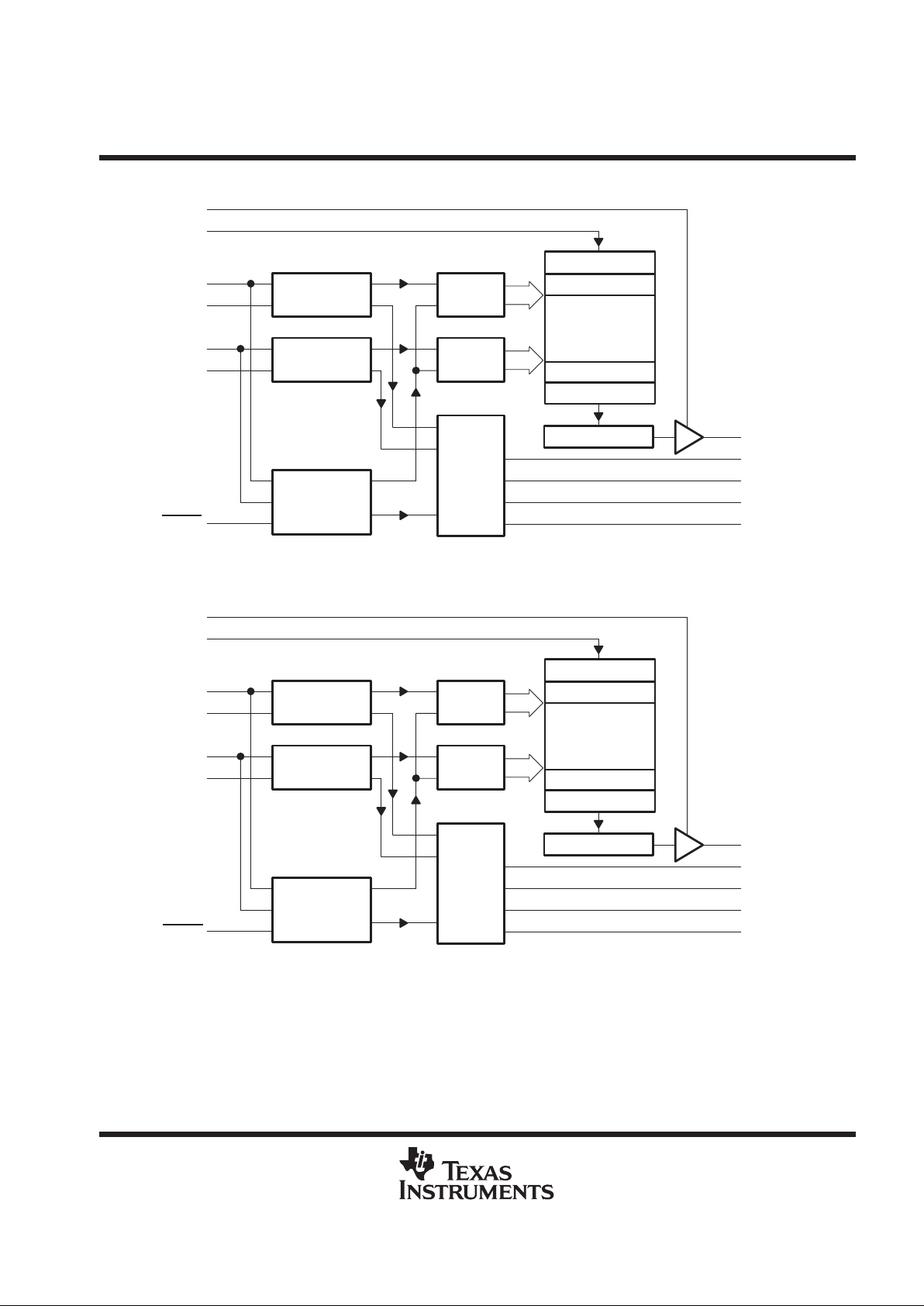
SN74ACT2227 functional block diagram (each FIFO)
Synchronous
Read Control
Read
Pointer
Location 1
Location 2
Dual-Port
SRAM
64 × 1
Location 63
Location 64
Synchronous
Write Control
Write
Pointer
Status
Register
D
RDCLK
RDEN
WRTCLK
WRTEN
RESET
Q
AF/AE
HF
IR
OR
Reset Logic
OE
SN74ACT2229 functional block diagram (each FIFO)
Synchronous
Read Control
Read
Pointer
Location 1
Location 2
Dual-Port
SRAM
256 × 1
Location 255
Location 256
Synchronous
Write Control
Write
Pointer
Status
Register
D
RDCLK
RDEN
WRTCLK
WRTEN
RESET
Q
AF/AE
HF
IR
OR
Reset Logic
OE
SN74ACT2227, SN74ACT2229
DUAL 64 × 1, DUAL 256 × 1
FIRST-IN, FIRST-OUT MEMORIES
SCAS220C – JUNE 1992 – REVISED OCTOBER 1997
4
POST OFFICE BOX 655303 • DALLAS, TEXAS 75265
Terminal Functions
TERMINAL
NAME NO.
I/O
DESCRIPTION
1AF/AE
2AF/AE
2
16
O
Almost-full/almost-empty flag. AF/AE is high when the memory is eight locations or fewer from a full or empty
state. AF/AE is set high after reset.
1D
2D
6
20
I Data input
GND 7, 8 Ground
1HF
2HF
1
15
O
Half-full flag. HF is high when the number of bits stored in memory is greater than or equal to half the FIFO depth.
HF is set low after reset.
1IR
2IR
5
19
O
Input-ready flag. IR is synchronized to the low-to-high transition of WRTCLK. When IR is low , the FIFO is full
and writes are disabled. IR is set low during reset and is set high on the second low-to-high transition of
WRTCLK after reset.
1OE
2OE
28
14
I
Output enable. The data output of a FIFO is active when OE is high and in the high-impedance state when OE
is low.
1OR
2OR
25
11
O
Output-ready flag. OR is synchronized to the low-to-high transition of RDCLK. When OR is low, the FIFO is
empty and reads are disabled. Ready data is present on the data output when OR is high. OR is set low during
reset and set high on the third low-to-high transition of RDCLK after the first word is loaded to empty memory.
1Q
2Q
24
10
O
Data outputs. After the first valid write to empty memory, the first bit is output on the third rising edge of RDCLK.
OR for the FIFO is asserted high to indicate ready data.
1RDCLK
2RDCLK
27
13
I
Read clock. RDCLK is a continuous clock and can be independent of any other clock on the device. A
low-to-high transition of RDCLK reads data from memory when the FIFO RDEN and OR are high. OR is
synchronous with the low-to-high transition of RDCLK.
1RDEN
2RDEN
26
12
I
Read enable. When the RDEN and OR of a FIFO are high, data is read from the FIFO on the low-to-high
transition of RDCLK.
1RESET
2RESET
9
23
I
Reset. To reset the FIFO, four low-to-high transitions of RDCLK and four low-to-high transitions of WRTCLK
must occur while RESET
is low. This sets HF, IR, and OR low and AF/AE high. Before it is used, a FIFO must
be reset after power up.
V
CC
21, 22 Supply voltage
1WRTCLK
2WRTCLK
3
17
I
Write clock. WRTCLK is a continuous clock and can be independent of any other clock on the device. A
low-to-high transition of WRTCLK writes data to memory when WRTEN and IR are high. IR is synchronous with
the low-to-high transition of WRTCLK.
1WRTEN
2WRTEN
4
18
I Write enable. When WRTEN and IR are high, data is written to the FIFO on a low-to-high transition of WRTCLK.

SN74ACT2227, SN74ACT2229
DUAL 64 × 1, DUAL 256 × 1
FIRST-IN, FIRST-OUT MEMORIES
SCAS220C – JUNE 1992 – REVISED OCTOBER 1997
5
POST OFFICE BOX 655303 • DALLAS, TEXAS 75265
IR
HF
AF/AE
OR
Q
RDEN
RDCLK
D
WRTEN
WRTCLK
RESET
4321
214321
Don’t Care
Don’t Care
Don’t Care
Don’t Care
Don’t Care
Don’t Care
Don’t Care
OE Don’t Care
Figure 1. FIFO Reset

SN74ACT2227, SN74ACT2229
DUAL 64 × 1, DUAL 256 × 1
FIRST-IN, FIRST-OUT MEMORIES
SCAS220C – JUNE 1992 – REVISED OCTOBER 1997
6
POST OFFICE BOX 655303 • DALLAS, TEXAS 75265
B1
CBAB10B4B3B2B1
IR
HF
AF/AE
OR
Q
RDEN
RDCLK
D
WRTEN
WRTCLK
RESET
1
0
1
0
1
0
OE
1
0
321
DATA BIT NUMBER BASED ON FIFO DEPTH
DATA BIT
DEVICE
A B C
SN74ACT2227 B33 B57 B65
SN74ACT2229 B129 B249 B257
Figure 2. FIFO Write

SN74ACT2227, SN74ACT2229
DUAL 64 × 1, DUAL 256 × 1
FIRST-IN, FIRST-OUT MEMORIES
SCAS220C – JUNE 1992 – REVISED OCTOBER 1997
7
POST OFFICE BOX 655303 • DALLAS, TEXAS 75265
D
IR
HF
AF/AE
OR
Q
RDEN
RDCLK
WRTEN
WRTCLK
RESET
FEDCBAB10B9B3B2B1
21
F
1
0
1
0
OE
DATA BIT NUMBER BASED ON FIFO DEPTH
DATA BIT
DEVICE
A B C D E F
SN74ACT2227 B33 B34 B56 B57 B64 B65
SN74ACT2229 B129 B130 B248 B249 B256 B257
Figure 3. FIFO Read

SN74ACT2227, SN74ACT2229
DUAL 64 × 1, DUAL 256 × 1
FIRST-IN, FIRST-OUT MEMORIES
SCAS220C – JUNE 1992 – REVISED OCTOBER 1997
8
POST OFFICE BOX 655303 • DALLAS, TEXAS 75265
absolute maximum ratings over operating free-air temperature range (unless otherwise noted)
†
Supply voltage range, V
CC
–0.5 V to 7 V. . . . . . . . . . . . . . . . . . . . . . . . . . . . . . . . . . . . . . . . . . . . . . . . . . . . . . . . . .
Input voltage range, V
I
(see Note 1) –0.5 V to VCC + 0.5 V. . . . . . . . . . . . . . . . . . . . . . . . . . . . . . . . . . . . . . . . . .
Output voltage range, V
O
(see Note 1) –0.5 V to VCC + 0.5 V. . . . . . . . . . . . . . . . . . . . . . . . . . . . . . . . . . . . . . .
Voltage applied to a disabled 3-state output 5.5 V. . . . . . . . . . . . . . . . . . . . . . . . . . . . . . . . . . . . . . . . . . . . . . . . . .
Input clamp current, I
IK
(VI < 0 or VI > VCC) ±20 mA. . . . . . . . . . . . . . . . . . . . . . . . . . . . . . . . . . . . . . . . . . . . . . . .
Output clamp current, I
OK
(VO < 0 or VO > VCC) ±50 mA. . . . . . . . . . . . . . . . . . . . . . . . . . . . . . . . . . . . . . . . . . . .
Continuous output current, I
O
(VO = 0 to VCC) ±50 mA. . . . . . . . . . . . . . . . . . . . . . . . . . . . . . . . . . . . . . . . . . . . . .
Continuous current through V
CC
or GND ±200 mA. . . . . . . . . . . . . . . . . . . . . . . . . . . . . . . . . . . . . . . . . . . . . . . . . .
Package thermal impedance, θ
JA
(see Note 2) 78°C/W. . . . . . . . . . . . . . . . . . . . . . . . . . . . . . . . . . . . . . . . . . . . . .
Storage temperature range, T
stg
–65°C to 150°C. . . . . . . . . . . . . . . . . . . . . . . . . . . . . . . . . . . . . . . . . . . . . . . . . . .
†
Stresses beyond those listed under “absolute maximum ratings” may cause permanent damage to the device. These are stress ratings only, and
functional operation of the device at these or any other conditions beyond those indicated under “recommended operating conditions” is not
implied. Exposure to absolute-maximum-rated conditions for extended periods may affect device reliability.
NOTES: 1. The input and output voltage ratings may be exceeded provided that the input and output current ratings are observed.
2. The package thermal impedance is calculated in accordance with JESD 51.
recommended operating conditions
MIN MAX UNIT
V
CC
Supply voltage 4.5 5.5 V
V
IH
High-level input voltage 2 V
V
IL
Low-level input voltage 0.8 V
I
OH
High-level output current Q outputs, flags –8 mA
p
Q outputs 16
IOLLow-level output current
Flags 8
mA
T
A
Operating free-air temperature –40 85 °C
electrical characteristics over recommended operating free-air temperature range (unless
otherwise noted)
PARAMETER TEST CONDITIONS MIN TYP‡MAX UNIT
V
OH
VCC = 4.5 V, IOH = – 8 mA 2.4 V
Flags VCC = 4.5 V, IOL = 8 mA 0.5
V
OL
Q outputs VCC = 4.5 V, IOL = 16 mA 0.5
V
I
I
VCC = 5.5 V, VI = VCC or 0 ±5 µA
I
OZ
VCC = 5.5 V, VO = VCC or 0 ±5 µA
I
CC
VI = VCC – 0.2 V or 0 400 µA
∆I
CC
§
VCC = 5.5 V, One input at 3.4 V , Other inputs at VCC or GND 1 mA
C
i
VI = 0, f = 1 MHz 4 pF
C
o
VO = 0, f = 1 MHz 8 pF
‡
All typical values are at VCC = 5 V, TA = 25°C.
§
This is the supply current when each input is at one of the specified TTL voltage levels rather than 0 V or VCC.

SN74ACT2227, SN74ACT2229
DUAL 64 × 1, DUAL 256 × 1
FIRST-IN, FIRST-OUT MEMORIES
SCAS220C – JUNE 1992 – REVISED OCTOBER 1997
9
POST OFFICE BOX 655303 • DALLAS, TEXAS 75265
timing requirements over recommended ranges of supply voltage and operating free-air
temperature (unless otherwise noted) (see Figures 1 through 4)
MIN MAX UNIT
f
clock
Clock frequency 60 MHz
1WRTCLK, 2WRTCLK high or low 5
twPulse duration
1RDCLK, 2RDCLK high or low 5
ns
1D before 1WRTCLK↑ and 2D before 2WRTCLK↑ 4.5
1WRTEN before 1WRTCLK↑and 2WRTEN before 2WRTCLK↑ 4.5
t
su
Setup time
1RDEN before 1RDCLK↑ and 2RDEN before 2RDCLK↑ 4
ns
1RESET low before 1WRTCLK↑ and 2RESET low before 2WRTCLK↑
†
6
1RESET low before 1RDCLK↑ and 2RESET low before 2RDCLK↑
†
6
1D after 1WRTCLK↑ and 2D after 2WRTCLK↑ 0
1WRTEN after 1WRTCLK↑and 2WRTEN after 2WRTCLK↑ 0
t
h
Hold time
1RDEN after 1RDCLK↑ and 2RDEN after 2RDCLK↑ 0
ns
1RESET low after 1WRTCLK↑ and 2RESET low after 2WRTCLK↑
†
6
1RESET low after 1RDCLK↑ and 2RESET low after 2RDCLK↑
†
6
†
Requirement to count the clock edge as one of at least four needed to reset a FIFO
switching characteristics over recommended ranges of supply voltage and operating free-air
temperature, C
L
= 50 pF (unless otherwise noted) (see Figure 4)
PARAMETER
FROM
(INPUT)
TO
(OUTPUT)
MIN MAX UNIT
f
max
1WRTCLK, 2WRTCLK,
or 1RDCLK, 2RDCLK
60 MHz
t
pd
1RDCLK↑, 2RDCLK↑ 1Q, 2Q 2 9 ns
t
pd
1WRTCLK↑, 2WRTCLK↑ 1IR, 2IR 1 8 ns
t
pd
1RDCLK↑, 2RDCLK↑ 1OR, 2OR 1 8 ns
1WRTCLK↑, 2WRTCLK↑
3 14
t
pd
1RDCLK↑, 2RDCLK↑
1AF/AE, 2AF/AE
3 14
ns
t
PLH
1WRTCLK↑, 2WRTCLK↑
2 12 ns
t
PHL
1RDCLK↑, 2RDCLK↑
1HF, 2HF
3 14 ns
t
PLH
1AF/AE, 2AF/AE 1 17 ns
t
PHL
1RESET, 2RESET l
ow
1HF, 2HF 1 18 ns
t
en
1OE, 2OE 1Q, 2Q 0 8 ns
t
dis
1OE, 2OE 1Q, 2Q 0 8 ns

SN74ACT2227, SN74ACT2229
DUAL 64 × 1, DUAL 256 × 1
FIRST-IN, FIRST-OUT MEMORIES
SCAS220C – JUNE 1992 – REVISED OCTOBER 1997
10
POST OFFICE BOX 655303 • DALLAS, TEXAS 75265
PARAMETER MEASUREMENT INFORMATION
V
OH
V
OL
t
h
t
PLH
t
PHL
Output
Control
Output
Waveform 1
S1 at 7 V
Output
Waveform 2
S1 at Open
t
PZL
t
PZH
t
PLZ
t
PHZ
1.5 V1.5 V
1.5 V 1.5 V
3 V
0 V
1.5 V 1.5 V
V
OH
V
OL
0 V
1.5 V
VOL + 0.3 V
1.5 V
VOH – 0.3 V
≈ 0 V
1.5 V
3 V
0 V
1.5 V 1.5 V
0 V
3 V
0 V
1.5 V 1.5 V
t
w
Input
3 V
3 V
≈ 3.5 V
VOLTAGE WAVEFORMS
SETUP AND HOLD TIMES
VOLTAGE WAVEFORMS
PROPAGATION DELAY TIMES
VOLTAGE WAVEFORMS
PULSE DURATION
VOLTAGE WAVEFORMS
ENABLE AND DISABLE TIMES
Timing
Input
Data
Input
Output
Input
S1
500 Ω
LOAD CIRCUIT
500 Ω
7 V
From Output
Under Test
Test
Point
CL = 50 pF
(see Note A)
t
su
t
PZH
t
PZL
t
PHZ
t
PLZ
t
PLH
t
PHL
Open
Closed
Open
Closed
Open
Open
PARAMETER S1
t
en
t
dis
t
pd
NOTE A: CL includes probe and jig capacitance.
Figure 4. Load Circuit and Voltage Waveforms

SN74ACT2227, SN74ACT2229
DUAL 64 × 1, DUAL 256 × 1
FIRST-IN, FIRST-OUT MEMORIES
SCAS220C – JUNE 1992 – REVISED OCTOBER 1997
11
POST OFFICE BOX 655303 • DALLAS, TEXAS 75265
TYPICAL CHARACTERISTICS
0
5
10
15
20
25
30
35
40
0 102030405060
I – Supply Current – mA
CC(f)
SINGLE FIFO SUPPLY CURRENT
vs
CLOCK FREQUENCY
f
clock
– Clock Frequency – MHz
fI = 1/2 f
clock
TA = 75°C
CL = 0 pF
VCC = 5.5 V
VCC = 5 V
VCC = 4.5 V
Figure 5
calculating power dissipation
Data for Figure 5 is taken with one FIFO active and one FIFO idle on the device. The active FIFO has both writes
and reads enabled with its read clock (RDCLK) and write clock (WRTCLK) operating at the rate specified by
f
clock
. The data input rate and data output rate are half the f
clock
rate, and the data output is disconnected. A
close approximation to the total device power can be found by Figure 5, determining the capacitive load on the
data output and determining the number of SN74ACT2227/2229 inputs driven by TTL high levels.
With I
CC(f)
taken from Figure 5, the maximum power dissipation (PT) of one FIFO on the SN74ACT2227 or
SN74ACT2229 can be calculated by:
P
T
= VCC × [I
CC(f)
+ (N × ∆ICC × dc)] + (CL × V
CC
2
× fo)
where:
N = number of inputs driven by TTL levels
∆I
CC
= increase in power-supply current for each input at a TTL high level
dc = duty cycle of inputs at a TTL high level of 3.4 V
C
L
= output capacitive load
f
o
= switching frequency of an output

SN74ACT2227, SN74ACT2229
DUAL 64 × 1, DUAL 256 × 1
FIRST-IN, FIRST-OUT MEMORIES
SCAS220C – JUNE 1992 – REVISED OCTOBER 1997
12
POST OFFICE BOX 655303 • DALLAS, TEXAS 75265
APPLICATION INFORMATION
An example of concentrating two independent serial-data signals into a single composite data signal with the use of
an SN74ACT2227 or SN74ACT2229 device is shown in Figure 6. The input data to the FIFOs share the same average
(mean) frequency and the mean frequency of the SYS_CLOCK is greater than or equal to the sum of the individual
mean input rates. A single-bit FIFO is needed for each additional input data signal that is time-division multiplexed
into the composite signal.
The FIFO memories provide a buffer to absorb clock jitter generated by the transmission systems of incoming signals
and synchronize the phase-independent inputs to one another. FIFO half-full (HF) flags are used to signal the
multiplexer to start fetching data from the buffers. The state of the flags also can be used to indicate when a FIFO
read should be suppressed to regulate the output flow (pulse-stuffing control). The FIFO almost-full/almost-empty
(AF/AE) flags can be used in place of the half-full flags to reduce transmission delay.
1HF
1WRTCLK
1WRTEN
1D
1RDCLK
1RDEN
1Q
2HF
2D
2WRTEN
2WRTCLK
2Q
2RDEN
2RDCLK
READY_1
SELECT_1
DATA_1
SELECT_2
DATA_2
READY_2
SN74ACT2227
or
SN74ACT2229
Serial
Data
Stream
Serial
Data
Stream
+5 V
Time-Division
Multiplexer
SYS_CLOCK
Composite
Data Stream
Figure 6. Time-Division Multiplexing Using the SN74ACT2227 or SN74ACT2229

IMPORTANT NOTICE
T exas Instruments and its subsidiaries (TI) reserve the right to make changes to their products or to discontinue
any product or service without notice, and advise customers to obtain the latest version of relevant information
to verify, before placing orders, that information being relied on is current and complete. All products are sold
subject to the terms and conditions of sale supplied at the time of order acknowledgement, including those
pertaining to warranty, patent infringement, and limitation of liability.
TI warrants performance of its semiconductor products to the specifications applicable at the time of sale in
accordance with TI’s standard warranty. Testing and other quality control techniques are utilized to the extent
TI deems necessary to support this warranty. Specific testing of all parameters of each device is not necessarily
performed, except those mandated by government requirements.
CERT AIN APPLICATIONS USING SEMICONDUCTOR PRODUCTS MA Y INVOLVE POTENTIAL RISKS OF
DEATH, PERSONAL INJURY, OR SEVERE PROPERTY OR ENVIRONMENTAL DAMAGE (“CRITICAL
APPLICATIONS”). TI SEMICONDUCTOR PRODUCTS ARE NOT DESIGNED, AUTHORIZED, OR
WARRANTED TO BE SUITABLE FOR USE IN LIFE-SUPPORT DEVICES OR SYSTEMS OR OTHER
CRITICAL APPLICATIONS. INCLUSION OF TI PRODUCTS IN SUCH APPLICA TIONS IS UNDERST OOD TO
BE FULLY AT THE CUSTOMER’S RISK.
In order to minimize risks associated with the customer’s applications, adequate design and operating
safeguards must be provided by the customer to minimize inherent or procedural hazards.
TI assumes no liability for applications assistance or customer product design. TI does not warrant or represent
that any license, either express or implied, is granted under any patent right, copyright, mask work right, or other
intellectual property right of TI covering or relating to any combination, machine, or process in which such
semiconductor products or services might be or are used. TI’s publication of information regarding any third
party’s products or services does not constitute TI’s approval, warranty or endorsement thereof.
Copyright 1999, Texas Instruments Incorporated
 Loading...