

D
Members of the Texas Instruments
Widebus+
D
State-of-the-Art
Family
EPIC-ΙΙB
BiCMOS Design
Significantly Reduces Power Dissipation
D
UBE
(Universal Bus Exchanger)
Combines D-Type Latches and D-Type
Flip-Flops for Operation in Transparent,
Latched, Clocked, or Clock-Enabled Mode
D
ESD Protection Exceeds 2000 V Per
MIL-STD-883, Method 3015
D
Latch-Up Performance Exceeds 500 mA
Per JEDEC Standard JESD-17
D
Typical V
(Output Ground Bounce)
OLP
< 0.8 V at VCC = 5 V, TA = 25°C
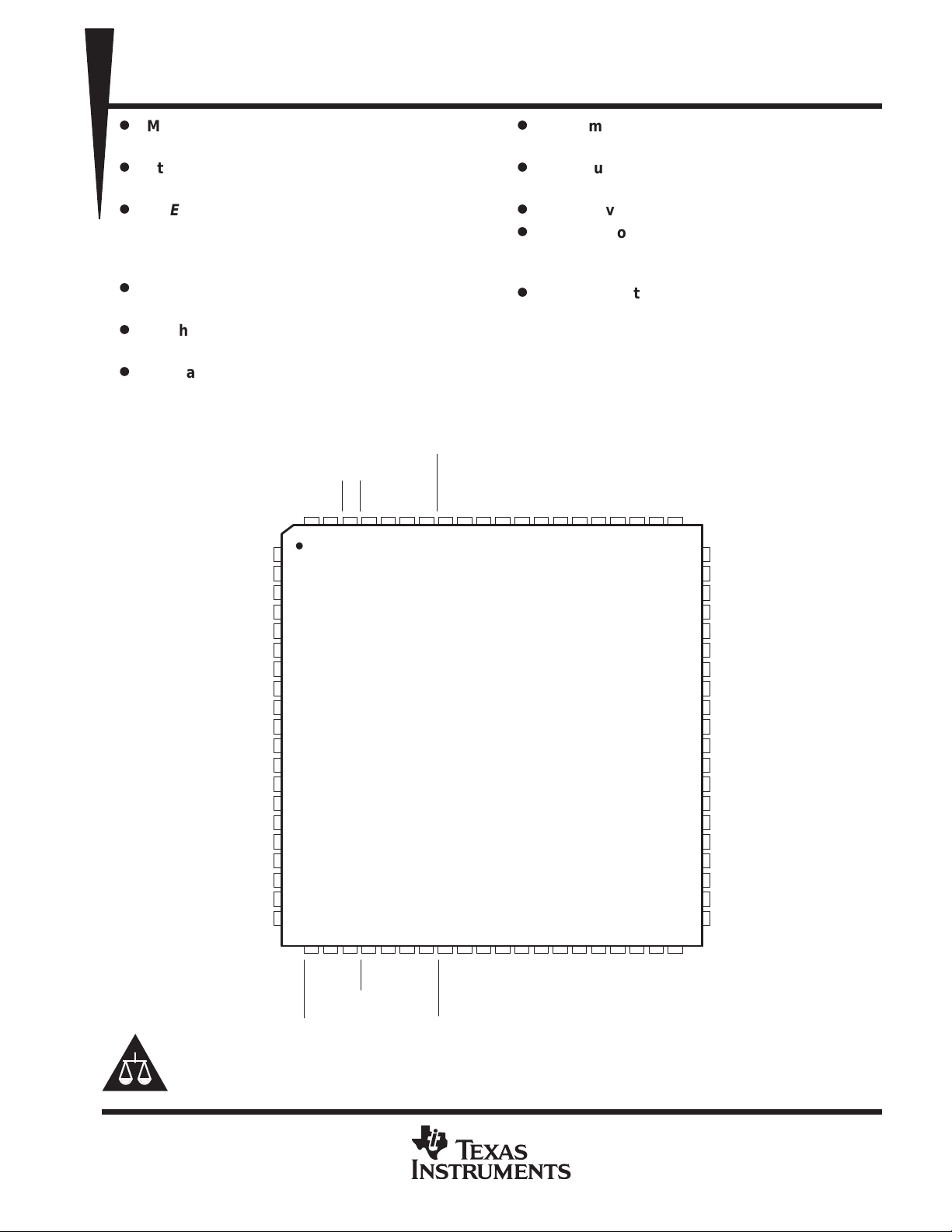
SN54ABTH32316, SN74ABTH32316
16-BIT TRI-PORT UNIVERSAL BUS EXCHANGERS
SCBS179E – JUNE 1992 – REVISED MA Y 1997
D
High-Impedance State During Power Up
and Power Down
D
Distributed VCC and GND Pin Configuration
Minimizes High-Speed Switching Noise
D
High-Drive Outputs (–32-mA IOH, 64-mA IOL)
D
Bus Hold on Data Inputs Eliminates the
Need for External Pullup/Pulldown
Resistors
D
Package Options Include 80-Pin Plastic
Thin Quad Flat (PN) Package With
12 × 12-mm Body Using 0.5-mm Lead Pitch
and 84-Pin Ceramic Quad Flat (HT) Package
A2
A3
A4
GND
A5
A6
A7
A8
A9
V
CC
GND
A10
A11
A12
A13
A14
GND
A15
A16
NC
A1
SELA
79 78 77 76 7580 74
1
2
3
4
5
6
7
8
9
10
11
12
13
14
15
16
17
18
19
20
22 23
21
OEA
OEC
25 26 27 28
24
’ABTH32316 . . . PN PACKAGE
SELC
LEC
(TOP VIEW)
CLKC
CLKENC
NC
72 71 7073
29 30 31 32 33
GND
VCCC16
69 68
C15
C14
C13
67 66 65 64
34 35 36 37
C12
C1 1
GND
63 62 61
38 39 40
C10
C9
60
59
58
57
56
55
54
53
52
51
50
49
48
47
46
45
44
43
42
41
C8
C7
C6
GND
C5
C4
C3
C2
C1
V
CC
GND
B16
B15
B14
B13
B12
GND
B11
B10
B9
B1
CC
LEA
CLKA
CLKENA
NC – No internal connection
Please be aware that an important notice concerning availability, standard warranty, and use in critical applications of
Texas Instruments semiconductor products and disclaimers thereto appears at the end of this data sheet.
Widebus+, EPIC-ΙΙB, and UBE are trademarks of Texas Instruments Incorporated.
PRODUCTION DATA information is current as of publication date.
Products conform to specifications per the terms of Texas Instruments
standard warranty. Production processing does not necessarily include
testing of all parameters.
LEB
OEB
SELB
POST OFFICE BOX 655303 • DALLAS, TEXAS 75265
CLKB
CLKENB
NC
V
GND
B2
B3B4B5
B6
B7
GND
B8
Copyright 1997, Texas Instruments Incorporated
1
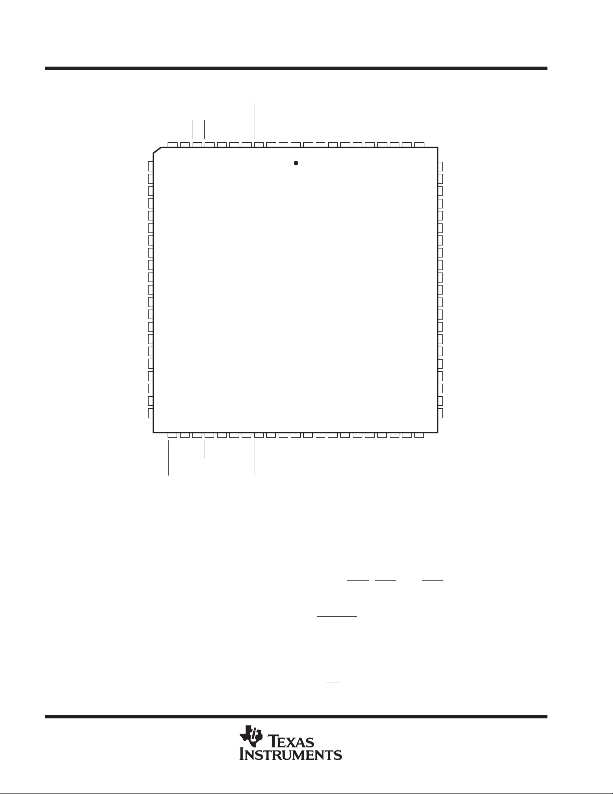
SN54ABTH32316, SN74ABTH32316
16-BIT TRI-PORT UNIVERSAL BUS EXCHANGERS
SCBS179E – JUNE 1992 – REVISED MA Y 1997
A2
A3
A4
GND
A5
A6
A7
A8
A9
V
CC
NC
GND
A10
A11
A12
A13
A14
GND
A15
A16
NC
A1
SELA
83 82 81 80 7984 78
1
2
3
4
5
6
7
8
9
10
11
12
13
14
15
16
17
18
19
20
21
23 24
22
SN54ABTH32316 ...HT PACKAGE
OEA
OEC
SELC
LEC
26 27 28 29
25
(TOP VIEW)
CLKC
NC
CLKENC
76 75 7477
30 31 32 33 34
VCCGND
NC
73 72
C15
C14
C16
71 70 69 68
35 36 37 38
C13
C12
GND
C11
C10
67 66 65 64
39 40 41 42
C9
63
62
61
60
59
58
57
56
55
54
53
52
51
50
49
48
47
46
45
44
43
C8
C7
C6
GND
C5
C4
C3
C2
C1
V
CC
NC
GND
B16
B15
B14
B13
B12
GND
B11
B10
B9
B6
LEA
OEB
CLKA
CLKENA
NC – No internal connection
LEB
SELB
CLKB
CLKENB
NC
V
CC
NC
GND
B2B3B4
B1
B5
GND
B7
B8
description
The ’ABTH32316 consist of three 16-bit registered input/output (I/O) ports. These registers combine D-type
latches and flip-flops to allow data flow in transparent, latch, and clock modes. Data from one input port can be
exchanged to one or more of the other ports. Because of the universal storage element, multiple combinations
of real-time and stored data can be exchanged among the three ports.
Data flow in each direction is controlled by the output-enable (OEA
SELB, and SELC), latch-enable (LEA, LEB, and LEC), and clock (CLKA, CLKB, and CLKC) inputs. The A data
register operates in the transparent mode when LEA is high. When LEA is low, data is latched if CLKA is held
at a high or low logic level. If LEA and clock-enable A (CLKENA) are low, data is stored on the low-to-high
transition of CLKA. Output data selection is accomplished by the select-control pins. All three ports have
active-low output enables, so when the output-enable input is low, the outputs are active; when the
output-enable input is high, the outputs are in the high-impedance state.
When VCC is between 0 and 2.1 V , the device is in the high-impedance state during power up or power down.
However, to ensure the high-impedance state above 2.1 V, OE
the minimum value of the resistor is determined by the current-sinking capability of the driver.
, OEB, and OEC), select-control (SELA,
should be tied to VCC through a pullup resistor;
2
POST OFFICE BOX 655303 • DALLAS, TEXAS 75265
OUTPUT
OUTPUT A
OUTPUT B
OUTPUT C
SN54ABTH32316, SN74ABTH32316
16-BIT TRI-PORT UNIVERSAL BUS EXCHANGERS
SCBS179E – JUNE 1992 – REVISED MA Y 1997
description (continued)
Active bus-hold circuitry is provided to hold unused or floating data inputs at a valid logic level.
The SN54ABTH32316 is characterized for operation over the full military temperature range of –55°C to 125°C.
The SN74ABTH32316 is characterized for operation from –40°C to 85°C.
Function Tables
STORAGE
INPUTS
CLKENA CLKA LEA A
H X L X Q
L ↑ LL L
L ↑ LH H
X HLXQ
X LLXQ
X XHL L
X X H H H
†
A-port register shown. B and C ports are similar
but use CLKENB
and LEC.
‡
Output level before the indicated steady-state
input conditions were established
INPUTS
OEA SELA
H X Z
L H Output of C register
L L Output of B register
, CLKENC, CLKB, CLKC, LEB,
A-PORT OUTPUT
†
0
0
0
‡
‡
‡
B-PORT OUTPUT
INPUTS
OEB SELB
H X Z
L H Output of A register
L L Output of C register
C-PORT OUTPUT
INPUTS
OEC SELC
H X Z
L H Output of B register
L L Output of A register
POST OFFICE BOX 655303 • DALLAS, TEXAS 75265
3

SN54ABTH32316, SN74ABTH32316
16-BIT TRI-PORT UNIVERSAL BUS EXCHANGERS
SCBS179E – JUNE 1992 – REVISED MA Y 1997
logic diagram (positive logic)
77
OEC
LEC
C1
OEB
LEB
76
74
73
75
52
24
25
27
28
26
C
CE
C
CE
SELC
CLKC
CLKENC
SELB
CLKB
CLKENB
CLK
CLK
32
B1
78
OEA
LEA
A1
79
22
21
23
80
SELA
CLKA
CLKENA
Pin numbers shown are for the PN package.
CLK
C
CE
1 of 16 Channels
4
POST OFFICE BOX 655303 • DALLAS, TEXAS 75265

UNIT
SN54ABTH32316, SN74ABTH32316
16-BIT TRI-PORT UNIVERSAL BUS EXCHANGERS
SCBS179E – JUNE 1992 – REVISED MA Y 1997
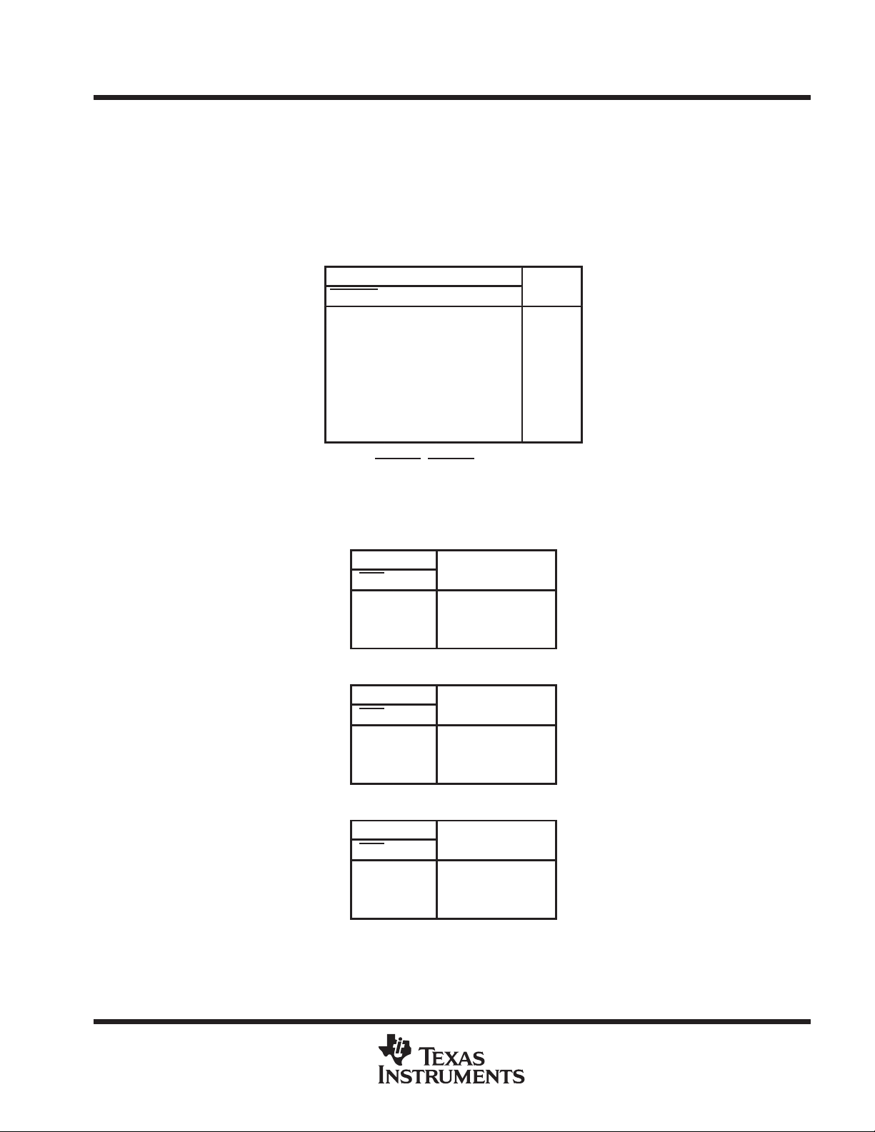
absolute maximum ratings over operating free-air temperature range (unless otherwise noted)
Supply voltage range, V
Input voltage range, VI (except I/O ports) (see Note 1) –0.5 V to 7 V. . . . . . . . . . . . . . . . . . . . . . . . . . . . . . . . . .
Voltage range applied to any output in the high or power-off state, VO –0.5 V to 5.5 V. . . . . . . . . . . . . . . . . . .
Current into any output in the low state, IO: SN54ABTH32316 96 mA. . . . . . . . . . . . . . . . . . . . . . . . . . . . . . . . .
Input clamp current, I
Output clamp current, I
Package thermal impedance, θJA (see Note 2): PN package 62°C/W. . . . . . . . . . . . . . . . . . . . . . . . . . . . . . . . . .
Storage temperature range, T
†
Stresses beyond those listed under “absolute maximum ratings” may cause permanent damage to the device. These are stress ratings only, and
functional operation of the device at these or any other conditions beyond those indicated under “recommended operating conditions” is not
implied. Exposure to absolute-maximum-rated conditions for extended periods may affect device reliability.
NOTES: 1. The input and output negative-voltage ratings may be exceeded if the input and output clamp-current ratings are observed.
2. The package thermal impedance is calculated in accordance with EIA/JEDEC Std JESD51.
–0.5 V to 7 V. . . . . . . . . . . . . . . . . . . . . . . . . . . . . . . . . . . . . . . . . . . . . . . . . . . . . . . . . .
CC
SN74ABTH32316 128 mA. . . . . . . . . . . . . . . . . . . . . . . . . . . . . . . .
(V
< 0) –18 mA. . . . . . . . . . . . . . . . . . . . . . . . . . . . . . . . . . . . . . . . . . . . . . . . . . . . . . . . . . .
IK
I
(V
OK
< 0) –50 mA. . . . . . . . . . . . . . . . . . . . . . . . . . . . . . . . . . . . . . . . . . . . . . . . . . . . . . . .
O
–65°C to 150°C. . . . . . . . . . . . . . . . . . . . . . . . . . . . . . . . . . . . . . . . . . . . . . . . . . .
stg
recommended operating conditions (see Note 3)
SN54ABTH32316 SN74ABTH32316
MIN MAX MIN MAX
V
CC
V
IH
V
IL
V
I
I
OH
I
OL
∆t/∆v Input transition rise or fall rate Outputs enabled 10 10 ns/V
∆t/∆V
T
A
NOTE 3: Unused control pins must be held high or low to prevent them from floating.
Supply voltage 4.5 5.5 4.5 5.5 V
High-level input voltage 2 2 V
Low-level input voltage 0.8 0.8 V
Input voltage 0 V
High-level output current –24 –32 mA
Low-level output current 48 64 mA
Power-up ramp rate 200 200 µs/V
CC
Operating free-air temperature –55 125 –40 85 °C
CC
0 V
CC
V
†
POST OFFICE BOX 655303 • DALLAS, TEXAS 75265
5

SN54ABTH32316, SN74ABTH32316
PARAMETER
TEST CONDITIONS
UNIT
V
V
V
4.5 V
VOLV
V
V
I
A
I
A, B, or C ports
V
V
A
V
CC
UNIT
twPulse duration
ns
16-BIT TRI-PORT UNIVERSAL BUS EXCHANGERS
SCBS179E – JUNE 1992 – REVISED MA Y 1997
electrical characteristics over recommended operating free-air temperature range (unless
otherwise noted)
SN54ABTH32316 SN74ABTH32316
MIN TYP†MAX MIN TYP†MAX
V
IK
OH
V
hys
I
I(hold)
I
OZPU
I
OZPD
I
off
I
CEX
I
O
I
CC
∆I
C
C
†
All typical values are at VCC = 5 V, TA = 25°C.
‡
This parameter is specified by characterization.
§
Not more than one output should be tested at a time, and the duration of the test should not exceed one second.
¶
This is the increase in supply current for each input that is at the specified TTL voltage level rather than VCC or GND.
Control inputs VCC = 0 to 5.5 V, VI = VCC or GND ±1 ±1
A, B, or C ports VCC = 2.1 V to 5.5 V, VI = VCC or GND ±100 ±20
p
‡
‡
§
¶
CC
Control inputs VI = 2.5 V or 0.5 V 3 3 pF
i
A, B, or C ports VO = 2.5 V or 0.5 V 11.5 1 1.5 pF
io
VCC = 4.5 V, II = –18 mA –1.2 –1.2 V
VCC = 4.5 V, IOH = –3 mA 2.5 2.5
VCC = 5 V, IOH = –3 mA 3 3
=
CC
= 4.5
CC
= 4.5
CC
VCC = 0 to 2.1 V, VO = 0.5 V to 2.7 V, OE = X ±50 ±50 µA
VCC = 2.1 V to 0, VO = 0.5 V to 2.7 V, OE = X ±50 ±50 µA
VCC = 0, VI or VO ≤ 4.5 V ±100 ±100 µA
VCC = 5.5 V, VO = 5.5 V Outputs high 50 50 µA
VCC = 5.5 V, VO = 2.5 V –50 –100 –180 –50 –100 –180 mA
=
= 5.5 V,
IO = 0,
VI = VCC or GND
VCC = 5.5 V, One input at 3.4 V,
Other inputs at VCC or GND
IOH = –24 mA 2
IOH = –32 mA 2
IOL = 48 mA 0.55
IOL = 64 mA 0.55
100 100 mV
VI = 0.8 V 100 100
VI = 2 V –100 –100
Outputs high 2 2
Outputs low 40 40
Outputs disabled 1 1
1 0.5 mA
µ
µ
mA
timing requirements over recommended ranges of supply voltage and operating free-air
temperature (unless otherwise noted) (see Figure 1)
6
f
clock
t
su
t
h
Clock frequency 0 150 0 150 MHz
Setup time
Hold time
LE high 3.3 3.3
CLK high or low 3.3 3.3
A, B, or C before CLK↑ 2.6 2.4
A or B before LE↓
CLKEN before CLK↑ 3.5 3.2
A, B, or C after CLK↑ 1.8 1.4
A or B after LE↓
CLKEN after CLK↑ 1.5 1.1
POST OFFICE BOX 655303 • DALLAS, TEXAS 75265
SN54ABTH32316 SN74ABTH32316
MIN MAX MIN MAX
2.5 2.1
2.4 2.1
ns
ns

PARAMETER
UNIT
A, B, or C
C, B, or A
ns
SEL
A, B, or C
ns
LE
A, B, or C
ns
CLK
A, B, or C
ns
OE
A, B, or C
ns
OE
A, B, or C
ns
SN54ABTH32316, SN74ABTH32316
16-BIT TRI-PORT UNIVERSAL BUS EXCHANGERS
SCBS179E – JUNE 1992 – REVISED MA Y 1997
switching characteristics over recommended ranges of supply voltage and operating free-air
temperature, C
f
max
t
PLH
t
PHL
t
PLH
t
PHL
t
PLH
t
PHL
t
PLH
t
PHL
t
PZH
t
PZL
t
PHZ
t
PLZ
= 50 pF (unless otherwise noted) (see Figure 1)
L
FROM TO
(INPUT) (OUTPUT)
SN54ABTH32316 SN74ABTH32316
MIN MAX MIN MAX
150 150 MHz
0.8 6.5 1.4 6.1
0.5 6.8 1.1 6.6
0.8 6.7 1.4 6.5
0.8 6.8 1.8 6.5
1.5 8 2.6 7.5
1.5 7.4 2.6 6.9
1.5 8 2.5 7.5
1.5 7.2 2.5 6.7
0.8 6.7 1.5 6.4
1.5 7.1 2.4 6.8
0.8 7.2 1.5 6
0.8 6.4 1.9 6.1
POST OFFICE BOX 655303 • DALLAS, TEXAS 75265
7

SN54ABTH32316, SN74ABTH32316
16-BIT TRI-PORT UNIVERSAL BUS EXCHANGERS
SCBS179E – JUNE 1992 – REVISED MA Y 1997
PARAMETER MEASUREMENT INFORMATION
500 Ω
t
w
1.5 V
500 Ω
1.5 V
1.5 V1.5 V
From Output
Under Test
CL = 50 pF
(see Note A)
LOAD CIRCUIT
Input
Input
Output
Output
INVERTING AND NONINVERTING OUTPUTS
NOTES: A. CL includes probe and jig capacitance.
B. Waveform 1 is for an output with internal conditions such that the output is low except when disabled by the output control.
Waveform 2 is for an output with internal conditions such that the output is high except when disabled by the output control.
C. All input pulses are supplied by generators having the following characteristics: PRR ≤ 10 MHz, ZO = 50 Ω, tr ≤ 2.5 ns, tf≤ 2.5 ns.
D. The outputs are measured one at a time with one transition per measurement.
1.5 V
VOLTAGE WAVEFORMS
PULSE DURATION
1.5 V 1.5 V
t
PLH
t
PHL
VOLTAGE WAVEFORMS
PROPAGATION DELAY TIMES
S1
t
PHL
1.5 V
t
PLH
3 V
0 V
V
V
V
V
7 V
OH
OL
OH
OL
Open
GND
3 V
0 V
Timing Input
Data Input
Output
Control
Output
Waveform 1
S1 at 7 V
(see Note B)
Output
Waveform 2
S1 at Open
(see Note B)
TEST S1
t
PLH/tPHL
t
PLZ/tPZL
t
PHZ/tPZH
t
su
1.5 V 1.5 V
VOLTAGE WAVEFORMS
SETUP AND HOLD TIMES
t
PZL
t
PLZ
1.5 V
t
t
PZH
VOLTAGE WAVEFORMS
ENABLE AND DISABLE TIMES
LOW- AND HIGH-LEVEL ENABLING
PHZ
1.5 V
Open
Open
1.5 V
t
7 V
h
1.5 V1.5 V
VOL + 0.3 V
VOH – 0.3 V
3 V
0 V
3 V
0 V
3 V
0 V
3.5 V
V
OL
V
OH
≈ 0 V
Figure 1. Load Circuit and Voltage Waveforms
8
POST OFFICE BOX 655303 • DALLAS, TEXAS 75265

IMPORTANT NOTICE
T exas Instruments and its subsidiaries (TI) reserve the right to make changes to their products or to discontinue
any product or service without notice, and advise customers to obtain the latest version of relevant information
to verify, before placing orders, that information being relied on is current and complete. All products are sold
subject to the terms and conditions of sale supplied at the time of order acknowledgement, including those
pertaining to warranty, patent infringement, and limitation of liability.
TI warrants performance of its semiconductor products to the specifications applicable at the time of sale in
accordance with TI’s standard warranty. Testing and other quality control techniques are utilized to the extent
TI deems necessary to support this warranty . Specific testing of all parameters of each device is not necessarily
performed, except those mandated by government requirements.
CERTAIN APPLICA TIONS USING SEMICONDUCT OR PRODUCTS MAY INVOLVE POTENTIAL RISKS OF
DEATH, PERSONAL INJURY, OR SEVERE PROPERTY OR ENVIRONMENTAL DAMAGE (“CRITICAL
APPLICATIONS”). TI SEMICONDUCTOR PRODUCTS ARE NOT DESIGNED, AUTHORIZED, OR
WARRANTED TO BE SUITABLE FOR USE IN LIFE-SUPPORT DEVICES OR SYSTEMS OR OTHER
CRITICAL APPLICA TIONS. INCLUSION OF TI PRODUCTS IN SUCH APPLICATIONS IS UNDERST OOD TO
BE FULLY AT THE CUSTOMER’S RISK.
In order to minimize risks associated with the customer’s applications, adequate design and operating
safeguards must be provided by the customer to minimize inherent or procedural hazards.
TI assumes no liability for applications assistance or customer product design. TI does not warrant or represent
that any license, either express or implied, is granted under any patent right, copyright, mask work right, or other
intellectual property right of TI covering or relating to any combination, machine, or process in which such
semiconductor products or services might be or are used. TI’s publication of information regarding any third
party’s products or services does not constitute TI’s approval, warranty or endorsement thereof.
Copyright 1998, Texas Instruments Incorporated
 Loading...