

Datasheet SN74ABT863DBLE, SN74ABT863DBR, SN74ABT863DW, SN74ABT863DWR, SN74ABT863NT Datasheet (Texas Instruments)

SN54ABT863, SN74ABT863
9-BIT BUS TRANSCEIVERS
WITH 3-STATE OUTPUTS
SCBS201E – FEBRUARY 1991 – REVISED JULY 1998
D
State-of-the-Art
EPIC-ΙΙB
BiCMOS Design
Significantly Reduces Power Dissipation
D
T ypical V
at V
D
High-Impedance State During Power Up
= 5 V, TA = 25°C
CC
(Output Ground Bounce) < 1 V
OLP
and Power Down
D
High-Drive Outputs (–32-mA IOH, 64-mA IOL)
D
Latch-Up Performance Exceeds 500 mA Per
JESD 17
D
ESD Protection Exceeds 2000 V Per
MIL-STD-883, Method 3015; Exceeds 200 V
Using Machine Model (C = 200 pF, R = 0)
D
Package Options Include Plastic
Small-Outline (DW), Shrink Small-Outline
(DB) Packages, and Thin Shrink
Small-Outline (PW), Ceramic Chip Carriers
(FK), Plastic (NT), and Ceramic (JT) DIPs
description
The ’ABT863 devices are 9-bit transceivers
designed for asynchronous communication
between data buses. The control-function
implementation allows for maximum flexibility in
timing.
These devices allow noninverted data
transmission from the A bus to the B bus or from
the B bus to the A bus, depending on the logic
levels at the output-enable (OEAB
inputs.
and OEBA)
SN74ABT863 . . . DB, DW, NT, OR PW PACKAGE
SN54ABT863 . . . JT PACKAGE
(TOP VIEW)
OEBA1
OEBA2
SN54ABT863 . . . FK PACKAGE
A3
A4
A5
NC
A6
A7
A8
1
24
A1
2
23
A2
3
22
A3
4
21
A4
5
20
A5
6
19
A6
7
18
A7
8
17
A8
9
16
10
A9
GND
(TOP VIEW)
A2A1OEBA1NCB1
426
3212827
5
6
7
8
9
10
11
12 13
15
11
14
12
13
CC
V
14 15 16 17 18
V
CC
B1
B2
B3
B4
B5
B6
B7
B8
B9
OEAB2
OEAB1
B2
25
24
21
22
21
20
19
B3
B4
B5
NC
B6
B7
B8
The outputs are in the high-impedance state
during power up and power down. The outputs
remain in the high-impedance state while the
device is powered down.
When V
is between 0 and 2.1 V, the device is
CC
NC – No internal connection
A9
GND
OEBA2
NC
OEAB1
OEAB2
B9
in the high-impedance state during power up or
power down. However, to ensure the
high-impedance state above 2.1 V , OE
tied to V
through a pullup resistor; the minimum
CC
should be
value of the resistor is determined by the
current-sinking capability of the driver.
The SN54ABT863 is characterized for operation over the full military temperature range of –55°C to 125°C.
The SN74ABT863 is characterized for operation from –40°C to 85°C.
Please be aware that an important notice concerning availability, standard warranty, and use in critical applications of
Texas Instruments semiconductor products and disclaimers thereto appears at the end of this data sheet.
EPIC-ΙΙB is a trademark of Texas Instruments Incorporated.
UNLESS OTHERWISE NOTED this document contains PRODUCTION
DATA information current as of publication date. Products conform to
specifications per the terms of Texas Instruments standard warranty.
Production processing does not necessarily include testing of all
parameters.
Copyright 1998, Texas Instruments Incorporated
POST OFFICE BOX 655303 • DALLAS, TEXAS 75265
1
SN54ABT863, SN74ABT863
OPERATION
A
to
B
B
to
A
Isolation
9-BIT BUS TRANSCEIVERS
WITH 3-STATE OUTPUTS
SCBS201E – FEBRUARY 1991 – REVISED JULY 1998
OEAB1 OEAB2 OEBA1 OEBA2
L L L L Latch A and B
L L H X
L LXH
HXLL
XHLL
HXHX
HXXH
XHXH
XHHX
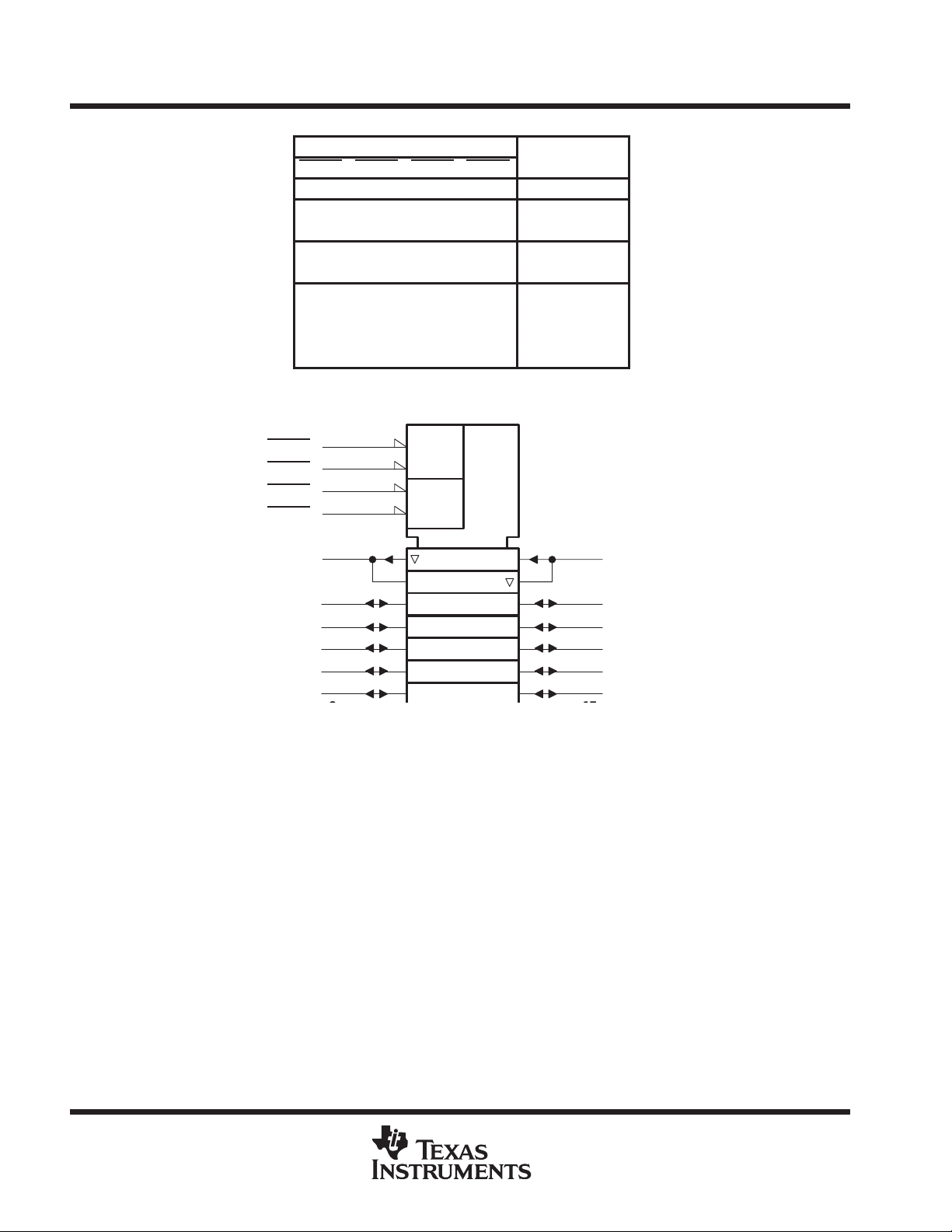
FUNCTION TABLE
INPUTS
logic symbol
†
OEBA1
OEBA2
OEAB1
OEAB2
A1
A2
A3
A4
A5
A6
1
11
13
14
2
3
4
5
6
7
&
&
121
1
EN1
EN2
23
22
21
20
19
18
B1
B2
B3
B4
B5
B6
2
POST OFFICE BOX 655303 • DALLAS, TEXAS 75265
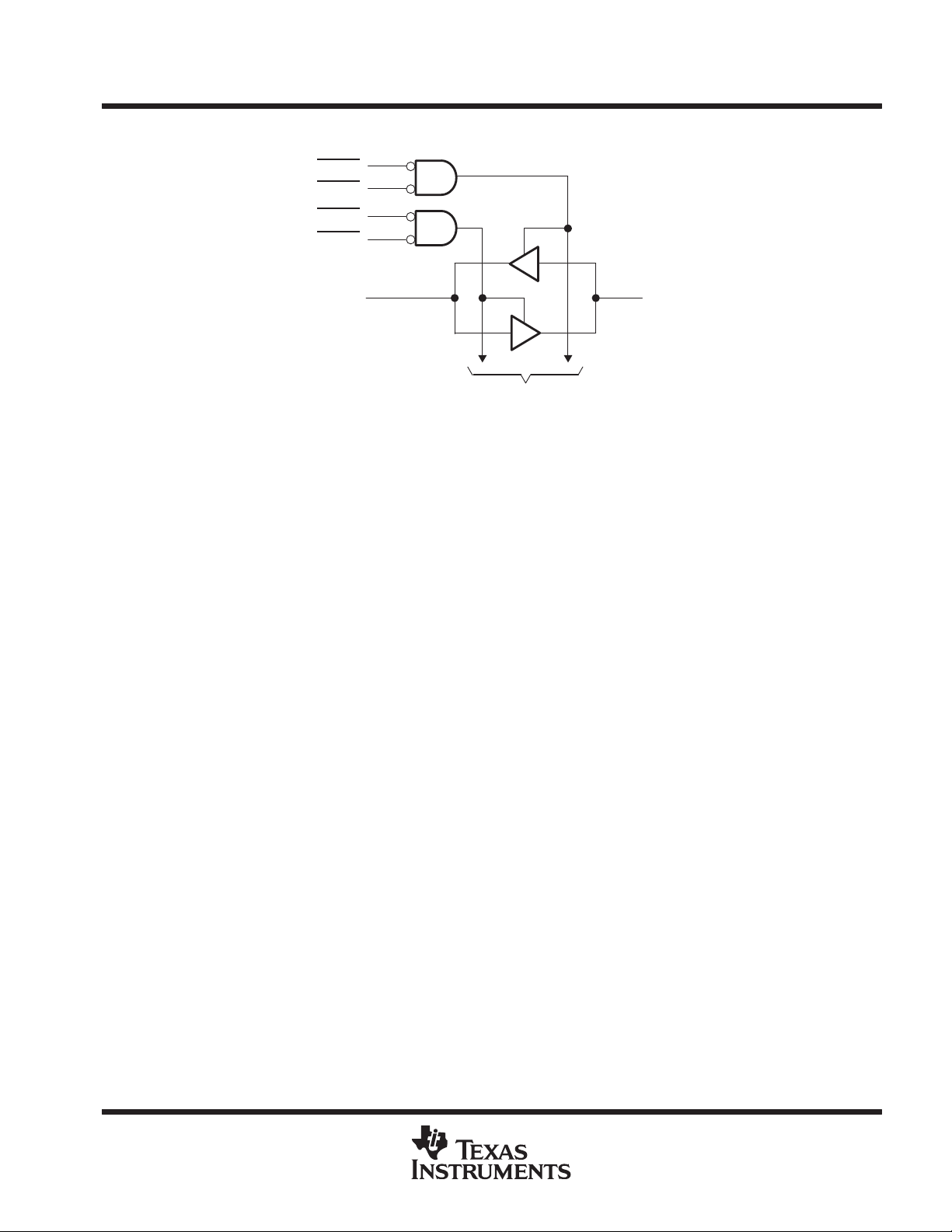
logic diagram (positive logic)
SN54ABT863, SN74ABT863
9-BIT BUS TRANSCEIVERS
WITH 3-STATE OUTPUTS
SCBS201E – FEBRUARY 1991 – REVISED JULY 1998
OEBA1
OEBA2
OEAB1
OEAB2
Pin numbers shown are for the DB, DW, JT, NT, and PW packages.
1
11
13
14
223
A1 B1
To Eight Other Channels
absolute maximum ratings over operating free-air temperature range (unless otherwise noted)
Supply voltage range, V
Input voltage range, V
Voltage range applied to any output in the high or power-off state, V
Current into any output in the low state, I
Input clamp current, I
Output clamp current, I
Package thermal impedance, θ
Storage temperature range, T
†
Stresses beyond those listed under “absolute maximum ratings” may cause permanent damage to the device. These are stress ratings only, and
functional operation of the device at these or any other conditions beyond those indicated under “recommended operating conditions” is not
implied. Exposure to absolute-maximum-rated conditions for extended periods may affect device reliability.
NOTES: 1. The input and output negative-voltage ratings may be exceeded if the input and output clamp-current ratings are observed.
2. The package thermal impedance is calculated in accordance with JESD 51, except for through-hole packages, which use a trace
length of zero.
–0.5 V to 7 V. . . . . . . . . . . . . . . . . . . . . . . . . . . . . . . . . . . . . . . . . . . . . . . . . . . . . . . . . .
CC
(except I/O ports) (see Note 1) –0.5 V to 7 V. . . . . . . . . . . . . . . . . . . . . . . . . . . . . . . . . .
I
: SN54ABT863 96 mA. . . . . . . . . . . . . . . . . . . . . . . . . . . . . . . . . . . .
O
–0.5 V to 5.5 V. . . . . . . . . . . . . . . . . . .
O
SN74ABT863 128 mA. . . . . . . . . . . . . . . . . . . . . . . . . . . . . . . . . . .
(VI < 0) –18 mA. . . . . . . . . . . . . . . . . . . . . . . . . . . . . . . . . . . . . . . . . . . . . . . . . . . . . . . . . . .
IK
(VO < 0) –50 mA. . . . . . . . . . . . . . . . . . . . . . . . . . . . . . . . . . . . . . . . . . . . . . . . . . . . . . . .
OK
(see Note 2): DB package 104°C/W. . . . . . . . . . . . . . . . . . . . . . . . . . . . . . . .
JA
DW package 81°C/W. . . . . . . . . . . . . . . . . . . . . . . . . . . . . . . . .
NT package 67°C/W. . . . . . . . . . . . . . . . . . . . . . . . . . . . . . . . .
PW package 120°C/W. . . . . . . . . . . . . . . . . . . . . . . . . . . . . . . .
–65°C to 150°C. . . . . . . . . . . . . . . . . . . . . . . . . . . . . . . . . . . . . . . . . . . . . . . . . . .
stg
†
POST OFFICE BOX 655303 • DALLAS, TEXAS 75265
3
SN54ABT863, SN74ABT863
UNIT
9-BIT BUS TRANSCEIVERS
WITH 3-STATE OUTPUTS
SCBS201E – FEBRUARY 1991 – REVISED JULY 1998
recommended operating conditions (see Note 3)
SN54ABT863 SN74ABT863
MIN MAX MIN MAX
V
CC
V
IH
V
IL
V
I
I
OH
I
OL
∆t/∆v Input transition rise or fall rate Outputs enabled 5 5 ns/V
∆t/∆V
T
A
NOTE 3: All unused inputs of the device must be held at VCC or GND to ensure proper device operation. Refer to the TI application report,
Supply voltage 4.5 5.5 4.5 5.5 V
High-level input voltage 2 2 V
Low-level input voltage 0.8 0.8 V
Input voltage 0 V
High-level output current –24 –32 mA
Low-level output current 48 64 mA
Power-up ramp rate 200 200 µs/V
CC
Operating free-air temperature –55 125 –40 85 °C
Implications of Slow or Floating CMOS Inputs
, literature number SCBA004.
CC
0 V
CC
V
PRODUCT PREVIEW information concerns products in the formative or
design phase of development. Characteristic data and other
specifications are design goals. Texas Instruments reserves the right to
change or discontinue these products without notice.
4
POST OFFICE BOX 655303 • DALLAS, TEXAS 75265
PARAMETER
TEST CONDITIONS
UNIT
V
V
V
4.5 V
VOLV
V
V
I
A
V
CC
¶
D
,
SN54ABT863, SN74ABT863
9-BIT BUS TRANSCEIVERS
WITH 3-STATE OUTPUTS
SCBS201E – FEBRUARY 1991 – REVISED JULY 1998
electrical characteristics over recommended operating free-air temperature range (unless
otherwise noted)
TA = 25°C SN54ABT863 SN74ABT863
MIN TYP†MAX MIN MAX MIN MAX
V
IK
OH
V
hys
I
I
OZPU
I
OZPD
I
OZH
I
OZL
I
off
I
CEX
I
O
I
CC
∆I
C
C
* On products compliant to MIL-PRF-38535, this parameter does not apply.
** On products compliant to MIL-PRF-38535, this parameter is not production tested.
†
All typical values are at VCC = 5 V.
‡
The parameters I
§
Not more than one output should be tested at a time, and the duration of the test should not exceed one second.
¶
This is the increase in supply current for each input that is at the specified TTL voltage level rather than VCC or GND.
Control inputs VCC = 0 to 5.5 V, VI = VCC or GND ±1 ±1 ±1
A or B ports VCC = 2.1 V to 5.5 V, VI = VCC or GND ±20 ±20 ±20
‡
‡
§
A or B ports
ata inputs
CC
Control inputs
Control inputs VI = 2.5 V or 0.5 V 4 pF
i
A or B ports VO = 2.5 V or 0.5 V 7 pF
io
OZH
VCC = 4.5 V, II = –18 mA –1.2 –1.2 –1.2 V
VCC = 4.5 V, IOH = –3 mA 2.5 2.5 2.5
VCC = 5 V, IOH = –3 mA 3 3 3
=
CC
= 4.5
CC
VCC = 0 to 2.1 V, VO = 0.5 V to 2.7 V,
OE
= * don’t care
VCC = 2.1 V to 0, VO = 0.5 V to 2.7 V,
OE
= * don’t care
VCC = 2.1 V to 5.5 V, VO = 2.7 V,
OE
≥ 2 V
VCC = 2.1 V to 5.5 V, VO = 0.5 V,
OE
≥ 2 V
VCC = 0, VI or VO ≤ 4.5 V ±100* ±100 µA
VCC = 5.5 V,
VO = 5.5 V
VCC = 5.5 V, VO = 2.5 V –50 –100 –225 –50 –225 –50 –225 mA
=
= 5.5 V,
IO = 0,
VI = VCC or GND
VCC = 5.5 V,
One input at 3.4 V ,
Other inputs at
VCC or GND
VCC = 5.5 V, One input at 3.4 V,
Other inputs at VCC or GND
and I
include the input leakage current.
OZL
IOH = –24 mA 2 2
IOH = –32 mA 2* 2
IOL = 48 mA 0.55 0.55
IOL = 64 mA 0.55* 0.55
100 mV
±50 ±50** ±50 µA
±50 ±50** ±50 µA
10 10 10 µA
–10 –10 –10 µA
Outputs high 50 50 50 µA
Outputs high 1 250 250 250 µA
Outputs low 24 30 38 38 mA
Outputs disabled 0.5 250 250 250 µA
Outputs enabled 1.5 1.5 1.5
Outputs disabled 0.05 0.05 0.05
1.5 1.5 1.5
µ
mA
PRODUCT PREVIEW information concerns products in the formative or
design phase of development. Characteristic data and other
specifications are design goals. Texas Instruments reserves the right to
change or discontinue these products without notice.
POST OFFICE BOX 655303 • DALLAS, TEXAS 75265
5

SN54ABT863, SN74ABT863
(INPUT)
(OUTPUT)
A or B
B or A
ns
OEAB
OEBA
B or A
ns
OEAB
OEBA
B or A
ns
9-BIT BUS TRANSCEIVERS
WITH 3-STATE OUTPUTS
SCBS201E – FEBRUARY 1991 – REVISED JULY 1998
switching characteristics over recommended ranges of supply voltage and operating free-air
temperature, C
PARAMETER
t
PLH
t
PHL
t
PZH
t
PZL
t
PHZ
t
PLZ
= 50 pF (unless otherwise noted) (see Figure 1)
L
FROM
or
or
TO
VCC = 5 V,
TA = 25°C
MIN TYP MAX MIN MAX MIN MAX
1 2.6 4.1 1 7 1 5.7
1 2.3 3.3 1 3.9 1 3.9
1 3.2 4.3 1 5.4 1 5.5
1 3.3 4.4 1 5.5 1 5.4
2.5 4.8 6 2.5 6.8 2.5 6.7
1.5 4.4 5.9 1.5 7.8 1.5 6.9
SN54ABT863 SN74ABT863
UNIT
PRODUCT PREVIEW information concerns products in the formative or
design phase of development. Characteristic data and other
specifications are design goals. Texas Instruments reserves the right to
change or discontinue these products without notice.
6
POST OFFICE BOX 655303 • DALLAS, TEXAS 75265
From Output
Under Test
CL = 50 pF
(see Note A)
SCBS201E – FEBRUARY 1991 – REVISED JULY 1998
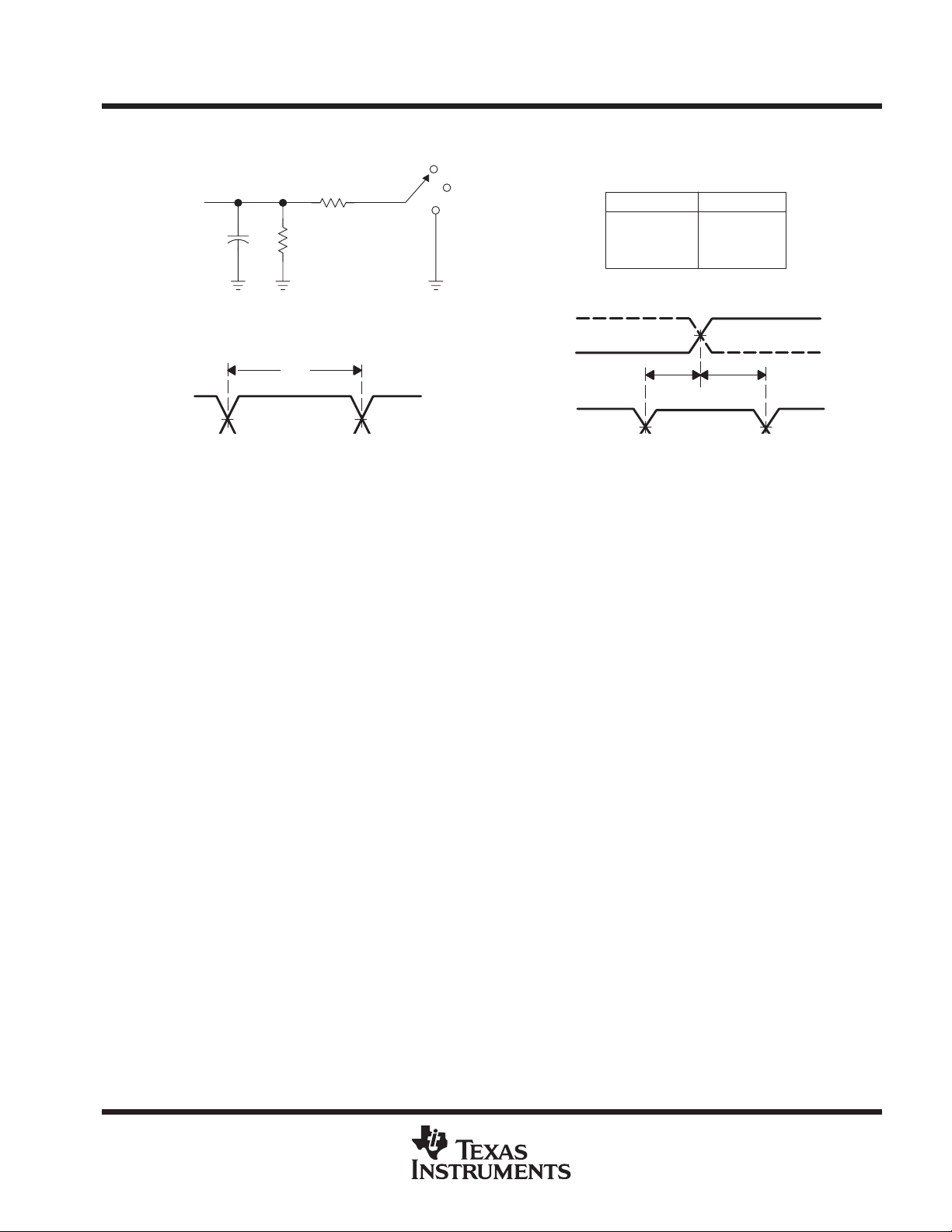
PARAMETER MEASUREMENT INFORMATION
7 V
500 Ω
500 Ω
S1
Open
GND
TEST S1
t
PLH/tPHL
t
PLZ/tPZL
t
PHZ/tPZH
SN54ABT863, SN74ABT863
9-BIT BUS TRANSCEIVERS
WITH 3-STATE OUTPUTS
Open
7 V
Open
Input
LOAD CIRCUIT
t
w
1.5 V 1.5 V
Figure 1. Load Circuit and Voltage Waveforms
3 V
Timing Input
Data Input
1.5 V
t
su
1.5 V 1.5 V
t
h
3 V
0 V
3 V
POST OFFICE BOX 655303 • DALLAS, TEXAS 75265
7

IMPORTANT NOTICE
T exas Instruments and its subsidiaries (TI) reserve the right to make changes to their products or to discontinue
any product or service without notice, and advise customers to obtain the latest version of relevant information
to verify, before placing orders, that information being relied on is current and complete. All products are sold
subject to the terms and conditions of sale supplied at the time of order acknowledgement, including those
pertaining to warranty, patent infringement, and limitation of liability.
TI warrants performance of its semiconductor products to the specifications applicable at the time of sale in
accordance with TI’s standard warranty. Testing and other quality control techniques are utilized to the extent
TI deems necessary to support this warranty . Specific testing of all parameters of each device is not necessarily
performed, except those mandated by government requirements.
CERT AIN APPLICATIONS USING SEMICONDUCTOR PRODUCTS MAY INVOLVE POTENTIAL RISKS OF
DEATH, PERSONAL INJURY, OR SEVERE PROPERTY OR ENVIRONMENTAL DAMAGE (“CRITICAL
APPLICATIONS”). TI SEMICONDUCTOR PRODUCTS ARE NOT DESIGNED, AUTHORIZED, OR
WARRANTED TO BE SUITABLE FOR USE IN LIFE-SUPPORT DEVICES OR SYSTEMS OR OTHER
CRITICAL APPLICA TIONS. INCLUSION OF TI PRODUCTS IN SUCH APPLICATIONS IS UNDERST OOD TO
BE FULLY AT THE CUSTOMER’S RISK.
In order to minimize risks associated with the customer’s applications, adequate design and operating
safeguards must be provided by the customer to minimize inherent or procedural hazards.
TI assumes no liability for applications assistance or customer product design. TI does not warrant or represent
that any license, either express or implied, is granted under any patent right, copyright, mask work right, or other
intellectual property right of TI covering or relating to any combination, machine, or process in which such
semiconductor products or services might be or are used. TI’s publication of information regarding any third
party’s products or services does not constitute TI’s approval, warranty or endorsement thereof.
Copyright 1998, Texas Instruments Incorporated
 Loading...