

Datasheet SN74ABT7820-15PH, SN74ABT7820-15PN, SN74ABT7820-20PH, SN74ABT7820-20PN, SN74ABT7820-25PH Datasheet (Texas Instruments)
...Page 1
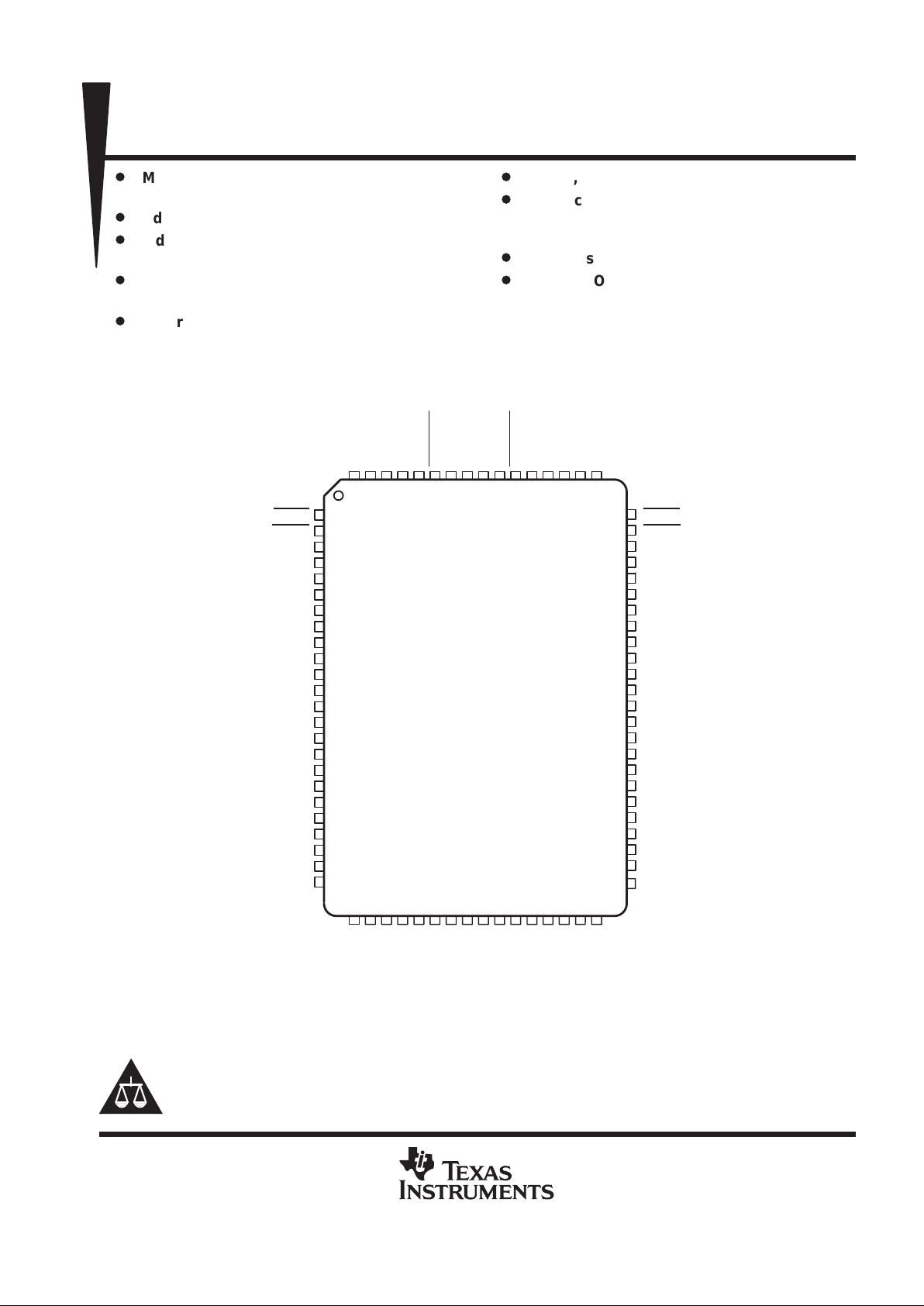
SN74ABT7820
512 × 18 × 2
STROBED BIDIRECTIONAL FIRST-IN, FIRST-OUT MEMORY
SCAS206D – AUGUST 1991 – REVISED APRIL 1998
1
POST OFFICE BOX 655303 • DALLAS, TEXAS 75265
D
Member of the Texas Instruments
Widebus Family
D
Advanced BiCMOS Technology
D
Independent Asynchronous Inputs and
Outputs
D
Two Separate 512 × 18 FIFOs Buffering
Data in Opposite Directions
D
Programmable Almost-Full/Almost-Empty
Flags
D
Empty, Full, and Half-Full Flags
D
Fast Access Times of 12 ns With a 50-pF
Load and Simultaneous Switching Data
Outputs
D
Supports Clock Rates up to 67 MHz
D
Package Options Include 80-Pin Quad Flat
(PH) and 80-Pin Thin Quad Flat (PN)
Packages
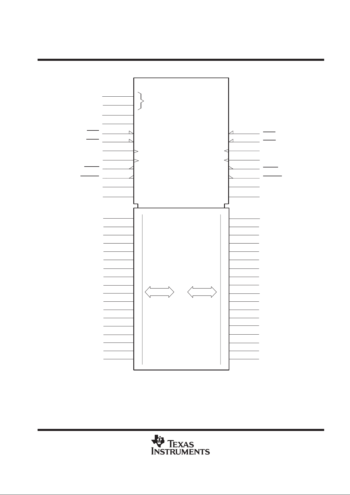
GBA
SBA
GND
LDCKA
UNCKB
EMPTYB
EMPTYA
UNCKA
LDCKB
GND
SAB
GAB
A12
A13
A14
V
CC
V
CC
A15
GND
GND
A16
A17
B17
B16
B15
B14
B13
B12
24
65
4025
41
641
RSTA
PENA
AF/AEA
HFA
FULLA
GND
A0
A1
V
CC
A2
A3
GND
A4
A5
GND
A6
A7
GND
A8
A9
V
CC
A10
A11
GND
2
3
4
5
6
7
8
9
10
11
12
13
14
15
16
17
18
19
20
21
22
23
26 27 28 29 30 3132 33 34 3536 37 38 39
8079 78 77 76 75 74 73 72 7170 69 68 6766
63
62
61
60
59
58
57
56
55
54
53
52
51
50
49
48
47
46
45
44
43
42
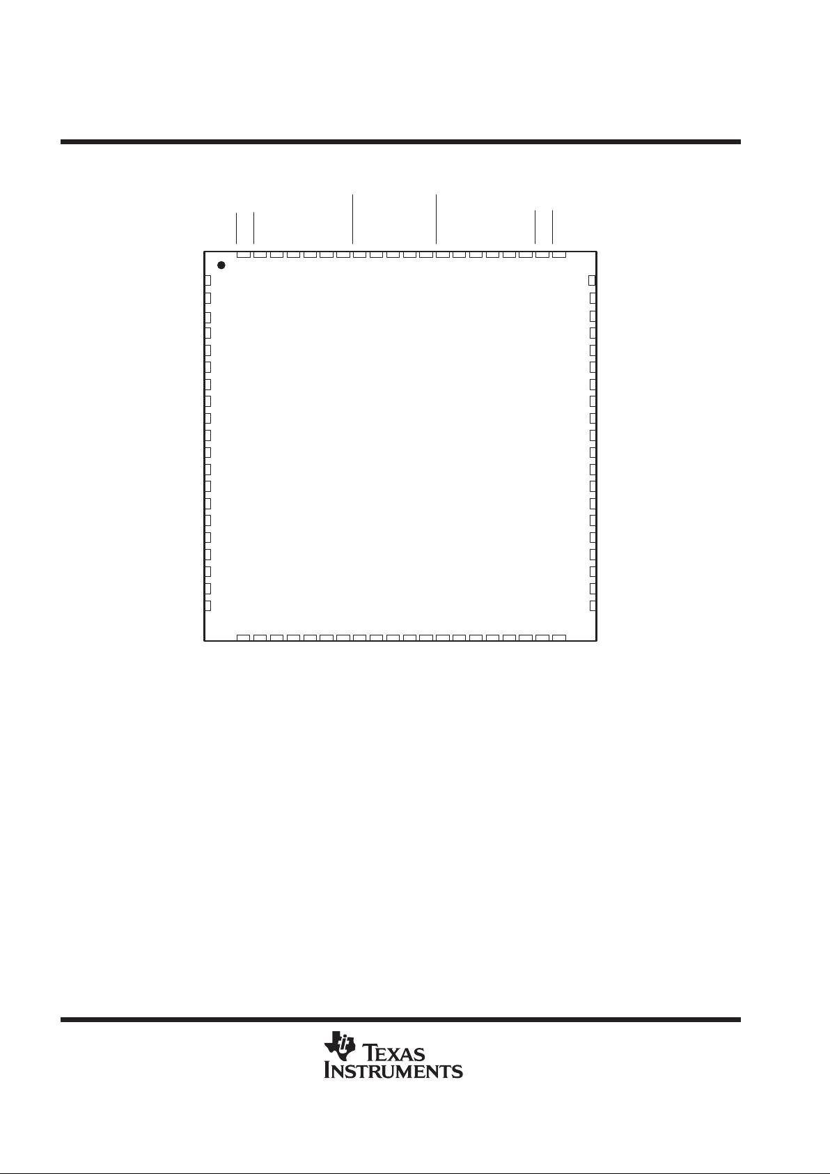
PH PACKAGE
(TOP VIEW)
RSTB
PENB
AF/AEB
HFB
FULLB
GND
B0
B1
V
CC
B2
B3
GND
B4
B5
GND
B6
B7
GND
B8
B9
V
CC
B10
B1 1
GND
CC
VCCVCCVCCV
Copyright 1998, Texas Instruments Incorporated
PRODUCTION DATA information is current as of publication date.
Products conform to specifications per the terms of Texas Instruments
standard warranty. Production processing does not necessarily include
testing of all parameters.
Please be aware that an important notice concerning availability, standard warranty, and use in critical applications of
Texas Instruments semiconductor products and disclaimers thereto appears at the end of this data sheet.
Widebus is a trademark of Texas Instruments Incorporated.
Page 2
SN74ABT7820
512 × 18 × 2
STROBED BIDIRECTIONAL FIRST-IN, FIRST-OUT MEMORY
SCAS206D – AUGUST 1991 – REVISED APRIL 1998
2
POST OFFICE BOX 655303 • DALLAS, TEXAS 75265
A11
GND
V
CC
A17
B11
A12
A13
GND
A14
A15
A16
B17
B16
GND
B15
B14
B13
B12
GND
PENB
SAB
GND
UNCKA
EMPTYA
EMPTYB
UNCKB
SBA
GBA
PENA
1
2
3
4
5
6
7
8
9
10
11
12
13
14
15
16
17
18
19
20
21 22 23 24 25
60
59
58
57
56
55
54
53
52
51
50
48
49
47
46
45
44
43
42
41
4026 27 28 29 30 31 32 33 34 35 36 37 38 39
80 79 78 77 76 75 74 73 71 70 69 68 67 66 65 64 63 62 6172
V
CC
PN PACKAGE
(TOP VIEW)
RSTB
GAB
LDCKB
LDCKA
GND
RSTA
AF/AEA
HFA
FULLA
GND
A0
A1
V
CC
A2
A3
GND
A4
A5
GND
A6
A7
GND
A8
A9
V
CC
A10
AF/AEB
HFB
FULLB
GND
B0
B1
V
CC
B2
B3
GND
B4
B5
GND
B6
B7
GND
B8
B9
V
CC
B10
CC
VCCVCCVCCV
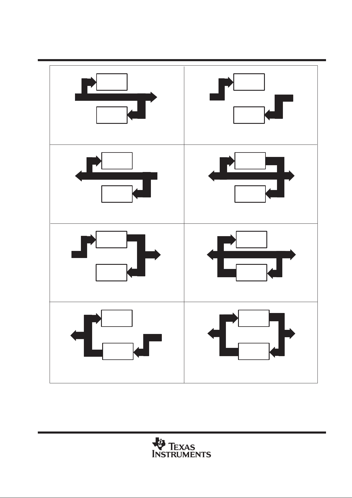
description
A FIFO memory is a storage device that allows data to be written into and read from its array at independent
data rates. The SN74ABT7820 is arranged as two 512 × 18-bit FIFOs for high speed and fast access times. It
processes data at rates up to 67 MHz with access times of 12 ns in a bit-parallel format.
The SN74ABT7820 consists of bus-transceiver circuits, two 512 × 18 FIFOs, and control circuitry arranged for
multiplexed transmission of data directly from the data bus or from the internal FIFO memories. Enable inputs
(GAB and GBA) control the transceiver functions. The SAB and SBA control inputs select whether real-time or
stored data is transferred. The circuitry used for select control eliminates the typical decoding glitch that occurs
in a multiplexer during the transition between stored and real-time data. Figure 1 illustrates the eight
fundamental bus-management functions that can be performed with the SN74ABT7820.
The SN74ABT7820 is characterized for operation from 0°C to 70°C.
Page 3
SN74ABT7820
512 × 18 × 2
STROBED BIDIRECTIONAL FIRST-IN, FIRST-OUT MEMORY
SCAS206D – AUGUST 1991 – REVISED APRIL 1998
3
POST OFFICE BOX 655303 • DALLAS, TEXAS 75265
FIFO A
Bus A
In
Bus B
Out
FIFO B
Out In
SABLSBAXGABHGBA
L
FIFO A
In Out
FIFO B
Out In
Bus A
Bus B
SABXSBALGABLGBA
H
SABHSBAXGABHGBA
L
SABXSBAHGABLGBA
H
SABXSBAXGABLGBA
L
SABHSBALGABHGBA
H
SABLSBAHGABHGBA
H
SABHSBAHGABHGBA
H
FIFO A
Bus A
In
Bus B
Out
FIFO B
Out In
FIFO A
Bus A
In
Bus B
Out
FIFO B
Out In
FIFO A
Bus A
In
Bus B
Out
FIFO B
Out In
FIFO A
Bus A
In
Bus B
Out
FIFO B
Out In
FIFO A
Bus A
In
Bus B
Out
FIFO B
Out In
FIFO A
In Out
FIFO B
Out In
Bus A
Bus B
Figure 1. Bus-Management Functions
Page 4
SN74ABT7820
512 × 18 × 2
STROBED BIDIRECTIONAL FIRST-IN, FIRST-OUT MEMORY
SCAS206D – AUGUST 1991 – REVISED APRIL 1998
4
POST OFFICE BOX 655303 • DALLAS, TEXAS 75265
SELECT-MODE CONTROL TABLE
CONTROL
OPERATION
SBA SAB A BUS B BUS
L L Real-time B-to-A bus Real-time A-to-B bus
H L FIFO B-to-A bus Real-time A-to-B bus
L H Real-time B-to-A bus FIFO A-to-B bus
H H FIFO B-to-A bus FIFO A-to-B bus
OUTPUT-ENABLE CONTROL TABLE
CONTROL
OPERATION
GBA GAB A BUS B BUS
L L Isolation/input to A bus Isolation/input to B bus
H L A bus enabled Isolation/input to B bus
L H Isolation/input to A bus B bus enabled
H H A bus enabled B bus enabled
Figure 1. Bus-Management Functions (Continued)
Page 5
SN74ABT7820
512 × 18 × 2
STROBED BIDIRECTIONAL FIRST-IN, FIRST-OUT MEMORY
SCAS206D – AUGUST 1991 – REVISED APRIL 1998
5
POST OFFICE BOX 655303 • DALLAS, TEXAS 75265
logic symbol
†
69
UNCKA
LDCKA
A1
63
PROG ENB
75
EMPTYB
PROG ENA
2
EMPTYA
70
FULLA
5
77
LDCKA
UNCKA
RESET A
1
EN2
80
GBA
EN1
65
GAB
0
79
SBA
1
66
SAB
60
FULLB
UNCKB
76
LDCKB
68
64
RESET B
A2
A3
A4
A5
A6
A7
B1
B2
B3
B4
B5
B6
B7
57
55
54
52
51
49
48
8
10
11
13
14
16
17
A8
19
B8
46
ALMOST FULL/
3
AF/AEA
ALMOST EMPTY A
AF/AEB
62
ALMOST FULL/
ALMOST EMPTY B
0
7
A0
B0
58
0
HALF-FULL A
4
HFA HFB
61
HALF-FULL B
A10
A11
A12
A13
A14
A15
A16
22
23
25
26
28
29
31
A17
32
20
A9
B10
B11
B12
B13
B14
B15
B16
43
42
40
39
37
36
34
B17
33
B9
45
A Data B Data
LDCKB
UNCKB
Φ
FIFO
512 × 18 × 2
SN74ABT7820
MODE
17
17
RSTA
PENA
FULLA
EMPTYA
RSTB
PENB
FULLB
EMPTYB
†
This symbol is in accordance with ANSI/IEEE Std 91-1984 and IEC Publication 617-12.
Pin numbers shown are for the PH package.
Page 6

SN74ABT7820
512 × 18 × 2
STROBED BIDIRECTIONAL FIRST-IN, FIRST-OUT MEMORY
SCAS206D – AUGUST 1991 – REVISED APRIL 1998
6
POST OFFICE BOX 655303 • DALLAS, TEXAS 75265
logic diagram (positive logic)
Q
D
Q
D
B0
1 of 18 Channels
SAB
SBA
EMPTYB
UNCKB
GBA
GAB
RSTA
PENA
FULLA
LDCKA
A0
RSTB
PENB
FULLB
LDCKB
To Other Channels
1 of 18 Channels
To Other Channels
EMPTYA
UNCKA
AF/AEA
AF/AEB
HFB
HFA
[1]
[2]
[3]
[4]
[15]
[16]
[17]
[18]
[1]
[2]
[3]
[4]
[15]
[16]
[17]
[18]
Φ
FIFO B
512 × 18
Φ
FIFO A
512 × 18
Page 7

SN74ABT7820
512 × 18 × 2
STROBED BIDIRECTIONAL FIRST-IN, FIRST-OUT MEMORY
SCAS206D – AUGUST 1991 – REVISED APRIL 1998
7
POST OFFICE BOX 655303 • DALLAS, TEXAS 75265
Terminal Functions
TERMINAL I/O DESCRIPTION
A0–A17 I/O Port-A data. The 18-bit bidirectional data port for side A.
AF/AEA O
FIFO A almost-full/almost-empty flag. Depth-offset values can be programmed for AF/AEA or the default value of 128 can
be used for both the almost-empty offset (X) and the almost-full offset (Y). AF/AEA is high when FIFO A contains X or
fewer words or (512 – Y) or more words. AF/AEA is set high after FIFO A is reset.
AF/AEB O
FIFO B almost-full/almost-empty flag. Depth-offset values can be programmed for AF/AEB or the default value of 128 can
be used for both the almost-empty offset (X) and the almost-full offset (Y). AF/AEB is high when FIFO B contains
X or fewer words or (512 – Y) or more words. AF/AEB is set high after FIFO B is reset.
B0–B17 I/O Port-B data. The 18-bit bidirectional data port for side B.
EMPTYA O
FIFO A empty flag. EMPTYA is low when FIFO A is empty and high when FIFO A is not empty. EMPTYA is set low after
FIFO A is reset.
EMPTYB O
FIFO B empty flag. EMPTYB is low when FIFO B is empty and high when FIFO B is not empty. EMPTYB is set low after
FIFO B is reset.
FULLA O FIFO A full flag. FULLA is low when FIFO A is full and high when FIFO A is not full. FULLA is set high after FIFO A is reset.
FULLB O FIFO B full flag. FULLB is low when FIFO B is full and high when FIFO B is not full. FULLB is set high after FIFO B is reset.
GAB I Port-B output enable. B0–B17 outputs are active when GAB is high and in the high-impedance state when GAB is low.
GBA I Port-A output enable. A0–A17 outputs are active when GBA is high and in the high-impedance state when GBA is low.
HFA O
FIFO A half-full flag. HFA is high when FIFO A contains 256 or more words and is low when FIFO A contains 255 or fewer
words. HFA is set low after FIFO A is reset.
HFB O
FIFO B half-full flag. HFB is high when FIFO B contains 256 or more words and is low when FIFO B contains 255 or fewer
words. HFB is set low after FIFO B is reset.
LDCKA I
FIFO A load clock. Data is written into FIFO A on a low-to-high transition of LDCKA when FULLA is high. The first word
written into an empty FIFO A is sent directly to the FIFO A data outputs.
LDCKB I
FIFO B load clock. Data is written into FIFO B on a low-to-high transition of LDCKB when FULLB is high. The first word
written into an empty FIFO B is sent directly to the FIFO B data outputs.
PENA I
FIFO A program enable. After reset and before a word is written into FIFO A, the binary value on A0–A7 is latched as
an AF/AEA offset value when PENA
is low and LDCKA is high.
PENB I
FIFO B program enable. After reset and before a word is written into FIFO B, the binary value on B0–B7 is latched as
an AF/AEB offset value when PENB
is low and LDCKB is high.
RSTA I FIFO A reset. A low level on RSTA resets FIFO A forcing EMPTYA low , HFA low, FULLA high, and AF/AEA high.
RSTB I FIFO B reset. A low level on RSTB resets FIFO B forcing EMPTYB low, HFB low, FULLB high, and AF/AEB high.
SAB I
Port-B read select. SAB selects the source of B0–B17 read data. A low level selects real-time data from A0–A17. A high
level selects the FIFO A output.
SBA I
Port-A read select. SBA selects the source of A0–A17 read data. A low level selects real-time data from B0 – B17. A high
level selects the FIFO B output.
UNCKA I FIFO A unload clock. Data is read from FIFO A on a low-to-high transition of UNCKA when EMPTYA is high.
UNCKB I FIFO B unload clock. Data is read from FIFO B on a low-to-high transition of UNCKB when EMPTYB is high.
Page 8

SN74ABT7820
512 × 18 × 2
STROBED BIDIRECTIONAL FIRST-IN, FIRST-OUT MEMORY
SCAS206D – AUGUST 1991 – REVISED APRIL 1998
8
POST OFFICE BOX 655303 • DALLAS, TEXAS 75265
Figure 2. Timing Diagram for FIFO A
ÎÎ
ÎÎ
ÎÎÎ
ÎÎÎ
ÎÎ
ÎÎ
ÎÎ
ÎÎ
ÎÎ
ÎÎ
ÎÎ
ÎÎ
ÎÎ
ÎÎ
ÎÎ
ÎÎ
ÎÎ
ÎÎ
ÎÎ
ÎÎ
ÎÎ
ÎÎ
ÎÎ
ÎÎ
ÎÎ
ÎÎ
ÎÎ
ÎÎ
ÎÎ
FULLA
EMPTYA
A0 – A17
PENA
Q0 – Q17
AF/AEA
HFA
LDCKA
UNCKA
Don’t Care
RSTA
Word
1
Word
2
Word
129
Word 1
Word
2
Word
129
Word
256
Word
384
Word
512
Word
257
Word
130
Word
258
Word
384
Word
385
Word
512
Set X = Y = 128 Empty + X FullHalf-Full Full – Y EmptyFull – Y Half-Full Empty + X
†
Operation of FIFO B is identical to that of FIFO A.
SAB = GAB = H, GBA = L
1
0
†
Invalid
Page 9

SN74ABT7820
512 × 18 × 2
STROBED BIDIRECTIONAL FIRST-IN, FIRST-OUT MEMORY
SCAS206D – AUGUST 1991 – REVISED APRIL 1998
9
POST OFFICE BOX 655303 • DALLAS, TEXAS 75265
offset values for AF/AEFigure 2
The AF/AE flag of each FIFO has two programmable limits: the almost-empty offset value (X) and the almost-full
offset value (Y). The offsets of a flag can be programmed from the input of its FIFO after it is reset and before
any data is written to its memory . An AF/AE flag is high when its FIFO contains X or fewer words or (512 – Y)
or more words.
T o program the offset values for AF/AEA, program enable (PENA
) can be brought low after FIFO A is reset and
only when LDCKA is low. On the following low-to-high transition of LDCKA, the binary value on A0–A7 is stored
as the almost-empty offset value (X) and the almost-full offset value (Y). Holding PENA
low for another
low-to-high transition of LDCKA reprograms Y to the binary value on A0–A7 at the time of the second LDCKA
low-to-high transition.
PENA
can be brought back high only when LDCKA is low during the first two LDCKA cycles. PENA can be
brought high at any time after the second LDCKA pulse returns low. A maximum value of 255 can be
programmed for either X or Y (see Figure 3). To use the default values of X = Y = 128 for AF/AEA, PENA
must
be tied high. No data is stored in the FIFO when its AF/AE offsets are programmed. The AF/AEB flag is
programmed in the same manner. PENB
enables LDCKB to program the AF/AEB offset values taken from
B0 –B7.
МММММ
МММММ
RSTA
ОООООООО
X and Y Y
PENA
A0–A17
EMPTYA
1
2
LDCKA
Word 1
Figure 3. Programming X and Y Separately for AF/AEA
Page 10

SN74ABT7820
512 × 18 × 2
STROBED BIDIRECTIONAL FIRST-IN, FIRST-OUT MEMORY
SCAS206D – AUGUST 1991 – REVISED APRIL 1998
10
POST OFFICE BOX 655303 • DALLAS, TEXAS 75265
absolute maximum ratings over operating free-air temperature (unless otherwise noted)
†
Supply voltage range, V
CC
–0.5 V to 7 V. . . . . . . . . . . . . . . . . . . . . . . . . . . . . . . . . . . . . . . . . . . . . . . . . . . . . . . . . .
Input voltage range, V
I
(see Note 1) –0.5 V to VCC + 0.5 V. . . . . . . . . . . . . . . . . . . . . . . . . . . . . . . . . . . . . . . . . .
Voltage range applied to any output in the high state or power-off state, V
O
–0.5 V to 5.5 V. . . . . . . . . . . . . .
Current into any output in the low state, I
O
48 mA. . . . . . . . . . . . . . . . . . . . . . . . . . . . . . . . . . . . . . . . . . . . . . . . . .
Input clamp current, I
IK
(VI < 0) –18 mA. . . . . . . . . . . . . . . . . . . . . . . . . . . . . . . . . . . . . . . . . . . . . . . . . . . . . . . . . . .
Output clamp current, I
OK
(VO < 0) –50 mA. . . . . . . . . . . . . . . . . . . . . . . . . . . . . . . . . . . . . . . . . . . . . . . . . . . . . . . .
Package thermal impedance, θ
JA
(see Note 2): PH package 76°C/W. . . . . . . . . . . . . . . . . . . . . . . . . . . . . . . . .
PN package 62°C/W. . . . . . . . . . . . . . . . . . . . . . . . . . . . . . . . .
Storage temperature range, T
stg
–65°C to 150°C. . . . . . . . . . . . . . . . . . . . . . . . . . . . . . . . . . . . . . . . . . . . . . . . . . .
†
Stresses beyond those listed under “absolute maximum ratings” may cause permanent damage to the device. These are stress ratings only, and
functional operation of the device at these or any other conditions beyond those indicated under “recommended operating conditions” is not
implied. Exposure to absolute-maximum-rated conditions for extended periods may affect device reliability.
NOTES: 1. The input and output negative-voltage ratings may be exceeded if the input and output clamp-current ratings are observed.
2. The package thermal impedance is calculated in accordance with JESD 51.
recommended operating conditions
MIN NOM MAX UNIT
V
CC
Supply voltage 4.5 5 5.5 V
V
IH
High-level input voltage 2 V
V
IL
Low-level input voltage 0.8 V
V
I
Input voltage 0 V
CC
V
I
OH
High-level output current –12 mA
I
OL
Low-level output current 24 mA
∆t/∆v Input transition rise or fall rate 5 ns/V
T
A
Operating free-air temperature 0 70 °C
Page 11

SN74ABT7820
512 × 18 × 2
STROBED BIDIRECTIONAL FIRST-IN, FIRST-OUT MEMORY
SCAS206D – AUGUST 1991 – REVISED APRIL 1998
11
POST OFFICE BOX 655303 • DALLAS, TEXAS 75265
electrical characteristics over recommended operating free-air temperature range (unless
otherwise noted)
PARAMETER TEST CONDITIONS MIN TYP†MAX UNIT
V
IK
VCC = 4.5 V, II = – 18 mA –1.2 V
VCC = 4.5 V, IOH = – 3 mA 2.5
V
OH
VCC = 5 V, IOH = – 3 mA 3
V
VCC = 4.5 V, IOH = – 12 mA 2
V
OL
VCC = 4.5 V, IOL = 24 mA 0.55 V
I
I
VCC = 5.5 V, VI = VCC or GND ±5 µA
I
OZH
‡
VCC = 5.5 V, VO = 2.7 V 50 µA
I
OZL
‡
VCC = 5.5 V, VO = 0.5 V –50 µA
I
O
§
VCC = 5.5 V, VO = 2.5 V –40 –100 –180 mA
Outputs high 15
I
CC
VCC = 5.5 V, IO = 0, VI = VCC or GND
Outputs low
95
mA
Outputs disabled 15
C
i
Control inputs VI = 2.5 V or 0.5 V 6 pF
C
o
Flags VO = 2.5 V or 0.5 V 4 pF
C
io
A or B ports VO = 2.5 V or 0.5 V 8 pF
†
All typical values are at VCC = 5 V, TA = 25°C.
‡
The parameters I
OZH
and I
OZL
include the input leakage current.
§
Not more than one output should be tested at a time, and the duration of the test should not exceed one second.
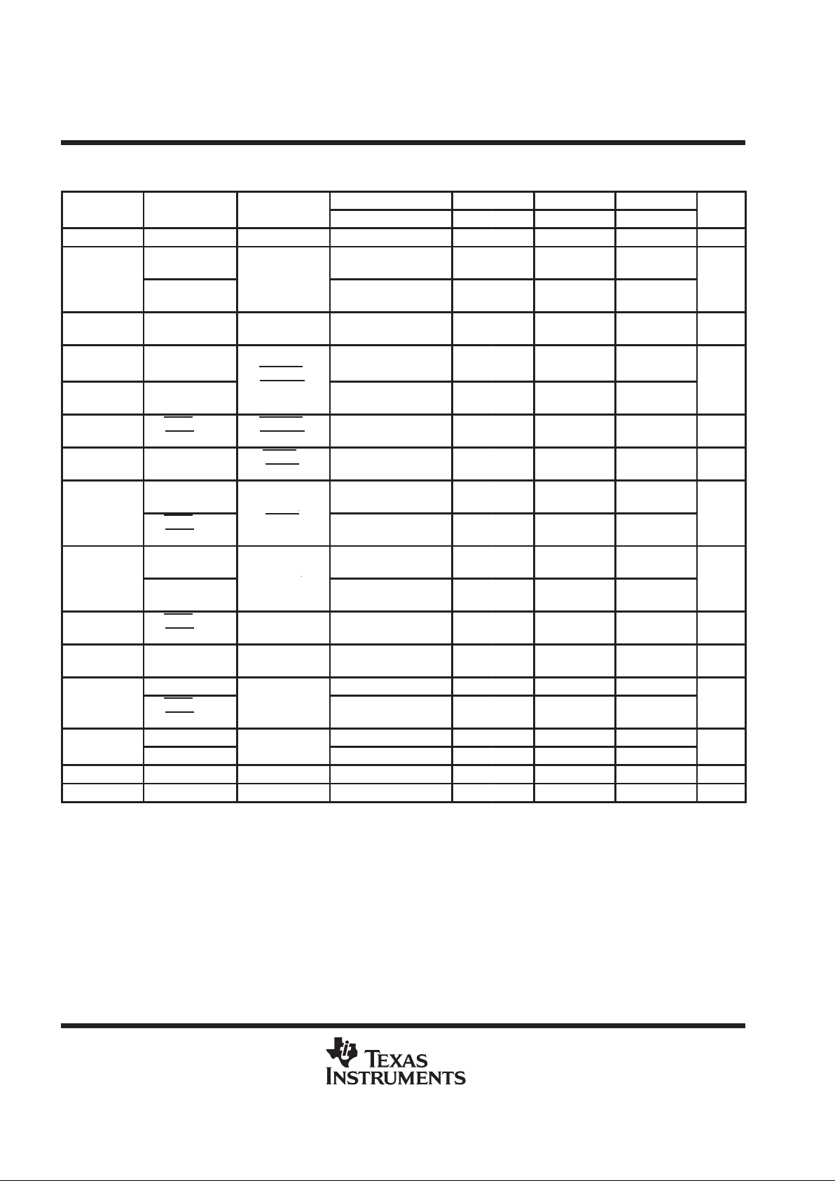
timing requirements over recommended operating free-air temperature range (unless otherwise
noted) (see Figures 2 through 4)
’ABT7820-15 ’ABT7820-20 ’ABT7820-25 ’ABT7820-30
MIN MAX MIN MAX MIN MAX MIN MAX
UNIT
f
clock
Clock frequency 67 50 40 33 MHz
LDCKA, LDCKB high 4 6 9 11
LDCKA, LDCKB low 4 6 9 11
t
w
Pulse
UNCKA, UNCKB high 4 6 9 11
ns
duration
UNCKA, UNCKB low 4 6 9 11
RSTA, RSTB low 6 8 10 12
A0–A17 before LDCKA↑ and
B0–B17 before LDCKB↑
3 4 4 4
t
su
Setup time
PENA
before LDCKA↑ and
PENB
before LDCKB↑
5 5 5 5
ns
LDCKA inactive before RSTA high
and LDCKB inactive before RSTB
high
3 3 4 4
A0–A17 after LDCKA↑ and
B0–B17 after LDCKB↑
0 0 0 0
t
h
Hold time
PENA
after LDCKA low and
PENB
after LDCKB low
2 2 2 2
ns
LDCKA inactive after RSTA high and
LDCKB inactive after RSTB
high
3 3 4 4
Page 12
SN74ABT7820
512 × 18 × 2
STROBED BIDIRECTIONAL FIRST-IN, FIRST-OUT MEMORY
SCAS206D – AUGUST 1991 – REVISED APRIL 1998
12
POST OFFICE BOX 655303 • DALLAS, TEXAS 75265
switching characteristics over recommended ranges of supply voltage and operating free-air
temperature, C
L
= 50 pF (unless otherwise noted) (see Figure 5)
FROM TO
’ACT7820-15 ’ACT7820-20 ’ACT7820-25 ’ACT7820-30
PARAMETER
(INPUT) (OUTPUT)
MIN TYP†MAX MIN MAX MIN MAX MIN MAX
UNIT
f
max
LDCK, UNCK 67 50 40 33.3 MHz
LDCKA↑,
LDCKB↑
4 14 4 15 4 18 4 20
t
pd
UNCKA↑,
UNCKB↑
B/A
4 9 12 4 13.5 4 15 4 17
ns
t
pd
‡
UNCKA↑,
UNCKB↑
B/A 8 ns
LDCKA↑,
t
PLH
LDCKB↑
EMPTYA,
4144154174
19
t
PHL
UNCKA↑,
UNCKB↑
EMPTYB
4 13 4 14 4 16 4 18
ns
t
PHL
RSTA low,
RSTB
low
EMPTYA,
EMPTYB
6 16 6 16 6 18 6 20 ns
t
PHL
LDCKA↑,
LDCKB↑
FULLA,
FULLB
6 13 6 14 6 16 6 18 ns
UNCKA↑,
UNCKB↑
FULLA,
6 15 6 15 6 17 6 19
t
PLH
RSTA low,
RSTB
low
,
FULLB
8 20 8 20 8 22 8 22
ns
LDCKA↑,
LDCKB↑
AF/AEA,
8 16 8 17 8 18 8 20
t
pd
UNCKA↑,
UNCKB↑
,
AF/AEB
8 16 8 17 8 18 8 20
ns
t
PLH
RSTA low,
RSTB
low
AF/AEA,
AF/AEB
2 12 2 14 2 16 2 18 ns
t
PLH
LDCKA↑,
LDCKB↑
HFA, HFB 8 15 8 15 8 17 8 19 ns
UNCKA, UNCKB 8 15 8 15 8 17 8 19
t
PHL
RSTA low,
RSTB
low
HFA, HFB
2 12 2 14 2 16 2 18
ns
SAB/SBA
§
2 10 2 11 2 12 2 14
t
pd
A/B
B/A
2 9 2 10 2 11 2 13
ns
t
en
GBA/GAB A/B 2 6.5 2 8 2 10 2 12 ns
t
dis
GBA/GAB A/B 2 11 2 12 2 13 2 14 ns
†
All typical values are at 5 V, TA = 25°C.
‡
This parameter is measured with a 30-pF load (see Figure 5).
§
These parameters are measured with the internal output state of the storage register opposite that of the bus input.
Page 13

SN74ABT7820
512 × 18 × 2
STROBED BIDIRECTIONAL FIRST-IN, FIRST-OUT MEMORY
SCAS206D – AUGUST 1991 – REVISED APRIL 1998
13
POST OFFICE BOX 655303 • DALLAS, TEXAS 75265
PARAMETER MEASUREMENT INFORMATION
V
OH
V
OL
t
h
t
PLH
t
PHL
Output
Control
Output
Waveform 1
S1 at 7 V
Output
Waveform 2
S1 at Open
t
PZL
t
PZH
t
PLZ
t
PHZ
1.5 V1.5 V
1.5 V 1.5 V
3 V
0 V
1.5 V 1.5 V
V
OH
V
OL
0 V
1.5 V
VOL + 0.3 V
1.5 V
VOH – 0.3 V
≈ 0 V
1.5 V
3 V
0 V
1.5 V 1.5 V
0 V
3 V
0 V
1.5 V 1.5 V
t
w
Input
3 V
3 V
≈ 3.5 V
VOLTAGE WAVEFORMS
SETUP AND HOLD TIMES
VOLTAGE WAVEFORMS
PROPAGATION DELAY TIMES
VOLTAGE WAVEFORMS
PULSE DURATION
VOLTAGE WAVEFORMS
ENABLE AND DISABLE TIMES
Timing
Input
Data
Input
Output
Input
S1
500 Ω
LOAD CIRCUIT
500 Ω
7 V
From Output
Under Test
Test
Point
NOTE A: CL includes probe and jig capacitance.
CL = 50 pF
(see Note A)
t
su
t
PZH
t
PZL
t
PHZ
t
PLZ
t
PLH
t
PHL
Open
Closed
Open
Closed
Open
Open
PARAMETER S1
t
en
t
dis
t
pd
Figure 4. Load Circuit and Voltage Waveforms
Page 14

SN74ABT7820
512 × 18 × 2
STROBED BIDIRECTIONAL FIRST-IN, FIRST-OUT MEMORY
SCAS206D – AUGUST 1991 – REVISED APRIL 1998
14
POST OFFICE BOX 655303 • DALLAS, TEXAS 75265
TYPICAL CHARACTERISTICS
typ + 2
typ
typ – 2
0 50 100 150
– Propagation Delay Time – ns
typ + 4
typ + 6
PROPAGATION DELAY TIME
vs
LOAD CAPACITANCE
200 250 300
t
pd
CL – Load Capacitance – pF
VCC = 5 V
TA = 25°C
RL = 500 Ω
Figure 5
100
80
60
20
10 15 20 25 30 35 40
– Supply Current – mA
120
140
SUPPLY CURRENT
vs
CLOCK FREQUENCY
160
45 50 65 70
40
55 60
f
clock
– Clock Frequency – MHz
CC(f)
I
VCC = 5 V
VCC = 5.5 V
TA = 75°C
CL = 0 pF
VCC = 4.5 V
Figure 6
Page 15

IMPORTANT NOTICE
T exas Instruments and its subsidiaries (TI) reserve the right to make changes to their products or to discontinue
any product or service without notice, and advise customers to obtain the latest version of relevant information
to verify, before placing orders, that information being relied on is current and complete. All products are sold
subject to the terms and conditions of sale supplied at the time of order acknowledgement, including those
pertaining to warranty, patent infringement, and limitation of liability.
TI warrants performance of its semiconductor products to the specifications applicable at the time of sale in
accordance with TI’s standard warranty. Testing and other quality control techniques are utilized to the extent
TI deems necessary to support this warranty. Specific testing of all parameters of each device is not necessarily
performed, except those mandated by government requirements.
CERT AIN APPLICATIONS USING SEMICONDUCTOR PRODUCTS MA Y INVOLVE POTENTIAL RISKS OF
DEATH, PERSONAL INJURY, OR SEVERE PROPERTY OR ENVIRONMENTAL DAMAGE (“CRITICAL
APPLICATIONS”). TI SEMICONDUCTOR PRODUCTS ARE NOT DESIGNED, AUTHORIZED, OR
WARRANTED TO BE SUITABLE FOR USE IN LIFE-SUPPORT DEVICES OR SYSTEMS OR OTHER
CRITICAL APPLICATIONS. INCLUSION OF TI PRODUCTS IN SUCH APPLICA TIONS IS UNDERST OOD TO
BE FULLY AT THE CUSTOMER’S RISK.
In order to minimize risks associated with the customer’s applications, adequate design and operating
safeguards must be provided by the customer to minimize inherent or procedural hazards.
TI assumes no liability for applications assistance or customer product design. TI does not warrant or represent
that any license, either express or implied, is granted under any patent right, copyright, mask work right, or other
intellectual property right of TI covering or relating to any combination, machine, or process in which such
semiconductor products or services might be or are used. TI’s publication of information regarding any third
party’s products or services does not constitute TI’s approval, warranty or endorsement thereof.
Copyright 1999, Texas Instruments Incorporated
 Loading...