

Datasheet SN74ABT3614-15PCB, SN74ABT3614-15PQ, SN74ABT3614-20PCB, SN74ABT3614-20PQ, SN74ABT3614-30PCB Datasheet (Texas Instruments)
...
SN74ABT3614
64 × 36 × 2 CLOCKED BIDIRECTIONAL FIRST-IN, FIRST-OUT MEMORY
WITH BUS MATCHING AND BYTE SWAPPING
SCBS126H – JUNE 1992 – REVISED APRIL 2000
1
POST OFFICE BOX 655303 • DALLAS, TEXAS 75265
D
Free-Running CLKA and CLKB Can Be
Asynchronous or Coincident
D
Two Independent 64 × 36 Clocked FIFOs
Buffering Data in Opposite Directions
D
Mailbox-Bypass Register for Each FIFO
D
Dynamic Port-B Bus Sizing of 36 Bits (Long
Word), 18 Bits (Word), and 9 Bits (Byte)
D
Selection of Big- or Little-Endian Format for
Word and Byte Bus Sizes
D
Three Modes of Byte-Order Swapping on
Port B
D
Programmable Almost-Full and
Almost-Empty Flags
D
Microprocessor Interface Control Logic
D
EFA, FFA, AEA, and AFA Flags
Synchronized by CLKA
D
EFB, FFB, AEB, and AFB Flags
Synchronized by CLKB
D
Passive Parity Checking on Each Port
D
Parity Generation Can Be Selected for Each
Port
D
Low-Power Advanced BiCMOS Technology
D
Supports Clock Frequencies up to 67 MHz
D
Fast Access Times of 10 ns
D
Package Options Include 120-Pin Thin
Quad Flat (PCB) and 132-Pin Quad Flat
(PQ) Packages
description
The SN74ABT3614 is a high-speed, low-power BiCMOS bidirectional clocked FIFO memory . It supports clock
frequencies up to 67 MHz and has read-access times as fast as 10 ns. Two independent 64 × 36 dual-port SRAM
FIFOs in this device buffer data in opposite directions. Each FIFO has flags to indicate empty and full conditions
and two programmable flags, almost full (AF) and almost empty (AE) to indicate when a selected number of
words is stored in memory . FIFO data on port B can be input and output in 36-bit, 18-bit, and 9-bit formats, with
a choice of big- or little-endian configurations. Three modes of byte-order swapping are possible with any
bus-size selection. Communication between each port can bypass the FIFOs via two 36-bit mailbox registers.
Each mailbox register has a flag to signal when new mail has been stored. Parity is checked passively on each
port and can be ignored if not desired. Parity generation can be selected for data read from each port.
The SN74ABT3614 is a clocked FIFO, which means each port employs a synchronous interface. All data
transfers through a port are gated to the low-to-high transition of a continuous (free-running) port clock by enable
signals. The continuous clocks for each port are independent of one another and can be asynchronous or
coincident. The enables for each port are arranged to provide a simple bidirectional interface between
microprocessors and/or buses controlled by a synchronous interface.
The full flag and almost-full flag of a FIFO are two-stage synchronized to the port clock that writes data to its
array . The empty flag and almost-empty flag of a FIFO are two-stage synchronized to the port clock that reads
data from its array.
The SN74ABT3614 is characterized for operation from 0°C to 70°C.
For more information on this device family, see the following application reports:
•
FIFO Mailbox-Bypass Registers: Using Bypass Registers to Initialize DMA Control
(literature number SCAA007)
•
Advanced Bus-Matching/Byte-Swapping Features for Internetworking FIFO Applications
(literature
number SCAA014)
•
Parity-Generate and Parity-Check Features for High-Bandwidth-Computing FIFO Applications
(literature number SCAA015)
•
Internetworking the SN74ABT3614
(literature number SCAA015)
•
Metastability Performance of Clocked FIFOs
(literature number SCZA004)
Copyright 2000, Texas Instruments Incorporated
PRODUCTION DATA information is current as of publication date.
Products conform to specifications per the terms of Texas Instruments
standard warranty. Production processing does not necessarily include
testing of all parameters.
Please be aware that an important notice concerning availability, standard warranty, and use in critical applications of
Texas Instruments semiconductor products and disclaimers thereto appears at the end of this data sheet.
SN74ABT3614
64 × 36 × 2 CLOCKED BIDIRECTIONAL FIRST-IN, FIRST-OUT MEMORY
WITH BUS MATCHING AND BYTE SWAPPING
SCBS126H – JUNE 1992 – REVISED APRIL 2000
2
POST OFFICE BOX 655303 • DALLAS, TEXAS 75265
1
2
3
4
5
6
7
8
9
10
11
12
13
14
15
16
17
18
19
20
21
22
23
24
25
26
27
28
29
93
94
95
96
97
98
99
100
101
102
103
104
105
106
107
108
109
110
111
112
113
114
115
116
117
118
119
120
90
89
88
87
86
85
84
83
82
81
80
79
78
77
76
75
74
73
72
71
70
69
68
67
66
65
64
63
62
59
58
57
56
55
54
53
52
51
50
49
48
47
46
45
44
43
42
41
40
39
38
37
36
35
34
33
32
31
91
92
60
30
61
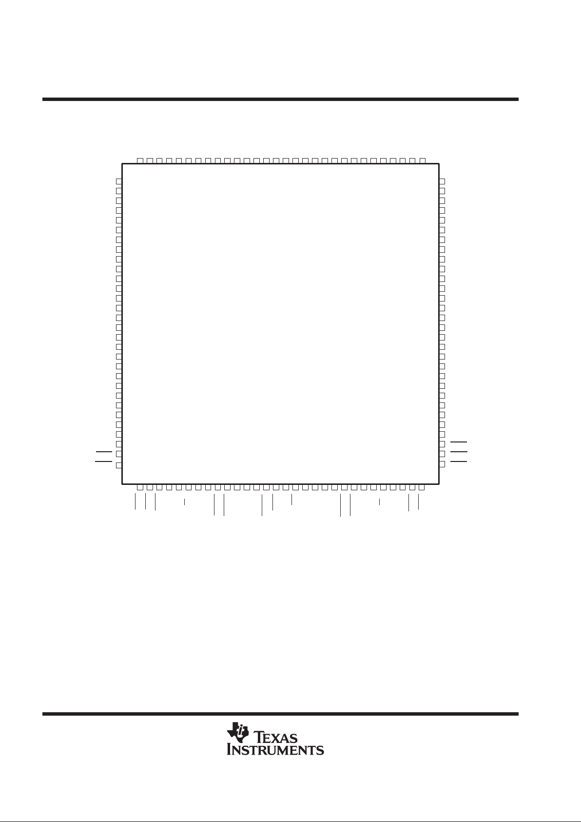
A24
A25
A26
A27
A28
GND
A30
A31
A32
A34
A35
GND
B35
B34
B33
B32
B31
B30
GND
B29
B28
B27
B26
B25
B24
B23
AFA
FFA
CSA
CLKA
W/RA
PEFA
MBF2
MBA
FS1
FS0
ODD/EVEN
RST
GND
SW1
SW0
SIZ0
MBF1
PEFB
PGB
W/RB
CLKB
ENB
CSB
CC
V
CC
V
CC
V
BE
PCB PACKAGE
(TOP VIEW)
A33
CC
V
FFB
SIZ1
PGA
B22
B21
GND
B20
B19
B18
B17
B16
B15
B14
B13
B12
B11
B10
GND
B9
B8
B7
V
CC
B6
B5
B4
B3
GND
B2
B1
B0
EFB
AEB
AFB
A23
A22
A21
GND
A20
A19
A18
A17
A16
A15
A14
A13
A12
A11
A10
GND
A9
A8
A7
V
CC
A6
A5
A4
A3
GND
A2
A1
A0
EFA
AEA
A29
ENA
SN74ABT3614
64 × 36 × 2 CLOCKED BIDIRECTIONAL FIRST-IN, FIRST-OUT MEMORY
WITH BUS MATCHING AND BYTE SWAPPING
SCBS126H – JUNE 1992 – REVISED APRIL 2000
3
POST OFFICE BOX 655303 • DALLAS, TEXAS 75265
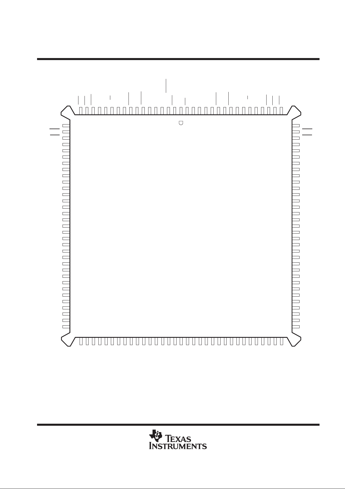
132
131
130
129
128
127
126
125
124
123
122
121
120
119
118
117
116
115
114
113
112
111
110
109
108
107
106
105
104
103
102
101
100
99
98
97
96
95
94
93
92
91
90
89
88
87
86
85
84
5251 83828180797877767574737271706968676665646362616059585756555453
50
49
48
47
46
45
44
43
42
41
40
39
38
37
36
35
34
33
32
31
30
29
28
27
26
25
24
23
22
21
20
19
18
17 16 15 14 13 12 11 10 9 8 7 6 5 4 3 2
1
GND
AEA
EFA
A0
A1
A2
GND
A3
A4
A5
A6
V
CC
A7
A8
A9
GND
A10
A11
V
CC
A12
A13
A14
GND
A15
A16
A17
A18
A19
A20
GND
A21
A22
A23
GND
AEB
EFB
B0
B1
B2
GND
B3
B4
B5
B6
V
CC
B7
B8
B9
GND
B10
B11
V
CC
B12
B13
B14
GND
B15
B16
B17
B18
B19
B20
GND
B21
B22
B23
PQ PACKAGE
†
(TOP VIEW)
AFA
FFAVENA
CLKA
W/RA
PGA
PEFA
GND
MBF2
MBA
FS0
ODD/EVEN
RST
GNDBESW1
SW0
SIZ1
SIZ0
MBF1
GND
PGB
W/RB
CLKB
ENB
CSB
FFB
AFB
A24
A25
A26
GND
A27
A29
A30
A31
A32
GND
A33
A34
A35
GND
B35
B34
GND
B32
B31
B30
B29
B28
B27
GND
B26
B25
B24
CC
A28
B33
CC
V
CSA
FS1
PEFB
CC
V
V
CC
CC
V
CC
V
NC – No internal connection
†
Uses Yamaichi socket IC51-1324-828
SN74ABT3614
64 × 36 × 2 CLOCKED BIDIRECTIONAL FIRST-IN, FIRST-OUT MEMORY
WITH BUS MATCHING AND BYTE SWAPPING
SCBS126H – JUNE 1992 – REVISED APRIL 2000
4
POST OFFICE BOX 655303 • DALLAS, TEXAS 75265
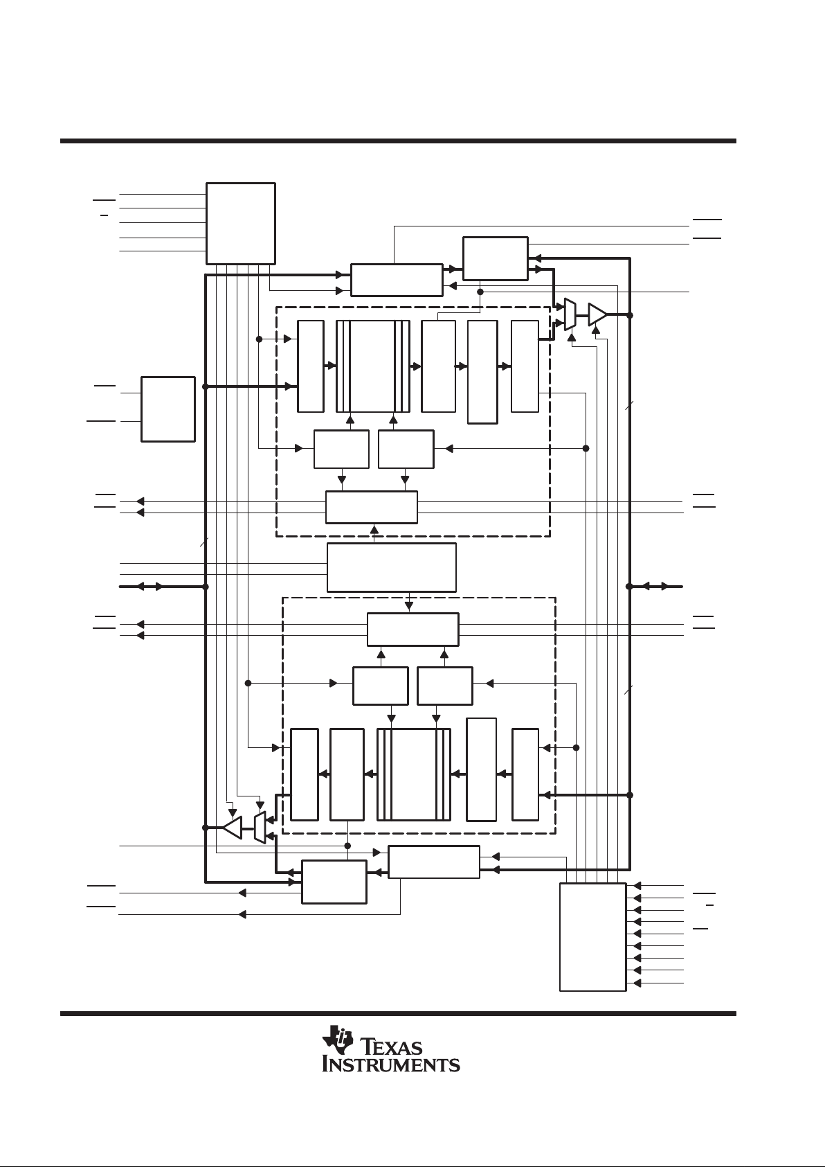
functional block diagram
Port-A
Control
Logic
AFA
FIFO1
Programmable-Flag
Offset Register
Read
Pointer
64 × 36
SRAM
Port-B
Control
Logic
BE
Parity
Gen/Check
Write
Pointer
Mail2
Register
FIFO2
Status-Flag
Logic
Status-Flag
Logic
Write
Pointer
CLKA
CSA
W/RA
ENA
MBA
FFA
FS0
A0–A35
EFA
AEA
Device
Control
64 × 36
SRAM
Output Register
Mail1
Register
Read
Pointer
Input Register
Output Register
FS1
MBF2
AEB
CLKB
CSB
ENB
36
36
RST
MBF1
EFB
B0–B35
FFB
AFB
PEFB
PGB
ODD/
EVEN
Input Register
W/RB
Parity
Gen/Check
PEFA
PGA
Parity
Generation
Parity
Generation
SIZ0
SIZ1
SW0
SW1
Bus Matching and
Byte Swapping
Bus Matching and
Byte Swapping
36
SN74ABT3614
64 × 36 × 2 CLOCKED BIDIRECTIONAL FIRST-IN, FIRST-OUT MEMORY
WITH BUS MATCHING AND BYTE SWAPPING
SCBS126H – JUNE 1992 – REVISED APRIL 2000
5
POST OFFICE BOX 655303 • DALLAS, TEXAS 75265
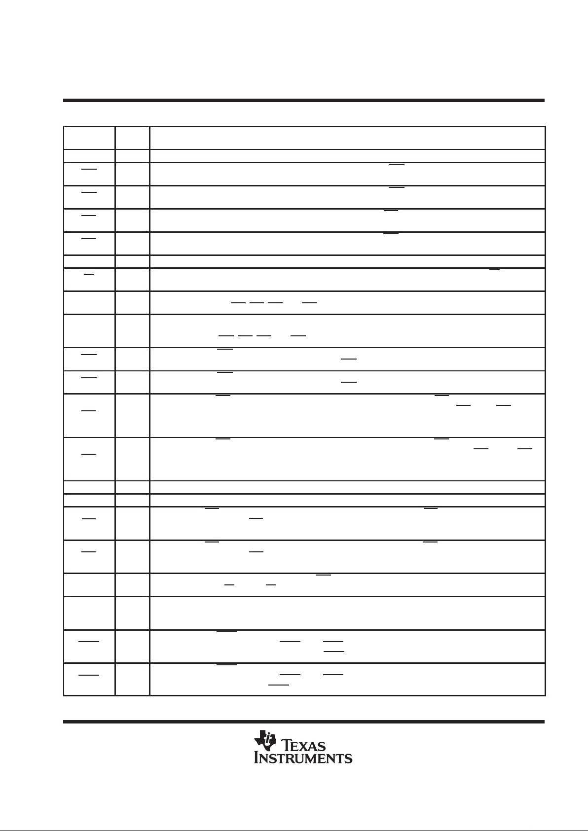
Terminal Functions
TERMINAL
NAME
I/O DESCRIPTION
A0–A35 I/O Port-A data. The 36-bit bidirectional data port for side A.
AEA
O
(port A)
Port-A almost-empty flag. Programmable flag synchronized to CLKA. AEA is low when the number of 36-bit words
in FIFO2 is less than or equal to the value in offset register X.
AEB
O
(port B)
Port-B almost-empty flag. Programmable flag synchronized to CLKB. AEB is low when the number of 36-bit words
in FIFO1 is less than or equal to the value in offset register X.
AFA
O
(port A)
Port-A almost-full flag. Programmable flag synchronized to CLKA. AFA is low when the number of 36-bit empty
locations in FIFO1 is less than or equal to the value in offset register X.
AFB
O
(port B)
Port-B almost-full flag. Programmable flag synchronized to CLKB. AFB is low when the number of 36-bit empty
locations in FIFO2 is less than or equal to the value in offset register X.
B0–B35 I/O Port-B data. The 36-bit bidirectional data port for side B.
BE I
Big-endian select. Selects the bytes on port B used during byte or word data transfer. A low on BE selects the
most-significant bytes on B0–B35 for use, and a high selects the least-significant bytes.
CLKA I
Port-A clock. CLKA is a continuous clock that synchronizes all data transfers through port A and can be asynchronous
or coincident to CLKB. EFA
, FFA, AFA, and AEA are synchronized to the low-to-high transition of CLKA.
CLKB I
Port-B clock. CLKB is a continuous clock that synchronizes all data transfers through port B and can be asynchronous
or coincident to CLKA. Port-B byte swapping and data-port-sizing operations are also synchronous to the low-to-high
transition of CLKB. EFB
, FFB, AFB, and AEB are synchronized to the low-to-high transition of CLKB.
CSA I
Port-A chip select. CSA must be low to enable a low-to-high transition of CLKA to read or write data on port A. The
A0–A35 outputs are in the high-impedance state when CSA
is high.
CSB I
Port-B chip select. CSB must be low to enable a low-to-high transition of CLKB to read or write data on port B. The
B0–B35 outputs are in the high-impedance state when CSB
is high.
EFA
O
(port A)
Port-A empty flag. EFA is synchronized to the low-to-high transition of CLKA. When EFA is low, FIFO2 is empty and
reads from its memory are disabled. Data can be read from FIFO2 to the output register when EFA
is high. EFA is forced
low when the device is reset and is set high by the second low-to-high transition of CLKA after data is loaded into empty
FIFO2 memory.
EFB
O
(port B)
Port-B empty flag. EFB is synchronized to the low-to-high transition of CLKB. When EFB is low, FIFO1 is empty and
reads from its memory are disabled. Data can be read from FIFO1 to the output register when EFB
is high. EFB is
forced low when the device is reset and is set high by the second low-to-high transition of CLKB after data is loaded
into empty FIFO1 memory.
ENA I Port-A enable. ENA must be high to enable a low-to-high transition of CLKA to read or write data on port A.
ENB I Port-B enable. ENB must be high to enable a low-to-high transition of CLKB to read or write data on port B.
FFA
O
(port A)
Port-A full flag. FFA is synchronized to the low-to-high transition of CLKA. When FFA is low, FIFO1 is full and writes
to its memory are disabled. FFA
is forced low when the device is reset and is set high by the second low-to-high
transition of CLKA after reset.
FFB
O
(port B)
Port-B full flag. FFB is synchronized to the low-to-high transition of CLKB. When FFB is low, FIFO2 is full and writes
to its memory are disabled. FFB
is forced low when the device is reset and is set high by the second low-to-high
transition of CLKB after reset.
FS1, FS0 I
Flag offset selects. The low-to-high transition of RST latches the values of FS0 and FS1, which selects one of four
preset values for the AE
flag and AF flag offset.
MBA I
Port-A mailbox select. A high level on MBA chooses a mailbox register for a port-A read or write operation. When the
A0–A35 outputs are active, a high level on MBA selects data from the mail2 register for output and a low level selects
FIFO2 output register data for output.
MBF1 O
Mail1 register flag. MBF1 is set low by the low-to-high transition of CLKA that writes data to the mail1 register. W rites
to the mail1 register are inhibited while MBF1
is low. MBF1 is set high by a low-to-high transition of CLKB when a port-B
read is selected and both SIZ1 and SIZ0 are high. MBF1
is set high when the device is reset.
MBF2 O
Mail2 register flag. MBF2 is set low by the low-to-high transition of CLKB that writes data to the mail2 register. W rites
to the mail2 register are inhibited while MBF2
is low. MBF2 is set high by a low-to-high transition of CLKA when a port-A
read is selected and MBA is high. MBF2
is set high when the device is reset.
SN74ABT3614
64 × 36 × 2 CLOCKED BIDIRECTIONAL FIRST-IN, FIRST-OUT MEMORY
WITH BUS MATCHING AND BYTE SWAPPING
SCBS126H – JUNE 1992 – REVISED APRIL 2000
6
POST OFFICE BOX 655303 • DALLAS, TEXAS 75265
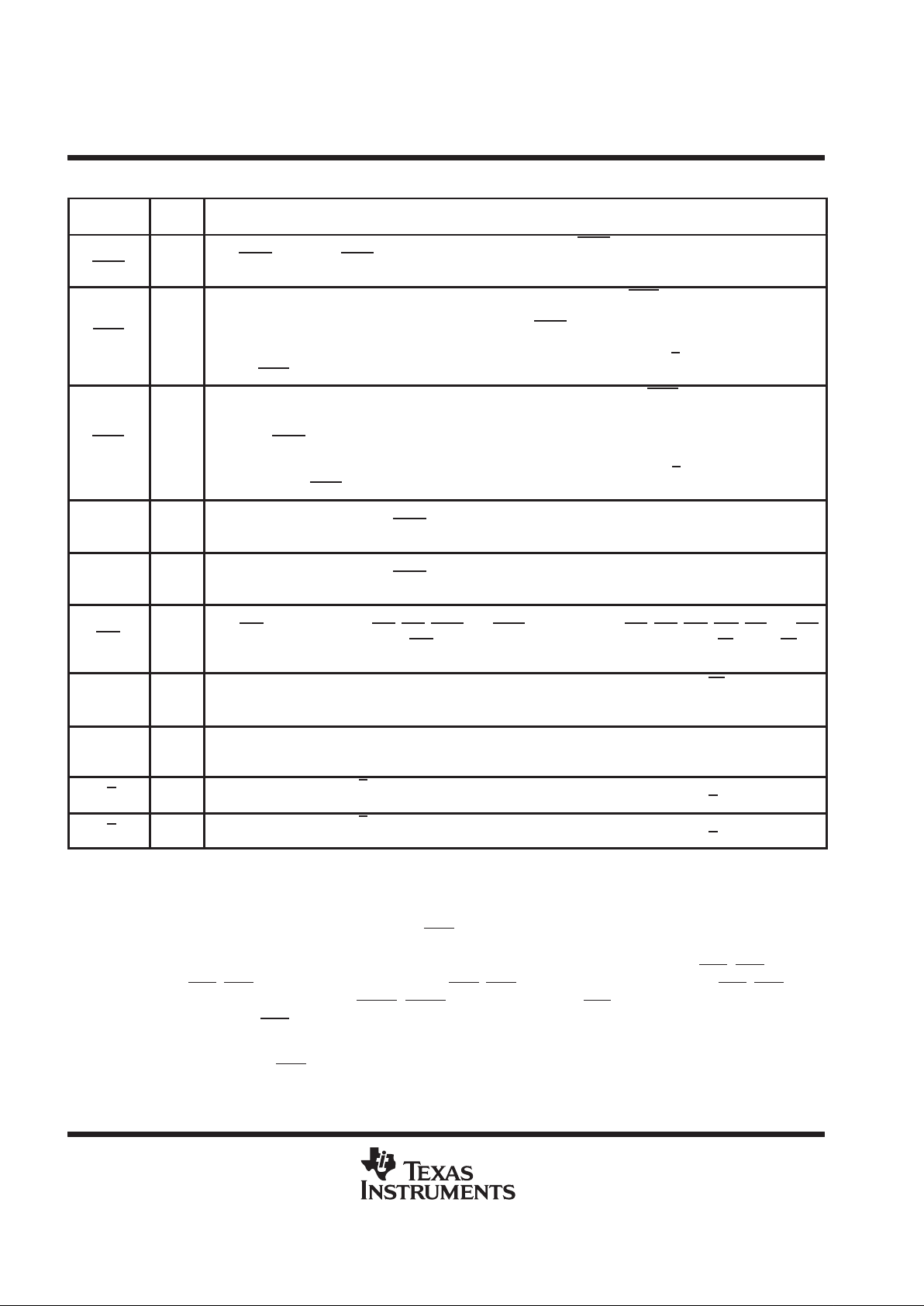
Terminal Functions (Continued)
TERMINAL
NAME
I/O DESCRIPTION
ODD/
EVEN
I
Odd/even parity select. Odd parity is checked on each port when ODD/EVEN is high and even parity is checked when
ODD/EVEN
is low. ODD/EVEN also selects the type of parity generated for each port if parity generation is enabled
for a read operation.
PEFA
O
(port A)
Port-A parity-error flag. When any byte applied to terminals A0–A35 fails parity, PEF A is low . Bytes are organized as
A0–A8, A9–A17, A18–A26, and A27–A35, with the most-significant bit of each byte serving as the parity bit. The
type of parity checked is determined by the state of the ODD/EVEN
input.
The parity trees used to check the A0–A35 inputs are shared by the mail2 register to generate parity if parity generation
is selected by PGA; therefore, if a mail2 read with parity generation is set up by having W/R
A low, MBA high, and PGA
high, the PEFA
flag is forced high, regardless of the state of the A0–A35 inputs.
PEFB
O
(port B)
Port-B parity-error flag. When any valid byte applied to terminals B0–B35 fails parity, PEFB is low . Bytes are organized
as B0–B8, B9–B17, B18–B26, and B27–B35, with the most-significant bit of each byte serving as the parity bit. A
byte is valid when it is used by the bus size selected for port B. The type of parity checked is determined by the state
of the ODD/EVEN
input.
The parity trees used to check the B0–B35 inputs are shared by the mail1 register to generate parity if parity generation
is selected by PGB; therefore, if a mail1 read with parity generation is set up by having W/R
B low, SIZ1 and SIZ0 high,
and PGB high, the PEFB
flag is forced high, regardless of the state of the B0–B35 inputs.
PGA I
Port-A parity generation. Parity is generated for data reads from port A when PGA is high. The type of parity generated
is selected by the state of the ODD/EVEN
input. Bytes are organized as A0–A8, A9–A17, A18–A26, and A27–A35.
The generated parity bits are output in the most-significant bit of each byte.
PGB I
Port-B parity generation. Parity is generated for data reads from port B when PGB is high. The type of parity generated
is selected by the state of the ODD/EVEN
input. Bytes are organized as B0–B8, B9–B17, B18–B26, and B27–B35.
The generated parity bits are output in the most-significant bit of each byte.
RST I
Reset. To reset the device, four low-to-high transitions of CLKA and four low-to-high transitions of CLKB must occur
while RST
is low. This sets the AF A, AFB, MBF1, and MBF2 flags high and the EFA, EFB, AEA, AEB, FFA, and FFB
flags low. The low-to-high transition of RST latches the status of the FS1 and FS0 inputs to select AF flag and AE flag
offset.
SIZ0, SIZ1
I
(port B)
Port-B bus-size selects. The low-to-high transition of CLKB latches the states of SIZ0, SIZ1, and BE, and the following
low-to-high transition of CLKB implements the latched states as a port-B bus size. Port-B bus sizes can be long word,
word, or byte. A high on both SIZ0 and SIZ1 accesses the mailbox registers for a port-B 36-bit write or read.
SW0, SW1
I
(port B)
Port-B byte-swap selects. At the beginning of each long word transfer, one of four modes of byte-order swapping is
selected by SW0 and SW1. The four modes are no swap, byte swap, word swap, and byte-word swap. Byte-order
swapping is possible with any bus-size selection.
W/RA I
Port-A write/read select. W/RA high selects a write operation and a low selects a read operation on port A for a
low-to-high transition of CLKA. The A0–A35 outputs are in the high-impedance state when W/R
A is high.
W/RB I
Port-B write/read select. W/RB high selects a write operation and a low selects a read operation on port B for a
low-to-high transition of CLKB. The B0–B35 outputs are in the high-impedance state when W/R
B is high.
detailed description
reset
The SN74ABT3614 is reset by taking the reset (RST) input low for at least four port-A clock (CLKA) and four
port-B clock (CLKB) low-to-high transitions. The reset input can switch asynchronously to the clocks. A device
reset initializes the internal read and write pointers of each FIFO and forces the full flags (FFA, FFB) low, the
empty flags (EFA, EFB) low , the almost-empty flags (AEA, AEB) low , and the almost-full flags (AF A, AFB) high.
A reset also forces the mailbox flags (MBF1, MBF2) high. After a reset, FFA is set high after two low-to-high
transitions of CLKA and FFB
is set high after two low-to-high transitions of CLKB. The device must be reset after
power up before data is written to its memory.
A low-to-high transition on RST loads the almost-full and almost-empty offset register (X) with the value selected
by the flag-select (FS0, FS1) inputs. The values that can be loaded into the register are shown in Table 1.
SN74ABT3614
64 × 36 × 2 CLOCKED BIDIRECTIONAL FIRST-IN, FIRST-OUT MEMORY
WITH BUS MATCHING AND BYTE SWAPPING
SCBS126H – JUNE 1992 – REVISED APRIL 2000
7
POST OFFICE BOX 655303 • DALLAS, TEXAS 75265
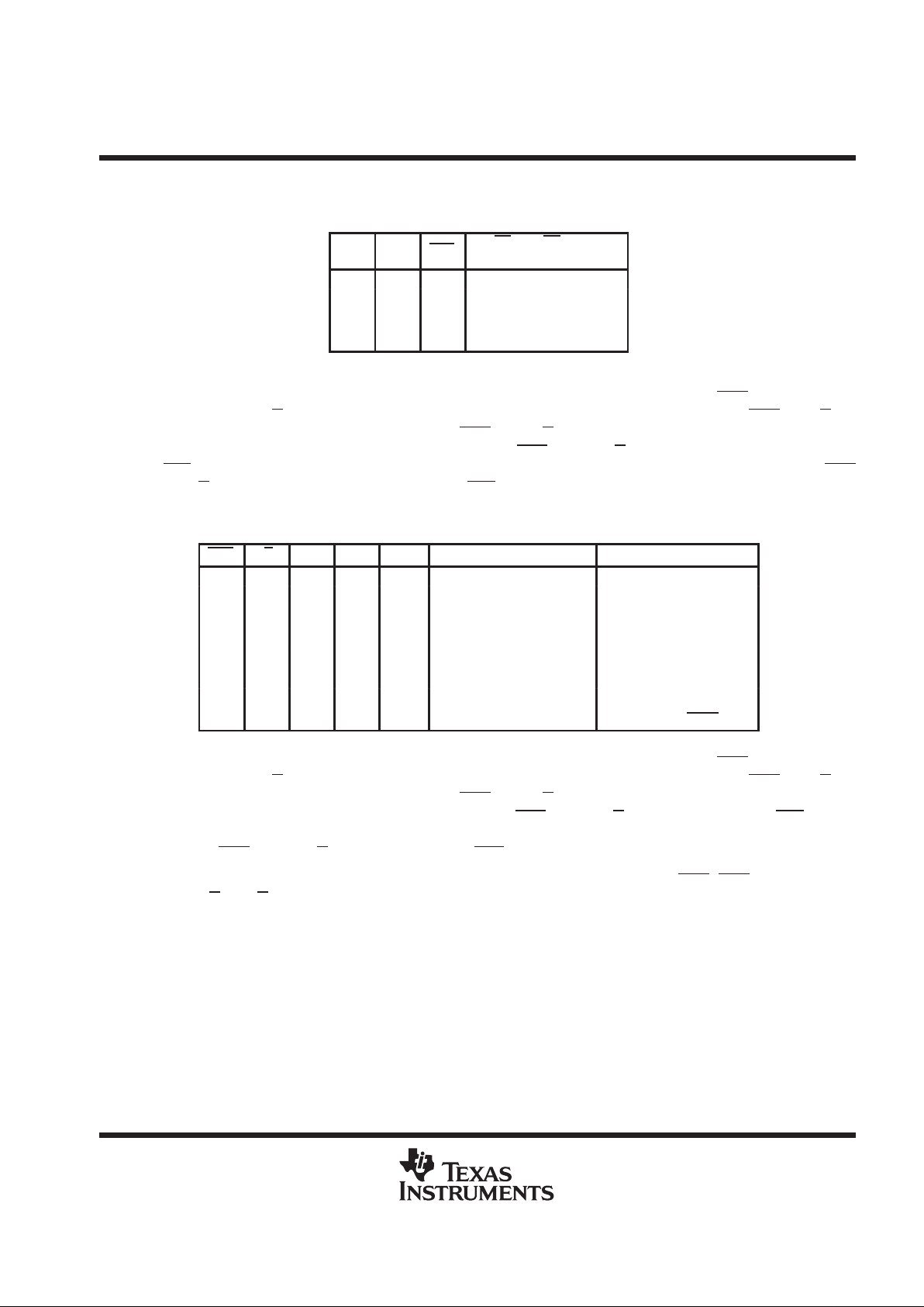
reset (continued)
T able 1. Flag Programming
FS1 FS0
RST
AF AND AE FLAG
OFFSET REGISTER (X)
H H ↑ 16
H L ↑ 12
L H ↑ 8
L L ↑ 4
FIFO write/read operation
The state of the port-A data (A0 –A35) outputs is controlled by the port-A chip select (CSA) and the port-A
write/read select (W/RA). The A0–A35 outputs are in the high-impedance state when either CSA or W/RA is
high. The A0–A35 outputs are active when both CSA and W/RA are low. Data is loaded into FIFO1 from the
A0–A35 inputs on a low-to-high transition of CLKA when CSA is low, W/RA is high, ENA is high, MBA is low,
and FFA
is high. Data is read from FIFO2 to the A0–A35 outputs by a low-to-high transition of CLKA when CSA
is low, W/RA is low, ENA is high, MBA is low, and EFA is high (see Table 2).
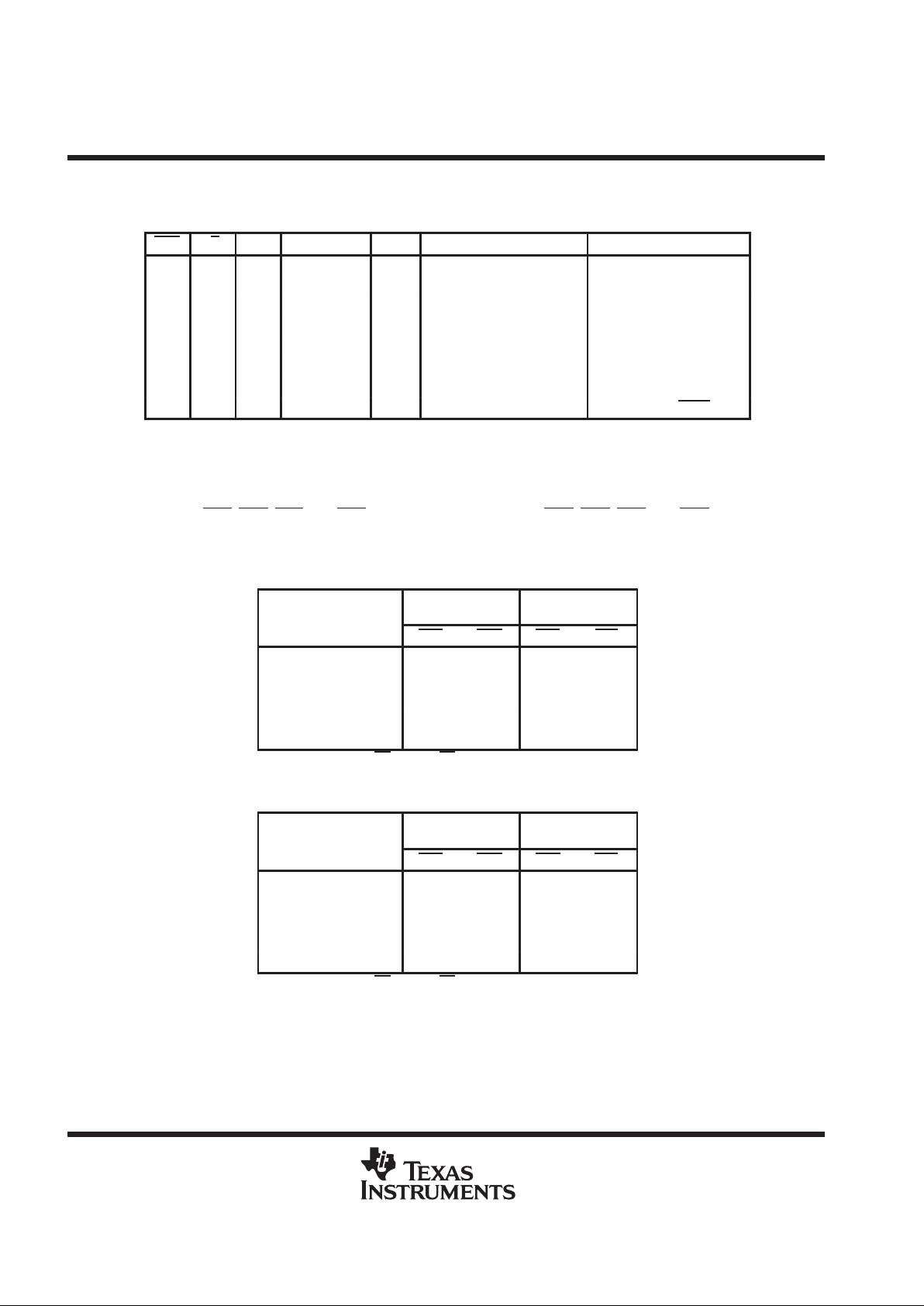
Table 2. Port-A Enable Function Table
CSA W/RA ENA MBA CLKA
A0–A35 OUTPUTS PORT FUNCTION
H X X X X In high-impedance state None
L H L X X In high-impedance state None
L H H L ↑ In high-impedance state FIFO1 write
L H H H ↑ In high-impedance state Mail1 write
L L L L X Active, FIFO2 output register None
L L H L ↑ Active, FIFO2 output register FIFO2 read
L L L H X Active, mail2 register None
L L H H ↑ Active, mail2 register Mail2 read (set MBF2 high)
The state of the port-B data (B0 –B35) outputs is controlled by the port-B chip select (CSB) and the port-B
write/read select (W/RB). The B0–B35 outputs are in the high-impedance state when either CSB or W/RB is
high. The B0–B35 outputs are active when both CSB and W/RB are low. Data is loaded into FIFO2 from the
B0–B35 inputs on a low-to-high transition of CLKB when CSB is low, W/RB is high, ENB is high, FFB is high,
and either SIZ0 or SIZ1 is low. Data is read from FIFO1 to the B0–B35 outputs by a low-to-high transition of
CLKB when CSB
is low, W/RB is low, ENB is high, EFB is high, and either SIZ0 or SIZ1 is low (see Table 3).
The setup- and hold-time constraints to the port clocks for the port-chip selects (CSA
, CSB) and write/read
selects (W/R
A, W/RB) are only for enabling write and read operations and are not related to high-impedance
control of the data outputs. If a port enable is low during a clock cycle, the port-chip select and write/read select
can change states during the setup- and hold-time window of the cycle.
SN74ABT3614
64 × 36 × 2 CLOCKED BIDIRECTIONAL FIRST-IN, FIRST-OUT MEMORY
WITH BUS MATCHING AND BYTE SWAPPING
SCBS126H – JUNE 1992 – REVISED APRIL 2000
8
POST OFFICE BOX 655303 • DALLAS, TEXAS 75265
FIFO writer/read operation (continued)
Table 3. Port-B Enable Function Table
CSB W/RB ENB SIZ1, SIZ0 CLKB
B0–B35 OUTPUTS PORT FUNCTION
H X X X X In high-impedance state None
L H L X X In high-impedance state None
L H H One, both low ↑ In high-impedance state FIFO2 write
L H H Both high ↑ In high-impedance state Mail2 write
L L L One, both low X Active, FIFO1 output register None
L L H One, both low ↑ Active, FIFO1 output register FIFO1 read
L L L Both high X Active, mail1 register None
L L H Both high ↑ Active, mail1 register Mail1 read (set MBF1 high)
synchronized FIFO flags
Each FIFO flag is synchronized to its port clock through two flip-flop stages. This is done to improve flag reliability
by reducing the probability of metastable events on the output when CLKA and CLKB operate asynchronously
to one another. EF A, AEA, FFA, and AF A are synchronized to CLKA. EFB, AEB, FFB, and AFB are synchronized
to CLKB. Tables 4 and 5 show the relationship of each port flag to FIFO1 and FIFO2.
Table 4. FIFO1 Flag Operation
NUMBER OF 36-BIT
SYNCHRONIZED
TO CLKB
SYNCHRONIZED
TO CLKA
WORDS IN FIFO1
†
EFB AEB AFA FFA
0 L L H H
1 to X H LHH
(X + 1) to [64 – (X + 1)] H HHH
(64 – X) to 63 H HLH
64 H H L L
†
X is the value in the AE flag and AF flag offset register.
Table 5. FIFO2 Flag Operation
NUMBER OF 36-BIT
SYNCHRONIZED
TO CLKA
SYNCHRONIZED
TO CLKB
WORDS IN FIFO2
†
EFA AEA AFB FFB
0 L L H H
1 to X H LHH
(X + 1) to [64 – (X + 1)] H HHH
(64 – X) to 63 H HLH
64 H H L L
†
X is the value in the AE flag and AF flag offset register.

SN74ABT3614
64 × 36 × 2 CLOCKED BIDIRECTIONAL FIRST-IN, FIRST-OUT MEMORY
WITH BUS MATCHING AND BYTE SWAPPING
SCBS126H – JUNE 1992 – REVISED APRIL 2000
9
POST OFFICE BOX 655303 • DALLAS, TEXAS 75265
empty flags (EFA, EFB)
The FIFO empty flag is synchronized to the port clock that reads data from its array . When the empty flag is high,
new data can be read to the FIFO output register. When the empty flag is low , the FIFO is empty and attempted
FIFO reads are ignored. When reading FIFO1 with a byte or word size on port B, EFB is set low when the fourth
byte or second word of the last long word is read.
The FIFO read pointer is incremented each time a new word is clocked to the output register. A word written
to a FIFO can be read to the FIFO output register in a minimum of three cycles of the empty-flag synchronizing
clock; therefore, an empty flag is low if a word in memory is the next data to be sent to the FIFO output register
and two cycles of the port clock that reads data from the FIFO have not elapsed since the time the word was
written. The FIFO empty flag is set high by the second low-to-high transition of the synchronizing clock and the
new data word can be read to the FIFO output register in the following cycle.
A low-to-high transition on an empty-flag synchronizing clock begins the first synchronization cycle of a write
if the clock transition occurs at time t
sk1
, or greater, after the write. Otherwise, the subsequent clock cycle can
be the first synchronization cycle (see Figures 13 and 14).
full flags (FFA, FFB)
The FIFO full flag is synchronized to the port clock that writes data to its array. When the full flag is high, a
memory location is free in the SRAM to receive new data. No memory locations are free when the full flag is
low and attempted writes to the FIFO are ignored.
Each time a word is written to a FIFO, the write pointer is incremented. From the time a word is read from a FIFO,
the previous memory location is ready to be written in a minimum of three cycles of the full-flag synchronizing
clock. A full flag is low if less than two cycles of the full-flag synchronizing clock have elapsed since the next
memory write location has been read. The second low-to-high transition on the full-flag synchronizing clock after
the read sets the full flag high and data can be written in the following clock cycle.
A low-to-high transition on a full-flag synchronizing clock begins the first synchronization cycle of a read if the
clock transition occurs at time t
sk1
, or greater, after the read. Otherwise, the subsequent clock cycle can be the
first synchronization cycle (see Figures 15 and 16).
almost-empty flags (AEA, AEB)
The FIFO almost-empty flag is synchronized to the port clock that reads data from its array . The almost-empty
state is defined by the value of the almost-full and almost-empty offset register (X). This register is loaded with
one of four preset values during a device reset (see
reset
). An AE flag is low when the FIFO contains X or fewer
long words in memory and is high when the FIFO contains (X + 1) or more long words.
Two low-to-high transitions of the AE-flag synchronizing clock are required after a FIFO write for the AE flag to
reflect the new level of fill; therefore, the AE flag of a FIFO containing (X + 1) or more long words remains low
if two cycles of the synchronizing clock have not elapsed since the write that filled the memory to the (X + 1)
level. An AE
flag is set high by the second low-to-high transition of the synchronizing clock after the FIFO write
that fills memory to the (X + 1) level. A low-to-high transition of an AE flag synchronizing clock begins the first
synchronization cycle if it occurs at time t
sk2
, or greater, after the write that fills the FIFO to (X + 1) long words.
Otherwise, the subsequent synchronizing clock cycle can be the first synchronization cycle (see Figures 17 and
18).

SN74ABT3614
64 × 36 × 2 CLOCKED BIDIRECTIONAL FIRST-IN, FIRST-OUT MEMORY
WITH BUS MATCHING AND BYTE SWAPPING
SCBS126H – JUNE 1992 – REVISED APRIL 2000
10
POST OFFICE BOX 655303 • DALLAS, TEXAS 75265
almost-full flags (AFA, AFB)
The FIFO almost-full flag is synchronized to the port clock that writes data to its array . The almost-full state is
defined by the value of the almost-full and almost-empty offset register (X). This register is loaded with one of
four preset values during a device reset (see
reset
). An almost-full flag is low when the FIFO contains (64 – X)
or more long words in memory and is high when the FIFO contains [64 – (X + 1)] or fewer long words.
Two low-to-high transitions of the AF
-flag synchronizing clock are required after a FIFO read for the AF flag to
reflect the new level of fill; therefore, the AF flag of a FIFO containing [64 – (X + 1)] or fewer words remains low
if two cycles of the synchronizing clock have not elapsed since the read that reduced the number of long words
in memory to [64 – (X + 1)]. An AF flag is set high by the second low-to-high transition of the synchronizing clock
after the FIFO read that reduces the number of long words in memory to [64 – (X + 1)]. A low-to-high transition
of an AF
-flag synchronizing clock begins the first synchronization cycle if it occurs at time t
sk2
, or greater, after
the read that reduces the number of long words in memory to [64 – (X + 1)]. Otherwise, the subsequent
synchronizing clock cycle can be the first synchronization cycle (see Figures 19 and 20).
mailbox registers
Each FIFO has a 36-bit bypass register to pass command and control information between port A and port B
without putting it in queue. The mailbox-select (MBA, MBB) inputs choose between a mail register and a FIFO
for a port data-transfer operation. A low-to-high transition on CLKA writes A0–A35 data to the mail1 register
when a port-A write is selected by CSA, W/RA, and ENA, and MBA is high. A low-to-high transition on CLKB
writes B0–B35 data to the mail2 register when a port-B write is selected by CSB, W/RB, and ENB and both SIZ0
and SIZ1 are high. Writing data to a mail register sets the corresponding flag (MBF1 or MBF2) low . Attempted
writes to a mail register are ignored while the mail flag is low.
When the port-A data outputs (A0–A35) are active, the data on the bus comes from the FIFO2 output register
when MBA is low and from the mail2 register when MBA is high. When the port-B data outputs (B0–B35) are
active, the data on the bus comes from the FIFO1 output register when either one or both SIZ1 and SIZ0 are
low and from the mail2 register when both SIZ1 and SIZ0 are high. The mail1 register flag (MBF1
) is set high
by a rising CLKB edge when a port-B read is selected by CSB, W/RB, and ENB and both SIZ1 and SIZ0 are
high. The mail2 register flag (MBF2) is set high by a rising CLKA edge when a port-A read is selected by CSA,
W/RA, and ENA and MBA is high. The data in the mail register remains intact after it is read and changes only
when new data is written to the register.
dynamic bus sizing
The port-B bus can be configured in a 36-bit long word, 18-bit word, or 9-bit byte format for data read from FIFO1
or written to FIFO2. Word- and byte-size bus selections can utilize the most-significant bytes of the bus (big
endian) or least-significant bytes of the bus (little endian). Port-B bus size can be changed dynamically and
synchronous to CLKB to communicate with peripherals of various bus widths.
The levels applied to the port-B bus-size select (SIZ0, SIZ1) inputs and the big-endian select (BE) input are
stored on each CLKB low-to-high transition. The stored port-B bus-size selection is implemented by the next
rising edge on CLKB according to Figure 1.
Only 36-bit long-word data is written to or read from the two FIFO memories on the SN74ABT3614.
Bus-matching operations are done after data is read from the FIFO1 RAM and before data is written to the FIFO2
RAM. Port-B bus sizing does not apply to mail-register operations.
SN74ABT3614
64 × 36 × 2 CLOCKED BIDIRECTIONAL FIRST-IN, FIRST-OUT MEMORY
WITH BUS MATCHING AND BYTE SWAPPING
SCBS126H – JUNE 1992 – REVISED APRIL 2000
11
POST OFFICE BOX 655303 • DALLAS, TEXAS 75265
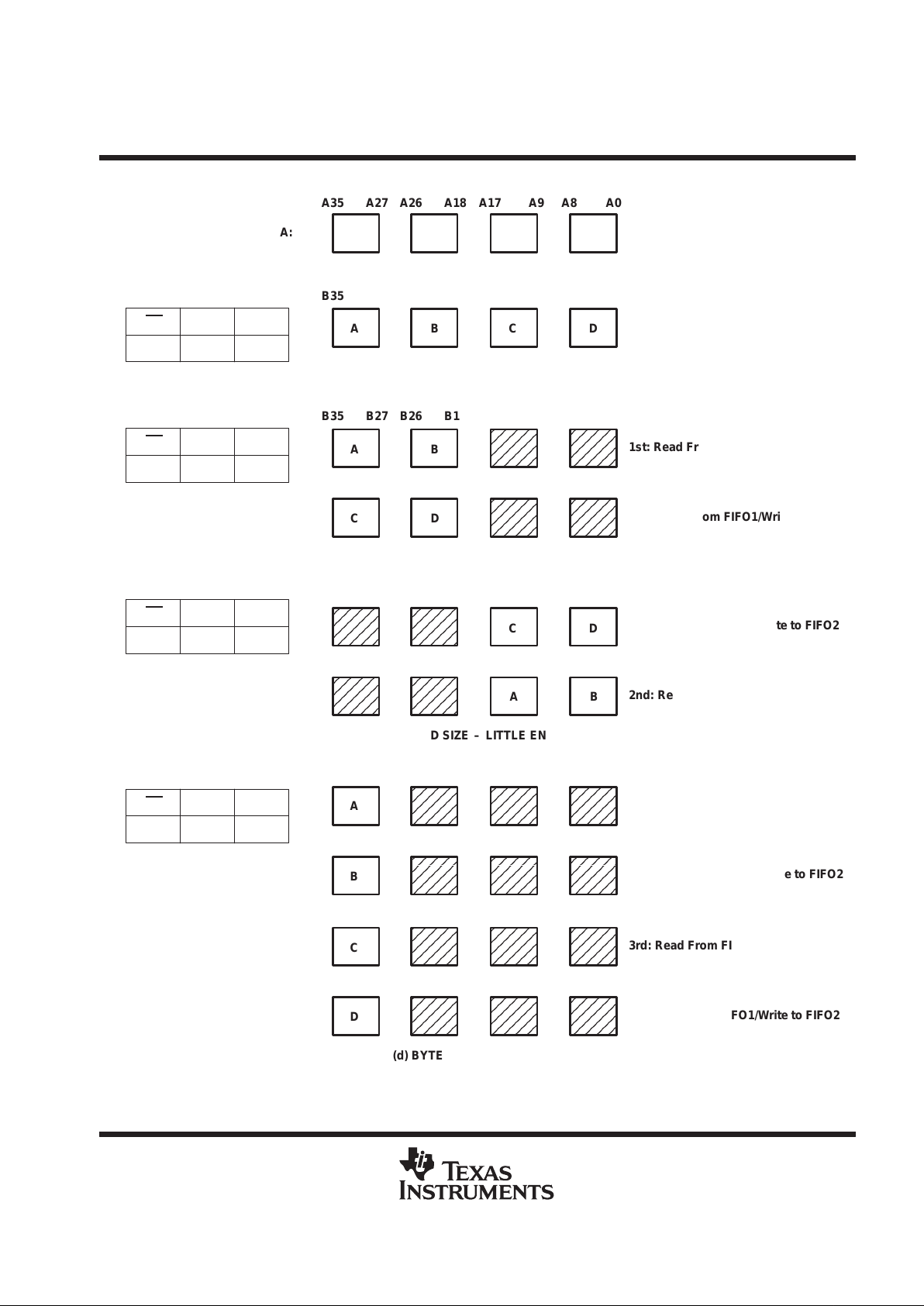
dynamic bus sizing (continued)
Read From FIFO1/Write to FIFO2
Write to FIFO1/Read From FIFO2
(a) LONG WORD SIZE
1st: Read From FIFO1/Write to FIFO2
2nd: Read From FIFO1/Write to FIFO2
(b) WORD SIZE – BIG ENDIAN
1st: Read From FIFO1/Write to FIFO2
2nd: Read From FIFO1/Write to FIFO2
(c) WORD SIZE – LITTLE ENDIAN
1st: Read From FIFO1/Write to FIFO2
2nd: Read From FIFO1/Write to FIFO2
3rd: Read From FIFO1/Write to FIFO2
4th: Read From FIFO1/Write to FIFO2
(d) BYTE SIZE – BIG ENDIAN
BYTE ORDER ON PORT A:
A35 A27 A26 A18 A17 A9 A8 A0
B35 B27 B26 B18 B17 B9 B8 B0
XLL
BE
SIZ1 SIZ0
ABCD
ABCD
AB
CD
CD
AB
A
B
C
D
B35 B27 B26 B18 B17 B9 B8 B0
B35 B27 B26 B18 B17 B9 B8 B0
B35 B27 B26 B18 B17 B9 B8 B0
B35 B27 B26 B18 B17 B9 B8 B0
B35 B27 B26 B18 B17 B9 B8 B0
B35 B27 B26 B18 B17 B9 B8 B0
B35 B27 B26 B18 B17 B9 B8 B0
B35 B27 B26 B18 B17 B9 B8 B0
LLH
BE SIZ1 SIZ0
HLH
BE
SIZ1 SIZ0
LHL
BE SIZ1 SIZ0
Figure 1. Dynamic Bus Sizing
SN74ABT3614
64 × 36 × 2 CLOCKED BIDIRECTIONAL FIRST-IN, FIRST-OUT MEMORY
WITH BUS MATCHING AND BYTE SWAPPING
SCBS126H – JUNE 1992 – REVISED APRIL 2000
12
POST OFFICE BOX 655303 • DALLAS, TEXAS 75265
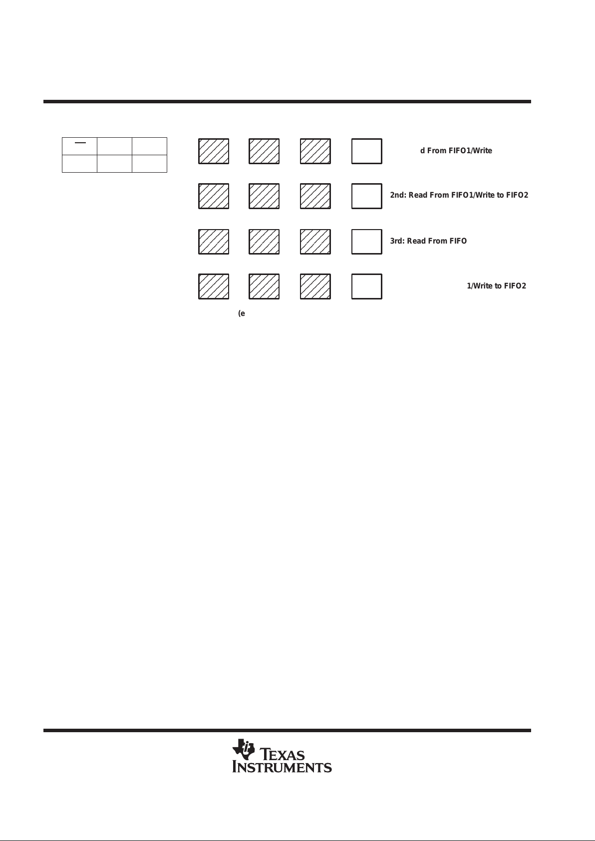
dynamic bus sizing (continued)
2nd: Read From FIFO1/Write to FIFO2
3rd: Read From FIFO1/Write to FIFO2
4th: Read From FIFO1/Write to FIFO2
(e) BYTE SIZE – LITTLE ENDIAN
1st: Read From FIFO1/Write to FIFO2
B35 B27 B26 B18 B17 B9 B8 B0
B35 B27 B26 B18 B17 B9 B8 B0
B35 B27 B26 B18 B17 B9 B8 B0
B35 B27 B26 B18 B17 B9 B8 B0
D
C
B
A
HHL
BE
SIZ1 SIZ0
Figure 1. Dynamic Bus Sizing (continued)
bus-matching FIFO1 reads
Data is read from the FIFO1 RAM in 36-bit long-word increments. If a long-word bus size is implemented, the
entire long word immediately shifts to the FIFO1 output register. If byte or word size is implemented on port B,
only the first one or two bytes appear on the selected portion of the FIFO1 output register with the rest of the
long word stored in auxiliary registers. In this case, subsequent FIFO1 reads with the same bus-size
implementation output the rest of the long word to the FIFO1 output register in the order shown by Figure 1.
Each FIFO1 read with a new bus-size implementation automatically unloads data from the FIFO1 RAM to its
output register and auxiliary registers. Therefore, implementing a new port-B bus size and performing a FIFO1
read before all bytes or words stored in the auxiliary registers have been read results in a loss of the unread
long-word data.
When reading data from FIFO1 in byte or word format, the unused B0–B35 outputs remain inactive but static
with the unused FIFO1 output register bits holding the last data value to decrease power consumption.
bus-matching FIFO2 writes
Data is written to the FIFO2 RAM in 36-bit long-word increments. FIFO2 writes with a long-word bus size
immediately store each long word in FIFO2 RAM. Data written to FIFO2 with a byte or word bus size stores the
initial bytes or words in auxiliary registers. The CLKB rising edge that writes the fourth byte or the second word
of long word to FIFO2 also stores the entire long word in FIFO2 RAM. The bytes are arranged in the manner
shown in Figure 1.
Each FIFO2 write with a new bus-size implementation resets the state machine that controls the data flow from
the auxiliary registers to the FIFO2 RAM. Therefore, implementing a new bus size and performing a FIFO2 write
before bytes or words stored in the auxiliary registers have been loaded to FIFO2 RAM results in a loss of data.
SN74ABT3614
64 × 36 × 2 CLOCKED BIDIRECTIONAL FIRST-IN, FIRST-OUT MEMORY
WITH BUS MATCHING AND BYTE SWAPPING
SCBS126H – JUNE 1992 – REVISED APRIL 2000
13
POST OFFICE BOX 655303 • DALLAS, TEXAS 75265
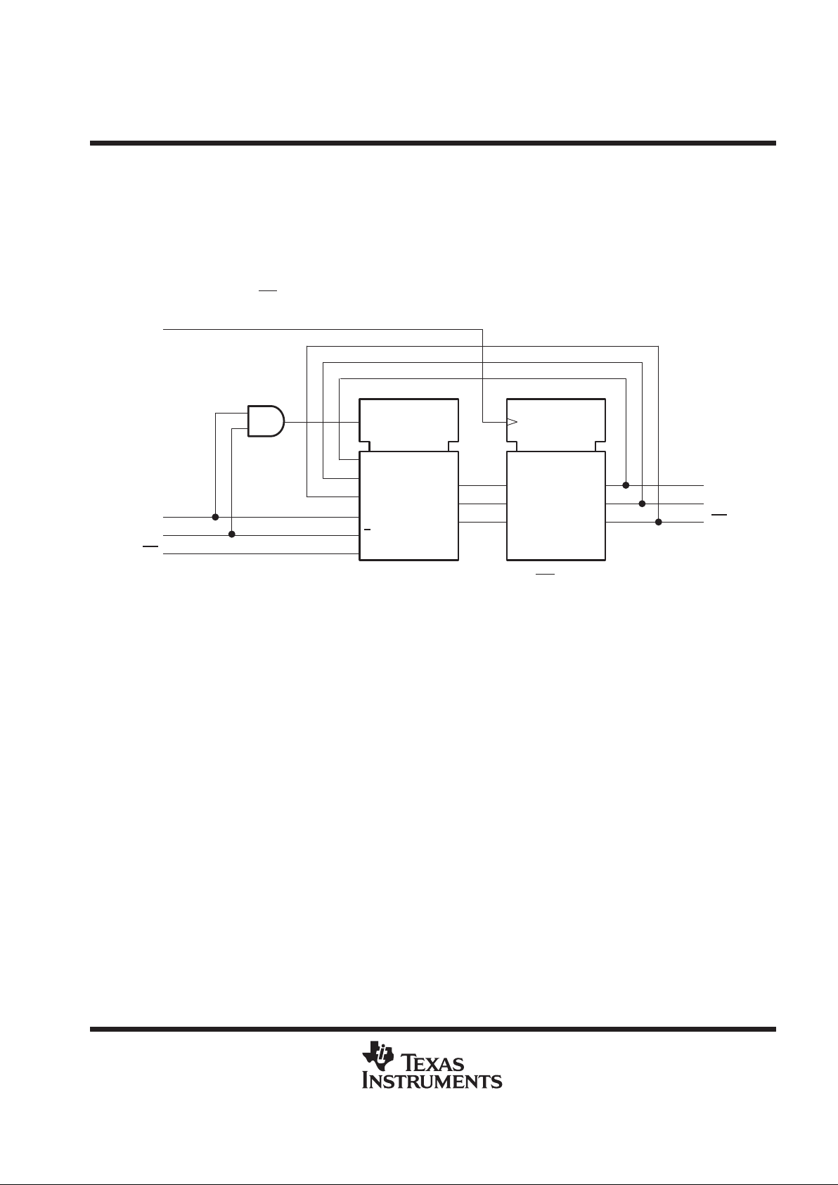
port-B mail-register access
In addition to selecting port-B bus sizes for FIFO reads and writes, the port-B bus size select (SIZ0, SIZ1) inputs
also access the mail registers. When both SIZ0 and SIZ1 are high, the mail1 register is accessed for a port-B
long-word read and the mail2 register is accessed for a port-B long-word write. The mail register is accessed
immediately. Any bus-sizing operation that is underway is unaffected by the mail-register access. After the
mail-register access is complete, the previous FIFO access can resume in the next CLKB cycle. The logic
diagram in Figure 2 shows that the previous bus-size selection is preserved when the mail registers are
accessed from port B. A port-B bus size is implemented on each rising CLKB edge according to the states of
SIZ0_Q, SIZ1_Q, and BE
_Q.
MUX
CLKB
SIZ0
SIZ1
BE
SIZ0_Q
SIZ1_Q
BE
_Q
DQ
G1
1
1
Figure 2. Logic Diagram for SIZ0, SIZ1, and BE Register
byte swapping
The byte-order arrangement of data read from FIFO1 or data written to FIFO2 can be changed synchronous
to the rising edge of CLKB. Byte-order swapping is not available for mail-register data. Four modes of byte-order
swapping (including no swap) can be done with any data-port-size selection. The order of the bytes is
rearranged within the long word, but the bit order within the bytes remains constant.
Byte arrangement is chosen by the port-B swap select (SW0, SW1) inputs on a CLKB rising edge that reads
a new long word from FIFO1 or writes a new long word to FIFO2. The byte order chosen on the first byte or first
word of a new long-word read from FIFO1 or written to FIFO2 is maintained until the entire long word is
transferred, regardless of the SW0 and SW1 states during subsequent writes or reads. Figure 3 is an example
of the byte-order swapping available for long words. Performing a byte swap and bus size simultaneously for
a FIFO1 read first rearranges the bytes as shown in Figure 3, then outputs the bytes as shown in Figure 1.
Simultaneous bus-sizing and byte-swapping operations for FIFO2 writes load the data according to Figure 1,
then swap the bytes as shown in Figure 3 when the long word is loaded to FIFO2 RAM.

SN74ABT3614
64 × 36 × 2 CLOCKED BIDIRECTIONAL FIRST-IN, FIRST-OUT MEMORY
WITH BUS MATCHING AND BYTE SWAPPING
SCBS126H – JUNE 1992 – REVISED APRIL 2000
14
POST OFFICE BOX 655303 • DALLAS, TEXAS 75265
byte swapping (continued)
(a) NO SWAP
(b) BYTE SWAP
(c) WORD SWAP
(d) BYTE-WORD SWAP
LL
SW1 SW0
LH
SW1 SW0
HL
SW1 SW0
HH
SW1 SW0
A35 A27 A26 A18 A17 A9 A8 A0
AB CD
AB CD
AB CD
AB CD
AB CD
DC BA
CD AB
BA DC
B35 B27 B26 B18 B17 B9 B8 B0
A35 A27 A26 A18 A17 A9 A8 A0
B35 B27 B26 B18 B17 B9 B8 B0
A35 A27 A26 A18 A17 A9 A8 A0
B35 B27 B26 B18 B17 B9 B8 B0
A35 A27 A26 A18 A17 A9 A8 A0
B35 B27 B26 B18 B17 B9 B8 B0
Figure 3. Byte Swapping (Long-Word Size Example)

SN74ABT3614
64 × 36 × 2 CLOCKED BIDIRECTIONAL FIRST-IN, FIRST-OUT MEMORY
WITH BUS MATCHING AND BYTE SWAPPING
SCBS126H – JUNE 1992 – REVISED APRIL 2000
15
POST OFFICE BOX 655303 • DALLAS, TEXAS 75265
parity checking
The port-A data inputs (A0–A35) and port-B data inputs (B0–B35) each have four parity trees to check the parity
of incoming (or outgoing) data. A parity failure on one or more bytes of the port-A data bus is reported by a low
level on the port-A parity error flag (PEFA). A parity failure on one or more bytes of the port-B data inputs that
are valid for the bus-size implementation is reported by a low level on the port-B parity-error flag (PEFB). Oddor even-parity checking can be selected, and the parity-error flags can be ignored if this feature is not desired.
Parity status is checked on each input bus according to the level of the odd/even parity (ODD/EVEN) select
input. A parity error on one or more valid bytes of a port is reported by a low level on the corresponding
port-parity-error flag (PEFA, PEFB) output. Port-A bytes are arranged as A0–A8, A9–A17, A18–A26, and
A27–A35. Port-B bytes are arranged as B0–B8, B9–B17, B18–B26, and B27–B35, and its valid bytes are
those used in a port-B bus-size implementation. When odd/even parity is selected, a port parity-error flag
(PEFA
, PEFB) is low if any valid byte on the port has an odd/even number of low levels applied to the bits.
The four parity trees used to check the A0–A35 inputs are shared by the mail2 register when parity generation
is selected for port-A reads (PGA = high). When a port-A read from the mail2 register with parity generation is
selected with CSA low, ENA high, W/RA low, MBA high, and PGA high, the port-A parity-error flag (PEFA) is
held high, regardless of the levels applied to the A0 – A35 inputs. Likewise, the parity trees used to check
the B0 –B35 inputs are shared by the mail1 register when parity generation is selected for port-B reads
(PGB = high). When a port-B read from the mail1 register with parity generation is selected with CSB low , ENB
high, and W/R
B low, both SIZ0 and SIZ1 high, and PGB high, the port-B parity-error flag (PEFB) is held high,
regardless of the levels applied to the B0–B35 inputs.
parity generation
A high level on the port-A parity-generate select (PGA) or port-B parity-generate select (PGB) enables the
SN74ABT3614 to generate parity bits for port reads from a FIFO or mailbox register . Port-A bytes are arranged
as A0–A8, A9–A17, A18–A26, and A27–A35, with the most-significant bit of each byte used as the parity bit.
Port-B bytes are arranged as B0–B8, B9–B17, B18–B26, and B27–B35, with the most-significant bit of each
byte used as the parity bit. A write to a FIFO or mail register stores the levels applied to all nine inputs of a byte,
regardless of the state of the parity-generate select (PGA, PGB) inputs. When data is read from a port with parity
generation selected, the lower eight bits of each byte are used to generate a parity bit according to the level on
the ODD/EVEN
select. The generated parity bits are substituted for the levels originally written to the
most-significant bits of each byte as the word is read to the data outputs.
Parity bits for FIFO data are generated after the data is read from SRAM and before the data is written to the
output register. The port-A parity-generate select (PGA) and odd/even parity select (ODD/EVEN) have setupand hold-time constraints to the port-A clock (CLKA) and the port-B parity generate select (PGB) and
ODD/EVEN have setup- and hold-time constraints to the port-B clock (CLKB). These timing constraints apply
only for a rising clock edge used to read a new long word to the FIFO output register.
The circuit used to generate parity for the mail1 data is shared by the port-B bus (B0–B35) to check parity . The
circuit used to generate parity for the mail2 data is shared by the port-A bus (A0 –A35) to check parity. The
shared parity trees of a port are used to generate parity bits for the data in a mail register when the port chip
select (CSA
, CSB) is low, enable (ENA, ENB) is high, write/read select (W/RA, W/RB) input is low, the mail
register is selected (MBA is high for port A; both SIZ0 and SIZ1 are high for port B), and port parity-generate
select (PGA, PGB) is high. Generating parity for mail register data does not change the contents of the register.

SN74ABT3614
64 × 36 × 2 CLOCKED BIDIRECTIONAL FIRST-IN, FIRST-OUT MEMORY
WITH BUS MATCHING AND BYTE SWAPPING
SCBS126H – JUNE 1992 – REVISED APRIL 2000
16
POST OFFICE BOX 655303 • DALLAS, TEXAS 75265
t
pd(C-AF)
CLKA
CLKB
RST
0,1
t
h(FS)
t
su(FS)
t
h(RS)
t
su(RS)
FS1, FS0
FFA
t
pd(C-FF)
t
pd(C-FF)
EFA
t
pd(C-EF)
t
pd(C-AE)
AEA
AFA
MBF1,
MBF2
t
pd(R-F)
t
pd(C-FF)
t
pd(C-FF)
FFB
EFB
t
pd(C-AF)
t
pd(C-AE)
AEB
AFB
t
pd(C-EF)
Figure 4. Device Reset Loading the X Register With the Value of Eight

SN74ABT3614
64 × 36 × 2 CLOCKED BIDIRECTIONAL FIRST-IN, FIRST-OUT MEMORY
WITH BUS MATCHING AND BYTE SWAPPING
SCBS126H – JUNE 1992 – REVISED APRIL 2000
17
POST OFFICE BOX 655303 • DALLAS, TEXAS 75265
t
su(D)
CLKA
FFA
CSA
W2
†
t
su(EN)
t
w(CLKL)
t
c
t
w(CLKH)
t
h(EN)
t
h(EN)
t
su(EN)
t
su(EN)
ППППППП
W/RA
MBA
ENA
A0–A35
W1
†
ООООООО
t
su(EN)
t
h(EN)
t
su(EN)
t
h(EN)
t
su(EN)
t
h(EN)
t
h(D)
t
h(EN)
No Operation
ODD/
EVEN
Valid
PEFA
Valid
t
pd(D-PE)
t
pd(D-PE)
High
†
Written to FIFO1
Figure 5. Port-A Write-Cycle Timing for FIFO1

SN74ABT3614
64 × 36 × 2 CLOCKED BIDIRECTIONAL FIRST-IN, FIRST-OUT MEMORY
WITH BUS MATCHING AND BYTE SWAPPING
SCBS126H – JUNE 1992 – REVISED APRIL 2000
18
POST OFFICE BOX 655303 • DALLAS, TEXAS 75265
SIZ1,
SIZ0
t
su(EN)
W/RB
CLKB
FFB
CSB
t
su(EN)
ENB
B0–B35
t
su(EN)
t
su(EN)
t
h(EN)
t
su(D)
t
h(D)
t
h(EN)
ODD/
EVEN
Valid
PEFB
Valid
t
pd(C-PE)
t
pd(D-PE)
High
SW1,
SW0
t
su(SW)
t
h(SW)
(0, 0)
Not (1, 1)
†
(0, 0)
t
su(SZ)
t
h(SZ)
BE
t
h(SZ)
t
su(SZ)
†
SIZ0 = H and SIZ1 = H writes data to the mail2 register.
DATA SWAP TABLE FOR LONG-WORD WRITES TO FIFO2
SWAP MODE
DATA WRITTEN TO FIFO2 DATA READ FROM FIFO2
SW1 SW0
B35–B27 B26–B18 B17–B9 B8–B0 A35–A27 A26–A18 A17–A9 A8–A0
L L A B C D A B C D
L HD CBAA BCD
H LC DABA BCD
H H B A D C A B C D
Figure 6. Port-B Long-Word Write-Cycle Timing for FIFO2

SN74ABT3614
64 × 36 × 2 CLOCKED BIDIRECTIONAL FIRST-IN, FIRST-OUT MEMORY
WITH BUS MATCHING AND BYTE SWAPPING
SCBS126H – JUNE 1992 – REVISED APRIL 2000
19
POST OFFICE BOX 655303 • DALLAS, TEXAS 75265
SIZ1, SIZ0
W/RB
CLKB
FFB
CSB
ENB
(0, 1)
(0, 1) Not (1, 1)
†
BE
B0–B17
B18–B35
Little
Endian
Big
Endian
ODD/EVEN
PEFB
Valid Valid
t
pd(C-PE)
t
pd(D-PE)
SW1, SW0
High
t
su(D)
t
h(D)
t
su(D)
t
h(D)
t
su(SZ)
t
h(SZ)
t
su(SZ)
t
h(SZ)
t
su(SW)
t
h(SW)
t
su(EN)
t
h(EN)tsu(EN)
t
h(EN)
t
su(EN)
t
su(EN)
t
h(EN)
t
su(SZ)
t
h(SZ)
t
su(SZ)
t
h(SZ)
†
SIZ0 = H and SIZ1 = H writes data to the mail2 register.
NOTE A: PEFB
indicates parity error for the following bytes: B35–B27 and B26–B18 for big-endian bus, and B17–B9 and B8–B0 for little-
endian bus.
DATA SWAP TABLE FOR WORD WRITES TO FIFO2
DATA WRITTEN TO FIFO2
SWAP MODE
WRITE
BIG ENDIAN LITTLE ENDIAN
DATA READ FROM FIFO2
SW1 SW0
NO
.
B35–B27 B26–B18 B17–B9 B8–B0 A35–A27 A26–A18 A17–A9 A8–A0
L L
1
2
A
C
B
D
C
A
D
B
A B C D
L H
1
2
D
B
C
A
B
D
A
C
A B C D
H L
1
2
C
A
D
B
A
C
B
D
A B C D
H H
1
2
B
D
A
C
D
B
C
A
A B C D
Figure 7. Port-B Word Write-Cycle Timing for FIFO2

SN74ABT3614
64 × 36 × 2 CLOCKED BIDIRECTIONAL FIRST-IN, FIRST-OUT MEMORY
WITH BUS MATCHING AND BYTE SWAPPING
SCBS126H – JUNE 1992 – REVISED APRIL 2000
20
POST OFFICE BOX 655303 • DALLAS, TEXAS 75265
t
pd(C-PE)
t
pd(D-PE)
SIZ1, SIZ0
W/R
B
CLKB
FFB
CSB
ENB
BE
B0–B8
B27–B35
Little
Endian
Big
Endian
ODD/EVEN
PEFB Valid
SW1, SW0
ÌÌÌ
Valid
Valid
Valid
t
pd(D-PE)
t
pd(D-PE)
t
su(D)
t
h(D)
(1, 0) (1, 0) (1, 0)
Not (1, 1)
†
(1, 0)
t
su(D)
t
h(D)
t
su(SZ)
t
h(SZ)
t
su(SZ)
t
h(SZ)
t
su(SZ)
t
h(SZ)
t
su(SZ)
t
h(SZ)
t
su(SW)
t
h(EN)
t
su(EN)
t
h(EN)
t
su(EN)
t
h(EN)
High
t
su(EN)
t
su(EN)
t
h(EN)
†
SIZ0 = H and SIZ1 = H writes data to the mail2 register.
NOTE A: PEFB
indicates parity error for the following bytes: B35–B27 for big-endian bus and B17–B9 for little-endian bus.
Figure 8. Port-B Byte Write-Cycle Timing for FIFO2

SN74ABT3614
64 × 36 × 2 CLOCKED BIDIRECTIONAL FIRST-IN, FIRST-OUT MEMORY
WITH BUS MATCHING AND BYTE SWAPPING
SCBS126H – JUNE 1992 – REVISED APRIL 2000
21
POST OFFICE BOX 655303 • DALLAS, TEXAS 75265
DATA SWAP TABLE FOR BYTE WRITES TO FIFO2
DATA WRITTEN
TO FIFO2
SWAP MODE
WRITE
NO.
BIG
ENDIAN
LITTLE
ENDIAN
DATA READ FROM FIFO2
SW1 SW0
B35–B27 B8–B0 A35– A27 A26–A18 A17–A9 A8–A0
L L
1
2
3
4
A
B
C
D
D
C
B
A
A B C D
L H
1
2
3
4
D
C
B
A
A
B
C
D
A B C D
H L
1
2
3
4
C
D
A
B
B
A
D
C
A B C D
H H
1
2
3
4
B
A
D
C
C
D
A
B
A B C D
Figure 8. Port-B Byte Write-Cycle Timing for FIFO2 (Continued)

SN74ABT3614
64 × 36 × 2 CLOCKED BIDIRECTIONAL FIRST-IN, FIRST-OUT MEMORY
WITH BUS MATCHING AND BYTE SWAPPING
SCBS126H – JUNE 1992 – REVISED APRIL 2000
22
POST OFFICE BOX 655303 • DALLAS, TEXAS 75265
SIZ1,
SIZ0
W/RB
CLKB
EFB
CSB
ENB
B0–B35
t
su(EN)
t
h(EN)
PGB,
ODD/
EVEN
High
SW1,
SW0
t
su(SW)
t
h(SW)
(0, 0) Not (1, 1)
†
(0, 0)
t
su(SZ)
t
h(SZ)
BE
t
h(SZ)
t
su(SZ)
t
su(EN)
t
h(EN)
Not (1, 1)
†
t
h(PG)
t
en
Previous Data
W1
‡
W2
‡
t
a
t
a
t
dis
No Operation
t
su(PG)
†
SIZ0 = H and SIZ1 = H selects the mail1 register for output on B0–B35.
‡
Data read from FIFO1
DATA SWAP TABLE FOR LONG-WORD READS FROM FIFO1
DATA WRITTEN TO FIFO1
SWAP MODE DATA READ FROM FIFO1
A35–A27 A26–A18 A17–A9 A8–A0
SW1 SW0
B35–B27 B26–B18 B17–B9 B8–B0
A B C D L L A B C D
A BCDLHD CBA
A BCDHLC DAB
A B C D H H B A D C
Figure 9. Port-B Long-Word Read-Cycle Timing for FIFO1

SN74ABT3614
64 × 36 × 2 CLOCKED BIDIRECTIONAL FIRST-IN, FIRST-OUT MEMORY
WITH BUS MATCHING AND BYTE SWAPPING
SCBS126H – JUNE 1992 – REVISED APRIL 2000
23
POST OFFICE BOX 655303 • DALLAS, TEXAS 75265
ÎÎÎÎ
SIZ1,
SIZ0
W/RB
CLKB
EFB
CSB
ENB
B0–B17
t
su(EN)
t
h(EN)
PGB,
ODD/
EVEN
High
SW1,
SW0
t
su(SW)
t
h(SW)
(0, 1) Not (1, 1)
†
(0, 1)
t
su(SZ)
t
h(SZ)
BE
t
h(SZ)
t
su(SZ)
Not (1, 1)
†
t
su(PG)
t
h(PG)
t
en
Previous Data Read 1 Read 2
t
a
t
a
t
dis
No Operation
Little
Endian
‡
Big
Endian
‡
B18–B35
Previous Data Read 1 Read 2
t
a
t
a
t
dis
†
SIZ0 = H and SIZ1 = H selects the mail1 register for output on B0–B35.
‡
Unused word B0–B17 or B18–B35 holds the last FIFO1-output-register data for word-size reads.
DATA SWAP TABLE FOR WORD READS FROM FIFO1
DATA READ FROM FIFO1
DATA WRITTEN TO FIFO1
SWAP MODE
READ
BIG ENDIAN LITTLE ENDIAN
A35–A27 A26–A18 A17–A9 A8–A0
SW1 SW0
NO
.
B35–B27 B26–B18 B17–B9 B8–B0
A B C D L L
1
2
A
C
B
D
C
A
D
B
A B C D L H
1
2
D
B
C
A
B
D
A
C
A B C D H L
1
2
C
A
D
B
A
C
B
D
A B C D H H
1
2
B
D
A
C
D
B
C
A
Figure 10. Port-B Word Read-Cycle Timing for FIFO1

SN74ABT3614
64 × 36 × 2 CLOCKED BIDIRECTIONAL FIRST-IN, FIRST-OUT MEMORY
WITH BUS MATCHING AND BYTE SWAPPING
SCBS126H – JUNE 1992 – REVISED APRIL 2000
24
POST OFFICE BOX 655303 • DALLAS, TEXAS 75265
(1, 0)
SIZ1, SIZ0
W/R
B
CLKB
EFB
CSB
ENB
BE
SW1, SW0
Not (1, 1)
†
High
t
su(EN)
t
h(EN)
No
Operation
t
su(SW)
t
h(SW)
t
su(SZ)
t
su(SZ)
(1, 0)
Not (1, 1)
†
(1, 0) (1, 0)
Not (1, 1)
†
Not (1, 1)
†
PGB,
ODD/EVEN
t
su(PG)
t
h(PG)
B0–B8
Read 1 Read 2
t
en
t
a
t
a
t
a
t
a
Read 3 Read 4
t
dis
B27–B35
Read 1 Read 2
Previous Data
t
a
t
a
t
a
t
a
Read 3 Read 4
t
dis
t
h(SZ)
t
h(SZ)
Previous Data
†
SIZ0 = H and SIZ1 = H selects the mail1 register for output on B0–B35.
NOTE A: Unused bytes hold the last FIFO1-output-register data for byte-size reads.
Figure 11. Port-B Byte Read-Cycle Timing for FIFO1

SN74ABT3614
64 × 36 × 2 CLOCKED BIDIRECTIONAL FIRST-IN, FIRST-OUT MEMORY
WITH BUS MATCHING AND BYTE SWAPPING
SCBS126H – JUNE 1992 – REVISED APRIL 2000
25
POST OFFICE BOX 655303 • DALLAS, TEXAS 75265
DATA SWAP TABLE FOR BYTE READS FROM FIFO1
DATA READ
FROM FIFO1
DATA WRITTEN TO FIFO1
SWAP MODE
READ
NO.
BIG
ENDIAN
LITTLE
ENDIAN
A35–A27 A26–A18 A17–A9 A8–A0
SW1 SW0
B35–B27 B8–B0
A B C D L L
1
2
3
4
A
B
C
D
D
C
B
A
A B C D L H
1
2
3
4
D
C
B
A
A
B
C
D
A B C D H L
1
2
3
4
C
D
A
B
B
A
D
C
A B C D H H
1
2
3
4
B
A
D
C
C
D
A
B
Figure 11. Port-B Byte Read-Cycle Timing for FIFO1 (continued)
t
su(EN)
t
su(EN)
No
Operation
t
su(EN)
t
pd(M-DV)
CLKA
EFA
CSA
W1
†
t
w(CLKL)
t
c
t
w(CLKH)
t
h(EN)
W/RA
MBA
ENA
A0–A35
W2
†
t
a
t
en
t
a
t
dis
PGA,
ODD/EVEN
t
su(PG)
t
su(PG)
t
h(PG)
t
h(PG)
t
h(EN)
t
h(EN)
Previous Data
High
†
Read from FIFO2
Figure 12. Port-A Read-Cycle Timing for FIFO2

SN74ABT3614
64 × 36 × 2 CLOCKED BIDIRECTIONAL FIRST-IN, FIRST-OUT MEMORY
WITH BUS MATCHING AND BYTE SWAPPING
SCBS126H – JUNE 1992 – REVISED APRIL 2000
26
POST OFFICE BOX 655303 • DALLAS, TEXAS 75265
t
h(EN)
t
h(EN)
t
su(EN)
CLKA
EFB
W1
A0–A35
MBA
ENA
CSA
W/RA
FFA
CLKB
CSB
W/RB
SIZ1, SIZ0
ENB
W1
B0–B35
t
c
t
h(EN)
t
su(EN)
t
w(CLKH)
t
w(CLKL)
t
pd(C-EF)
FIFO1 Empty
t
a
12
Low
High
t
w(CLKL)
t
w(CLKH)
High
t
su(EN)
t
h(D)
t
su(D)
t
sk1
†
t
c
Low
Low
Low
t
pd(C-EF)
†
t
sk1
is the minimum time between a rising CLKA edge and a rising CLKB edge for EFB to transition high in the next CLKB cycle. If the time
between the rising CLKA edge and rising CLKB edge is less than t
sk1
, the transition of EFB
high may occur one CLKB cycle later than shown.
NOTE A: Port-B size of the long word is selected for FIFO1 read by SIZ1 = L, SIZ0 = L. If port-B size is word or byte, EFB
is set low by the
last word or byte read from FIFO1, respectively.
Figure 13. EFB-Flag Timing and First Data Read When FIFO1 Is Empty

SN74ABT3614
64 × 36 × 2 CLOCKED BIDIRECTIONAL FIRST-IN, FIRST-OUT MEMORY
WITH BUS MATCHING AND BYTE SWAPPING
SCBS126H – JUNE 1992 – REVISED APRIL 2000
27
POST OFFICE BOX 655303 • DALLAS, TEXAS 75265
t
h(EN)
t
su(EN)
CLKB
EFA
W1
B0–B35
SIZ1, SIZ0
ENB
CSB
W/RB
FFB
CLKA
CSA
W/RA
MBA
ENA
W1
A0–A35
t
c
t
h(EN)
t
su(EN)
t
w(CLKH)
t
w(CLKL)
t
pd(C-EF)
FIFO2 Empty
t
a
12
Low
High
t
w(CLKL)
t
w(CLKH)
High
t
h(EN)
t
su(EN)
t
h(D)
t
su(D)
t
sk1
†
t
c
Low
Low
Low
t
pd(C-EF)
†
t
sk1
is the minimum time between a rising CLKB edge and a rising CLKA edge for EFA to transition high in the next CLKA cycle. If the time
between the rising CLKB edge and rising CLKA edge is less than t
sk1
, the transition of EFA
high may occur one CLKA cycle later than shown.
NOTE A: Port-B size of the long word is selected for FIFO2 write by SIZ1 = L, SIZ0 = L. If port-B size is word or byte, t
sk1
is referenced to
the rising CLKB edge that writes the last word or byte of the long word, respectively.
Figure 14. EFA-Flag Timing and First Data Read When FIFO2 Is Empty

SN74ABT3614
64 × 36 × 2 CLOCKED BIDIRECTIONAL FIRST-IN, FIRST-OUT MEMORY
WITH BUS MATCHING AND BYTE SWAPPING
SCBS126H – JUNE 1992 – REVISED APRIL 2000
28
POST OFFICE BOX 655303 • DALLAS, TEXAS 75265
CLKB
FFA
B0–B35
SIZ1, SIZ0
ENB
CSB
W/RB
EFB
CLKA
CSA
W/RA
MBA
ENA
A0–A35
t
su(EN)
t
h(EN)
t
c
t
h(EN)
t
su(EN)
t
pd(C-FF)
FIFO1 Full
t
c
t
sk1
†
ÏÏÏ
t
a
Previous Word in FIFO1 Output Register Next Word From FIFO1
t
w(CLKH)
t
w(CLKL)
To FIFO1
Low
Low
Low
Low
High
t
h(EN)
t
su(EN)
t
h(D)
t
su(D)
High
t
w(CLKH)
t
w(CLKL)
t
pd(C-FF)
12
†
t
sk1
is the minimum time between a rising CLKB edge and a rising CLKA edge for FFA
to transition high in the next CLKA cycle. If the time
between the rising CLKB edge and rising CLKA edge is less than t
sk1
, FFA
may transition high one CLKA cycle later than shown.
NOTE A: Port-B size of the long word is selected for the FIFO1 read by SIZ1 = L, SIZ0 = L. If port-B size is word or byte, t
sk1
is referenced
from the rising CLKB edge that reads the first word or byte of the long word, respectively.
Figure 15. FFA-Flag Timing and First Available Write When FIFO1 Is Full

SN74ABT3614
64 × 36 × 2 CLOCKED BIDIRECTIONAL FIRST-IN, FIRST-OUT MEMORY
WITH BUS MATCHING AND BYTE SWAPPING
SCBS126H – JUNE 1992 – REVISED APRIL 2000
29
POST OFFICE BOX 655303 • DALLAS, TEXAS 75265
t
su(EN)
t
h(EN)
CLKA
FFB
A0–A35
MBA
ENA
CSA
W/RA
EFA
CLKB
CSB
W/RB
SIZ1, SIZ0
ENB
B0–B35
t
w(CLKH)
t
su(EN)
t
h(EN)
t
c
t
h(EN)
t
su(EN)
t
pd(C-FF)
FIFO2 Full
t
c
t
sk1
†
t
a
Previous Word in FIFO2 Output Register Next Word From FIFO2
t
w(CLKH)
t
w(CLKL)
To FIFO2
Low
Low
Low
t
h(D)
t
su(D)
High
Low
High
t
w(CLKL)
t
pd(C-FF)
12
†
t
sk1
is the minimum time between a rising CLKA edge and a rising CLKB edge for FFB to transition high in the next CLKB cycle. If the time
between the rising CLKA edge and rising CLKB edge is less than t
sk1
, FFB
may transition high one CLKB cycle later than shown.
NOTE A: Port-B size of the long word is selected for FIFO2 write by SIZ1 = L, SIZ0 = L. If port-B size is word or byte, FFB
is set low by the
last word or byte write of the long word, respectively.
Figure 16. FFB-Flag Timing and First Available Write When FIFO2 Is Full

SN74ABT3614
64 × 36 × 2 CLOCKED BIDIRECTIONAL FIRST-IN, FIRST-OUT MEMORY
WITH BUS MATCHING AND BYTE SWAPPING
SCBS126H – JUNE 1992 – REVISED APRIL 2000
30
POST OFFICE BOX 655303 • DALLAS, TEXAS 75265
t
su(EN)
CLKA
AEB
ENB
ENA
t
h(EN)
t
su(EN)
t
sk2
†
t
pd(C-AE)
X Long Words in FIFO1
1
CLKB
2
t
pd(C-AE)
t
h(EN)
(X + 1) Long Words in FIFO1
†
t
sk2
is the minimum time between a rising CLKA edge and a rising CLKB edge for AEB
to transition high in the next CLKB cycle. If the time
between the rising CLKA edge and rising CLKB edge is less than t
sk2
, AEB
may transition high one CLKB cycle later than shown.
NOTES: A. FIFO1 write (CSA
= L, W/RA = H, MBA = L), FIFO1 read (CSB = L, W/RB = L, MBB = L)
B. Port-B size of the long word is selected for FIFO1 read by SIZ1 = L, SIZ0 = L. If port-B size is word or byte, AEB
is set low by
the first word or byte read of the long word, respectively.
Figure 17. Timing for AEB When FIFO1 Is Almost Empty
t
su(EN)
CLKB
AEA
ENA
ENB
t
h(EN)
t
su(EN)
t
sk2
‡
t
pd(C-AE)
1
CLKA
2
t
pd(C-AE)
t
h(EN)
X Long Words in FIFO2
(X + 1) Long Words in FIFO2
‡
t
sk2
is the minimum time between a rising CLKB edge and a rising CLKA edge for AEA
to transition high in the next CLKA cycle. If the time
between the rising CLKB edge and rising CLKA edge is less than t
sk2
, AEA
may transition high one CLKA cycle later than shown.
NOTES: A. FIFO2 write (CSB
= L, W/RB = H, MBB = L), FIFO2 read (CSA = L, W/RA = L, MBA = L)
B. Port-B size of the long word is selected for FIFO2 write by SIZ1 = L, SIZ0 = L. If port-B size is word or byte, t
sk2
is referenced
from the rising CLKB edge that writes the last word or byte of the long word, respectively.
Figure 18. Timing for AEA When FIFO2 Is Almost Empty

SN74ABT3614
64 × 36 × 2 CLOCKED BIDIRECTIONAL FIRST-IN, FIRST-OUT MEMORY
WITH BUS MATCHING AND BYTE SWAPPING
SCBS126H – JUNE 1992 – REVISED APRIL 2000
31
POST OFFICE BOX 655303 • DALLAS, TEXAS 75265
t
pd(C-AF)
t
pd(C-AF)
t
su(EN)
CLKA
AFA
ENB
ENA
t
su(EN)
t
h(EN)
[64 – (X + 1)] Long Words in FIFO1
t
h(EN)
t
sk2
†
12
CLKB
(64 – X) Long Words in FIFO1
†
t
sk2
is the minimum time between a rising CLKA edge and a rising CLKB edge for AFA to transition high in the next CLKA cycle. If the time
between the rising CLKA edge and rising CLKB edge is less than t
sk2
, AFA
may transition high one CLKB cycle later than shown.
NOTES: A. FIFO1 write (CSA
= L, W/RA = H, MBA = L), FIFO1 read (CSB = L, W/RB = L, MBB = L)
B. Port-B size of the long word is selected for FIFO1 read by SIZ1 = L, SIZ0 = L. If port-B size is word or byte, t
sk2
is referenced
from the first word or byte read of the long word, respectively.
Figure 19. Timing for AFA When FIFO1 Is Almost Full
t
pd(C-AF)
t
pd(C-AF)
t
su(EN)
CLKB
AFB
ENA
ENB
t
su(EN)
t
h(EN)
[64 – (X + 1)] Long Words in FIFO2
t
h(EN)
t
sk2
‡
12
CLKA
(64 – X) Long Words in FIFO2
‡
t
sk2
is the minimum time between a rising CLKB edge and a rising CLKA edge for AFB
to transition high in the next CLKB cycle. If the time
between the rising CLKB edge and rising CLKA edge is less than t
sk2
, AFB
may transition high one CLKA cycle later than shown.
NOTES: A. FIFO2 write (CSB
= L, W/RB= H, MBB = L), FIFO2 read (CSA = L, W/RA = L, MBA = L)
B. Port-B size of the long word is selected for FIFO2 write by SIZ1 = L, SIZ0 = L. If port-B size is word or byte, AFB
is set low by
the last word or byte write of the long word, respectively.
Figure 20. Timing for AFB When FIFO2 Is Almost Full

SN74ABT3614
64 × 36 × 2 CLOCKED BIDIRECTIONAL FIRST-IN, FIRST-OUT MEMORY
WITH BUS MATCHING AND BYTE SWAPPING
SCBS126H – JUNE 1992 – REVISED APRIL 2000
32
POST OFFICE BOX 655303 • DALLAS, TEXAS 75265
ОООООООО
CLKA
CSA
W/RA
t
su(EN)
t
h(D)
MBA
ENA
A0–A35
W1
t
h(EN)
t
su(D)
CLKB
t
h(EN)
CSB
t
su(EN)
t
pd(C-MF)
t
pd(C-MF)
MBF1
W/RB
SIZ1, SIZ0
ENB
B0–B35
FIFO1 Output Register
W1 (remains valid in mail1 register after read)
t
en
t
pd(C-MR)
t
dis
t
pd(M-DV)
NOTE A: Port-B parity generation off (PGB = L)
Figure 21. Timing for Mail1 Register and MBF1 Flag

SN74ABT3614
64 × 36 × 2 CLOCKED BIDIRECTIONAL FIRST-IN, FIRST-OUT MEMORY
WITH BUS MATCHING AND BYTE SWAPPING
SCBS126H – JUNE 1992 – REVISED APRIL 2000
33
POST OFFICE BOX 655303 • DALLAS, TEXAS 75265
ÌÌÌ
CLKB
CSB
W/RA
SIZ1, SIZ0
ENB
A0–A35
CLKA
CSA
MBF2
W/RB
MBA
ENA
B0–B35
t
su(EN)
t
h(D)
W1
ÌÌÌ
t
h(EN)
t
su(D)
t
h(EN)
t
su(EN)
t
pd(C-MF)
t
pd(C-MF)
FIFO2 Output Register
W1 (remains valid in mail2 register after read)
t
en
t
pd(C-MR)
t
dis
t
pd(M-DV)
t
h(SZ)
t
su(SZ)
NOTE A: Port-A parity generation off (PGA = L)
Figure 22. Timing for Mail2 Register and MBF2 Flag

SN74ABT3614
64 × 36 × 2 CLOCKED BIDIRECTIONAL FIRST-IN, FIRST-OUT MEMORY
WITH BUS MATCHING AND BYTE SWAPPING
SCBS126H – JUNE 1992 – REVISED APRIL 2000
34
POST OFFICE BOX 655303 • DALLAS, TEXAS 75265
MBA
t
pd(E-PE)
t
pd(E-PE)
Valid
t
pd(O-PE)
ODD/
EVEN
W/RA
PGA
PEFA
Valid
t
pd(O-PE)
Valid Valid
Figure 23. ODD/EVEN, W/RA, MBA, and PGA to PEFA Timing
t
pd(E-PE)
t
pd(E-PE)
Valid
t
pd(O-PE)
ODD/
EVEN
W/RB
PGB
PEFB
SIZ1,
SIZ0
Valid
t
pd(O-PE)
Valid Valid
Figure 24. ODD/EVEN, W/RB, SIZ1, SIZ0, and PGB to PEFB Timing

SN74ABT3614
64 × 36 × 2 CLOCKED BIDIRECTIONAL FIRST-IN, FIRST-OUT MEMORY
WITH BUS MATCHING AND BYTE SWAPPING
SCBS126H – JUNE 1992 – REVISED APRIL 2000
35
POST OFFICE BOX 655303 • DALLAS, TEXAS 75265
t
en
ODD/
EVEN
CSA
PGA
A8, A17,
A26, A35
MBA
Generated Parity
Low
W/R
A
Mail2
Data
t
pd(E-PB)
t
pd(O-PB)
Generated Parity
t
pd(E-PB)
Mail2 Data
t
pd(M-DV)
Figure 25. Parity-Generation Timing When Reading From the Mail2 Register
t
en
ODD/
EVEN
CSB
PGB
B8, B17,
B26, B35
SIZ1,
SIZ0
Generated Parity
Low
W/R
B
Mail1
Data
t
pd(E-PB)
t
pd(O-PB)
Generated Parity
t
pd(E-PB)
Mail1 Data
t
pd(M-DV)
Figure 26. Parity-Generation Timing When Reading From the Mail1 Register

SN74ABT3614
64 × 36 × 2 CLOCKED BIDIRECTIONAL FIRST-IN, FIRST-OUT MEMORY
WITH BUS MATCHING AND BYTE SWAPPING
SCBS126H – JUNE 1992 – REVISED APRIL 2000
36
POST OFFICE BOX 655303 • DALLAS, TEXAS 75265
absolute maximum ratings over operating free-air temperature range (unless otherwise noted)
†
Supply voltage range, VCC –0.5 V to 7 V. . . . . . . . . . . . . . . . . . . . . . . . . . . . . . . . . . . . . . . . . . . . . . . . . . . . . . . . . .
Input voltage range, V
I
(see Note 1) –0.5 V to VCC + 0.5 V. . . . . . . . . . . . . . . . . . . . . . . . . . . . . . . . . . . . . . . . . .
Output voltage range, V
O
(see Note 1) –0.5 V to VCC + 0.5 V. . . . . . . . . . . . . . . . . . . . . . . . . . . . . . . . . . . . . . . .
Input clamp current, IIK (VI < 0 or VI > VCC) ±20 mA. . . . . . . . . . . . . . . . . . . . . . . . . . . . . . . . . . . . . . . . . . . . . . . .
Output clamp current, IOK (VO < 0 or VO > VCC) ±50 mA. . . . . . . . . . . . . . . . . . . . . . . . . . . . . . . . . . . . . . . . . . . .
Continuous output current, I
O
(VO = 0 to VCC) ±50 mA. . . . . . . . . . . . . . . . . . . . . . . . . . . . . . . . . . . . . . . . . . . . . .
Continuous current through VCC or GND ±500 mA. . . . . . . . . . . . . . . . . . . . . . . . . . . . . . . . . . . . . . . . . . . . . . . . . .
Package thermal impedance, θ
JA
(see Note 2): PCB package 28°C/W. . . . . . . . . . . . . . . . . . . . . . . . . . . . . . . .
PQ package 46°C/W. . . . . . . . . . . . . . . . . . . . . . . . . . . . . . . . .
Storage temperature range, T
stg
–65°C to 150°C. . . . . . . . . . . . . . . . . . . . . . . . . . . . . . . . . . . . . . . . . . . . . . . . . . .
†
Stresses beyond those listed under “absolute maximum ratings” may cause permanent damage to the device. These are stress ratings only, and
functional operation of the device at these or any other conditions beyond those indicated under “recommended operating conditions” is not
implied. Exposure to absolute-maximum-rated conditions for extended periods may affect device reliability.
NOTES: 1. The input and output voltage ratings may be exceeded provided the input and output current ratings are observed.
2. The package thermal impedance is calculated in accordance with JESD 51.
recommended operating conditions
MIN MAX UNIT
V
CC
Supply voltage 4.5 5.5 V
V
IH
High-level input voltage 2 V
V
IL
Low-level input voltage 0.8 V
I
OH
High-level output current –4 mA
I
OL
Low-level output current 8 mA
T
A
Operating free-air temperature 0 70 °C
electrical characteristics over recommended operating free-air temperature range (unless
otherwise noted)
PARAMETER TEST CONDITIONS MIN TYP‡MAX UNIT
V
OH
VCC = 4.5 V, IOH = –4 mA 2.4 V
V
OL
VCC = 4.5 V, IOL = 8 mA 0.5 V
I
I
VCC = 5.5 V, VI = VCC or 0 ±50 µA
I
OZ
VCC = 5.5 V, VO = VCC or 0 ±50 µA
Outputs high 30
I
CC
VCC = 5.5 V, IO = 0 mA, VI = VCC or GND
Outputs low
130
mA
Outputs disabled 30
C
i
VI = 0, f = 1 MHz 4 pF
C
o
VO = 0, f = 1 MHz 8 pF
‡
All typical values are at VCC = 5 V, TA = 25°C.

SN74ABT3614
64 × 36 × 2 CLOCKED BIDIRECTIONAL FIRST-IN, FIRST-OUT MEMORY
WITH BUS MATCHING AND BYTE SWAPPING
SCBS126H – JUNE 1992 – REVISED APRIL 2000
37
POST OFFICE BOX 655303 • DALLAS, TEXAS 75265
timing requirements over recommended ranges of supply voltage and operating free-air
temperature (see Figures 4 through 27)
’ABT3614-15 ’ABT3614-20 ’ABT3614-30
MIN MAX MIN MAX MIN MAX
UNIT
f
clock
Clock frequency, CLKA or CLKB 66.7 50 33.4 MHz
t
c
Clock cycle time, CLKA or CLKB 15 20 30 ns
t
w(CLKH)
Pulse duration, CLKA and CLKB high 6 8 12 ns
t
w(CLKL)
Pulse duration, CLKA and CLKB low 6 8 12 ns
t
su(D)
Setup time, A0–A35 before CLKA↑ and B0–B35 before CLKB↑ 4 5 6 ns
t
su(EN)
Setup time, CSA, W/RA, ENA, and MBA before CLKA↑; CSB,
W/R
B, and ENB before CLKB↑
5 5 6 ns
t
su(SZ)
Setup time, SIZ0, SIZ1, and BE before CLKB↑ 4 5 6 ns
t
su(SW)
Setup time, SW0 and SW1 before CLKB↑ 5 7 8 ns
t
su(PG)
Setup time, ODD/EVEN and PGA before CLKA↑; ODD/EVEN and
PGB before CLKB↑
†
4 5 6 ns
t
su(RS)
Setup time, RST low before CLKA↑ or CLKB↑
‡
5 6 7 ns
t
su(FS)
Setup time, FS0 and FS1 before RST high 5 6 7 ns
t
h(D)
Hold time, A0–A35 after CLKA↑ and B0–B35 after CLKB↑ 1 1 1 ns
t
h(EN)
Hold time, CSA, W/RA, ENA, and MBA after CLKA↑; CSB, W/RB,
and ENB after CLKB↑
1 1 1 ns
t
h(SZ)
Hold time, SIZ0, SIZ1, and BE after CLKB↑ 2 2 2 ns
t
h(SW)
Hold time, SW0 and SW1 after CLKB↑ 0 0 0 ns
t
h(PG)
Hold time, ODD/EVEN and PGA after CLKA↑; ODD/EVEN and
PGB after CLKB↑
†
0 0 0 ns
t
h(RS)
Hold time, RST low after CLKA↑ or CLKB↑
‡
5 6 7 ns
t
h(FS)
Hold time, FS0 and FS1 after RST high 4 4 4 ns
t
sk1
§
Skew time between CLKA↑ and CLKB↑ for EFA, EFB, FFA, and
FFB
8 8 10 ns
t
sk2
§
Skew time between CLKA↑ and CLKB↑ for AEA, AEB, AFA, and
AFB
9 16 20 ns
†
Applies only for a clock edge that does a FIFO read
‡
Requirement to count the clock edge as one of at least four needed to reset a FIFO
§
Skew time is not a timing constraint for proper device operation and is included only to illustrate the timing relationship between CLKA cycle and
CLKB cycle.

SN74ABT3614
64 × 36 × 2 CLOCKED BIDIRECTIONAL FIRST-IN, FIRST-OUT MEMORY
WITH BUS MATCHING AND BYTE SWAPPING
SCBS126H – JUNE 1992 – REVISED APRIL 2000
38
POST OFFICE BOX 655303 • DALLAS, TEXAS 75265
switching characteristics over recommended ranges of supply voltage and operating free-air
temperature, C
L
= 30 pF (see Figures 4 through 27)
’ABT3614-15 ’ABT3614-20 ’ABT3614-30
PARAMETER
MIN MAX MIN MAX MIN MAX
UNIT
f
max
66.7 50 33.4 MHz
t
a
Access time, CLKA↑ to A0–A35 and CLKB↑ to B0–B35 2 10 2 12 2 15 ns
t
pd(C-FF)
Propagation delay time, CLKA↑ to FFA and CLKB↑ to FFB 2 10 2 12 2 15 ns
t
pd(C-EF)
Propagation delay time, CLKA↑ to EFA and CLKB↑ to EFB 2 10 2 12 2 15 ns
t
pd(C-AE)
Propagation delay time, CLKA↑ to AEA and CLKB↑ to AEB 2 10 2 12 2 15 ns
t
pd(C-AF)
Propagation delay time, CLKA↑ to AFA and CLKB↑ to AFB 2 10 2 12 2 15 ns
t
pd(C-MF)
Propagation delay time, CLKA↑ to MBF1 low or MBF2 high and
CLKB↑ to MBF2
low or MBF1 high
1 9 1 12 1 15 ns
t
pd(C-MR)
Propagation delay time, CLKA↑ to B0–B35† and CLKB↑ to
A0–A35
‡
3 11 3 13 3 15 ns
t
pd(C-PE)
§
Propagation delay time, CLKB↑ to PEFB 2 11 2 12 2 13 ns
t
pd(M-DV)
Propagation delay time, MBA to A0–A35 valid and SIZ1, SIZ0 to
B0–B35 valid
1 11 1 11.5 1 12 ns
t
pd(D-PE)
Propagation delay time, A0-A35 valid to PEFA valid; B0-B35
valid to PEFB
valid
3 10 3 11 3 13 ns
t
pd(O-PE)
Propagation delay time, ODD/EVEN to PEFA and PEFB 3 11 3 12 3 14 ns
t
pd(O-PB)
¶
Propagation delay time, ODD/EVEN to parity bits (A8, A17, A26,
A35) and (B8, B17, B26, B35)
2 11 2 12 2 14 ns
t
pd(E-PE)
Propagation delay time, CSA, ENA, W/RA, MBA, or PGA to
PEFA
; CSB, ENB, W/RB, SIZ1, SIZ0, or PGB to PEFB
1 11 1 12 1 14 ns
t
pd(E-PB)
¶
Propagation delay time, MBA or PGA to parity bits (A8, A17,
A26, A35); SIZ1, SIZ0, or PGB to parity bits (B8, B17, B26, B35)
3 12 3 13 3 14 ns
t
pd(R-F)
Propagation delay time, RST to (MBF1, MBF2) high 1 15 1 20 1 30 ns
t
en
Enable time, CSA and W/RA low to A0–A35 active and CSB low
and W/R
B high to B0–B35 active
2 10 2 12 2 14 ns
t
dis
Disable time, CSA or W/RA high to A0–A35 at high impedance
and CSB
high or W/RB low to B0–B35 at high impedance
1 8 1 9 1 11 ns
†
Writing data to the mail1 register when the B0–B35 outputs are active and SIZ1, SIZ0 are high
‡
Writing data to the mail2 register when the A0–A35 outputs are active and MBA is high
§
Applies only when a new port-B bus size is implemented by the rising CLKB edge
¶
Applies only when reading data from a mail register

SN74ABT3614
64 × 36 × 2 CLOCKED BIDIRECTIONAL FIRST-IN, FIRST-OUT MEMORY
WITH BUS MATCHING AND BYTE SWAPPING
SCBS126H – JUNE 1992 – REVISED APRIL 2000
39
POST OFFICE BOX 655303 • DALLAS, TEXAS 75265
PARAMETER MEASUREMENT INFORMATION
1.5 V
1.5 V1.5 V
3 V
3 V
GND
GND
t
h
t
su
VOLTAGE WAVEFORMS
SETUP AND HOLD TIMES
Timing
Input
Data,
Enable
Input
1.5 V 1.5 V
3 V
3 V
GND
GND
High-Level
Input
Low-Level
Input
t
w
1.5 V 1.5 V
VOLTAGE WAVEFORMS
PULSE DURATIONS
t
pd
t
pd
Input
1.5 V 1.5 V
1.5 V1.5 V
3 V
GND
V
OH
V
OL
In-Phase
Output
VOLTAGE WAVEFORMS
PROPAGATION DELAY TIMES
V
OL
V
OH
t
PLZ
≈ 3 V
t
PHZ
1.5 V 1.5 V
3 V
GND
VOLTAGE WAVEFORMS
ENABLE AND DISABLE TIMES
t
PZL
1.5 V
≈ 0 V
1.5 V
t
PZH
Output
Enable
Low-Level
Output
High-Level
Output
From Output
Under Test
30 pF
(see Note A)
680 Ω
1.1 kΩ
5 V
LOAD CIRCUIT
NOTES: A. Includes probe and jig capacitance
B. t
PZL
and t
PZH
are the same as ten.
C. t
PLZ
and t
PHZ
are the same as t
dis
.
Figure 27. Load Circuit and Voltage Waveforms

SN74ABT3614
64 × 36 × 2 CLOCKED BIDIRECTIONAL FIRST-IN, FIRST-OUT MEMORY
WITH BUS MATCHING AND BYTE SWAPPING
SCBS126H – JUNE 1992 – REVISED APRIL 2000
40
POST OFFICE BOX 655303 • DALLAS, TEXAS 75265
TYPICAL CHARACTERISTICS
I – Supply Current – mA
CC(f)
SUPPLY CURRENT
vs
CLOCK FREQUENCY
f
clock
– Clock Frequency – MHz
150
100
50
0
01020304050
200
250
300
60 70 80
350
400
f
data
= 1/2 f
clock
VCC = 5.5 V
VCC = 5 V
VCC = 4.5 V
TA = 25°C
CL = 0 pF
Figure 28

IMPORTANT NOTICE
T exas Instruments and its subsidiaries (TI) reserve the right to make changes to their products or to discontinue
any product or service without notice, and advise customers to obtain the latest version of relevant information
to verify, before placing orders, that information being relied on is current and complete. All products are sold
subject to the terms and conditions of sale supplied at the time of order acknowledgment, including those
pertaining to warranty, patent infringement, and limitation of liability.
TI warrants performance of its semiconductor products to the specifications applicable at the time of sale in
accordance with TI’s standard warranty. T esting and other quality control techniques are utilized to the extent
TI deems necessary to support this warranty. Specific testing of all parameters of each device is not necessarily
performed, except those mandated by government requirements.
Customers are responsible for their applications using TI components.
In order to minimize risks associated with the customer’s applications, adequate design and operating
safeguards must be provided by the customer to minimize inherent or procedural hazards.
TI assumes no liability for applications assistance or customer product design. TI does not warrant or represent
that any license, either express or implied, is granted under any patent right, copyright, mask work right, or other
intellectual property right of TI covering or relating to any combination, machine, or process in which such
semiconductor products or services might be or are used. TI’s publication of information regarding any third
party’s products or services does not constitute TI’s approval, warranty or endorsement thereof.
Copyright 2000, Texas Instruments Incorporated
 Loading...