

SN54ABT18646, SN74ABT18646
SCAN TEST DEVICES WITH
18-BIT TRANSCEIVERS AND REGISTERS
SCBS131–AUGUST 1992–REVISED OCTOBER 1992
• Members of the Texas Instruments
SCOPE
Family of Testability Products
• Members of the Texas Instruments
Widebus
Family
• Compatible With the IEEE Standard
1149.1-1990 (JTAG) Test Access Port and
Boundary-Scan Architecture
• Include D-Type Flip-Flops and Control
Circuitry to Provide Multiplexed
Transmission of Stored and Real-Time Data
• Two Boundary-Scan Cells per I/O for
Greater Flexibility
• State-of-the-Art
Significantly Reduces Power Dissipation
EPIC-ΙΙB
1A3
1A4
1A5
GND
1A6
1A7
1A8
1A9
NC
V
CC
2A1
2A2
2A3
GND
2A4
2A5
2A6
BiCMOS Design
SN54ABT18646 . . . HV PACKAGE
1A2
1A1
1OE
GND
67 66 65 64 6368 62 60 59 5861
1
2
3
4
5
6
7
8
9
10
11
12
13
14
15
16
17
19 20
21
22 23 24 25
1SAB
(TOP VIEW)
VNCTMS
1CLKAB
TDO
•
• Packaged in 64-Pin Plastic Shrink Quad Flat
CC
26 27 28 29 30
1SBA
1CLKBA
57 561855 54 53 52
SCOPE
Instruction Set
– IEEE Standard 1149.1-1990 Required
Instructions, Optional INTEST, and
P1149.1A CLAMP and HIGHZ
– Parallel Signature Analysis at Inputs With
Masking Option
– Pseudo-Random Pattern Generation
From Outputs
– Sample Inputs/Toggle Outputs
– Binary Count From Outputs
– Device Identification
– Even-Parity Opcodes
Pack (PM) and 68-Pin Ceramic Quad Flat
Pack (HV)
1DIR
GND
1B1
1B2
1B3
1B4
51
1B5
50
1B6
49
GND
48
1B7
47
1B8
46
1B9
45
V
44
CC
NC
43
2B1
42
2B2
41
2B3
40
2B4
39
GND
38
2B5
37
2B6
36
2B7
35
31 32 33 34
PRODUCT PREVIEW
CC
NC
2A7
2A8
2A9
2OE
GND
NC – No internal connection
SCOPE, Widebus, and EPIC-ΙΙB are trademarks of Texas Instruments Incorporated.
PRODUCT PREVIEW information concerns products in the formative or
design phase of development. Characteristic data and other
specifications are design goals. Texas Instruments reserves the right to
change or discontinue these products without notice.
POST OFFICE BOX 655303 • DALLAS, TEXAS 75265
2SAB
2CLKAB
TDI
V
TCK
2CLKBA
GND
2SBA
2B9
2B8
2DIR
Copyright 1992, Texas Instruments Incorporated
1

SN54ABT18646, SN74ABT18646
SCAN TEST DEVICES WITH
18-BIT TRANSCEIVERS AND REGISTERS
SCBS131–AUGUST 1992–REVISED OCTOBER 1992
1A3
1A4
1A5
GND
1A6
1A7
1A8
1A9
V
CC
2A1
2A2
PRODUCT PREVIEW
2A3
GND
2A4
2A5
2A6
SN74ABT18646 ...PM PACKAGE
1OE
1A2
1A1
63 62 61 60 5964 58 56 55 5457
1
2
3
4
5
6
7
8
9
10
11
12
13
14
15
16
18 19
GND
1SAB
21 22 23 24
20
(TOP VIEW)
CC
1CLKAB
TDO
V
1SBA
TMS
25 26 27 28 29
1DIR
1CLKBA
53 521751 50 49
1B1
GND
30 31 32
1B2
1B3
48
47
46
45
44
43
42
41
40
39
38
37
36
35
34
33
1B4
1B5
1B6
GND
1B7
1B8
1B9
V
CC
2B1
2B2
2B3
2B4
GND
2B5
2B6
2B7
CC
2A7
2A8
2A9
GND
2OE
2SAB
2CLKAB
TDI
V
TCK
2CLKBA
GND
2SBA
2B9
2DIR
2B8
description
The SN54ABT18646 and SN74ABT18646 scan test devices with 18-bit bus transceivers and registers are
members of the T exas Instruments SCOPE testability IC family . This family of devices supports IEEE Standard
1149.1-1990 boundary scan to facilitate testing of complex circuit board assemblies. Scan access to the test
circuitry is accomplished via the 4-wire test access port (TAP) interface.
In the normal mode, these devices are 18-bit bus transceivers and registers that allow for multiplexed
transmission of data directly from the input bus or from the internal registers. They can be used either as two
9-bit transceivers or one 18-bit transceiver. The test circuitry can be activated by the TAP to take snapshot
samples of the data appearing at the device pins or to perform a self test on the boundary test cells. Activating
the TAP in the normal mode does not affect the functional operation of the SCOPE bus transceivers and
registers.
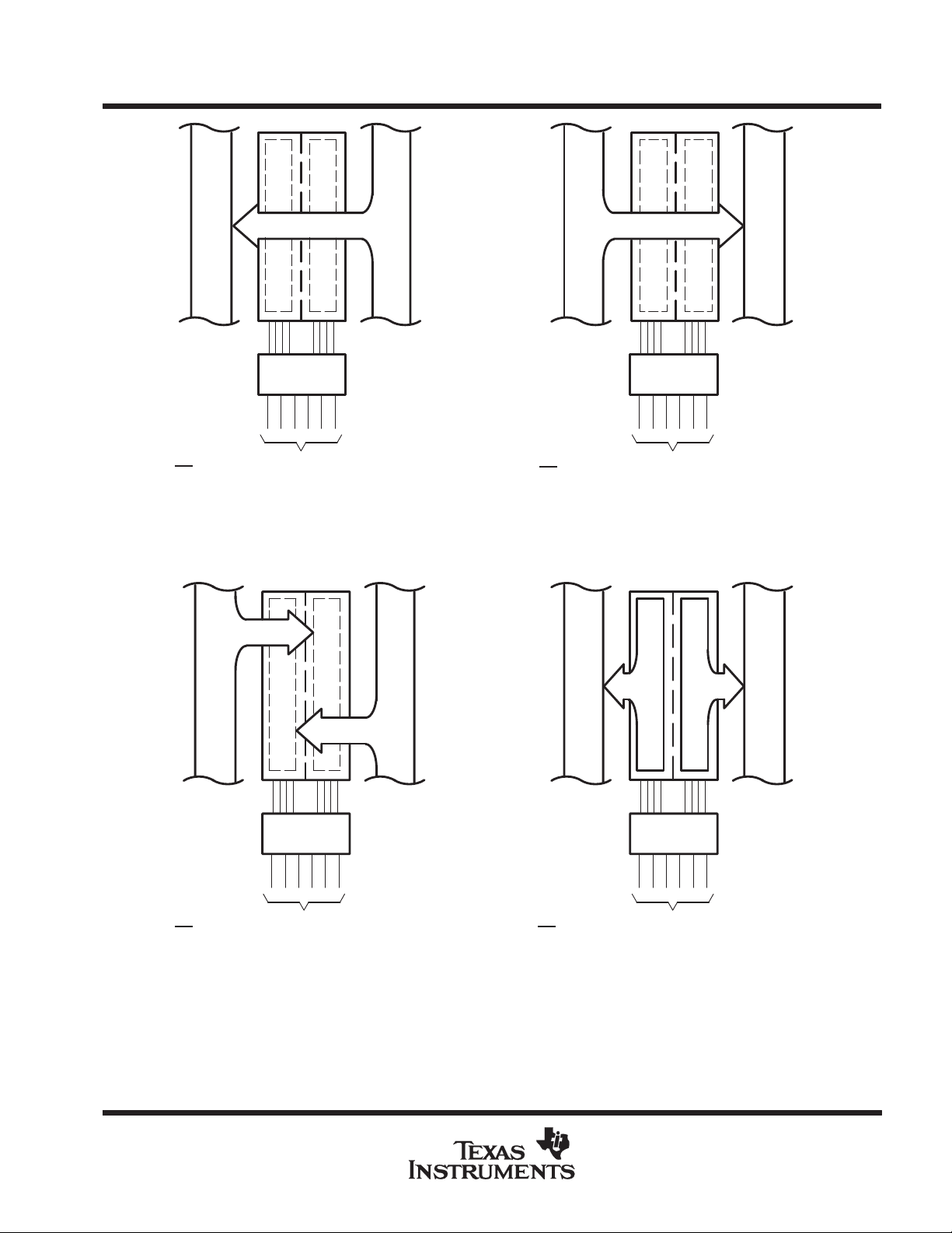
Transceiver function is controlled by output-enable (OE
transceiver is active and operates in the A-to-B direction when DIR is high or in the B-to-A direction when DIR
is low. When OE is high, both the A and B outputs are in the high-impedance state, effectively isolating both
buses.
Data flow is controlled by clock (CLKAB and CLKBA) and select (SAB and SBA) inputs. Data on the A bus is
clocked into the associated registers on the low-to-high transition of CLKAB. When SAB is low, real-time A data
is selected for presentation to the B bus (transparent mode). When SAB is high, stored A data is selected for
presentation to the B bus (registered mode). The function of the CLKBA and SBA inputs mirrors that of CLKAB
and SAB, respectively. Figure 1 illustrates the four fundamental bus-management functions that can be
performed with the ′ABT18646.
) and direction (DIR) inputs. When OE is low, the
2
POST OFFICE BOX 655303 • DALLAS, TEXAS 75265
SN54ABT18646, SN74ABT18646
OPERATION OR FUNCTION
SCAN TEST DEVICES WITH
18-BIT TRANSCEIVERS AND REGISTERS
SCBS131–AUGUST 1992–REVISED OCTOBER 1992
description (continued)
In the test mode, the normal operation of the SCOPE bus transceivers and registers is inhibited, and the test
circuitry is enabled to observe and control the I/O boundary of the device. When enabled, the test circuitry can
perform boundary scan test operations according to the protocol described in IEEE Standard 1149.1-1990.
Four dedicated test pins are used to observe and control the operation of the test circuitry: test data input (TDI),
test data output (TDO), test mode select (TMS), and test clock (TCK). Additionally , the test circuitry can perform
other testing functions such as parallel signature analysis on data inputs and pseudo-random pattern generation
from data outputs. All testing and scan operations are synchronized to the TAP interface.
Additional flexibility is provided in the test mode through the use of two boundary scan cells (BSCs) for each
I/O pin. This allows independent test data to be captured and forced at either bus (A or B). A PSA/COUNT
instruction is also included to ease the testing of memories and other circuits where a binary count addressing
scheme is useful.
The SN54ABT18646 is characterized over the full military temperature range of –55°C to 125°C. The
SN74ABT18646 is characterized for operation from –40°C to 85°C.
FUNCTION TABLE
(normal mode, each 9-bit section)
INPUTS
OE DIR CLKAB CLKBA SAB SBA A1 THRU A9 B1 THRU B9
X X ↑ X X X Input Unspecified
X XX ↑ X X Unspecified
H X ↑ ↑ X X Input Input Store A and B data
H X L L X X Input disabled Input disabled Isolation, hold storage
L L X X X L Output Input Real-time B data to A bus
L L X L X H Output Input disabled Stored B data to A bus
L H X X L X Input Output Real-time A data to B bus
L H L X H X Input disabled Output Stored A data to B bus
†
The data output functions can be enabled or disabled by various signals at the OE and DIR inputs. Data input functions are always enabled; i.e.,
data at the bus pins will be stored on every low-to-high transition of the clock inputs.
DATA I/O
†
†
Input Store B, A unspecified
Store A, B unspecified
†
†
POST OFFICE BOX 655303 • DALLAS, TEXAS 75265
PRODUCT PREVIEW
3
SN54ABT18646, SN74ABT18646
SCAN TEST DEVICES WITH
18-BIT TRANSCEIVERS AND REGISTERS
SCBS131–AUGUST 1992–REVISED OCTOBER 1992
BUS A
PRODUCT PREVIEW
DIRLCLKABXCLKBAXSABXSBA
OE
L
REAL-TIME TRANSFER
BUS B TO BUS A
BUS B
L
OE
L
BUS A
DIRHCLKABXCLKBAXSABLSBA
REAL-TIME TRANSFER
BUS A TO BUS B
BUS B
X
BUS A
DIRXCLKAB CLKBAXSABXSBA
X
X
H
X
X
↑
XX
STORAGE FROM
A, B, OR A AND B
↑
↑↑
BUS B
X
X
X
X
OEOE
BUS A
DIRLCLKABXCLKBALSABXSBA
L
LH L XHX
TRANSFER STORED DA TA
Figure 1. Bus-Management Functions
BUS B
H
TO A AND/OR B
4
POST OFFICE BOX 655303 • DALLAS, TEXAS 75265
 Loading...