

SN54ABT16623, SN74ABT16623
16-BIT BUS TRANSCEIVERS
WITH 3-STATE OUTPUTS
SCBS211B – FEBRUAR Y 1991 – REVISED JANUAR Y 1997
D
Members of the Texas Instruments
Widebus
D
State-of-the-Art
Family
EPIC-ΙΙB
BiCMOS Design
Significantly Reduces Power Dissipation
D
Latch-Up Performance Exceeds 500 mA Per
JEDEC Standard JESD-17
D
T ypical V
(Output Ground Bounce) < 1 V
OLP
at VCC = 5 V, TA = 25°C
D
Distributed VCC and GND Pin Configuration
Minimizes High-Speed Switching Noise
D
Flow-Through Architecture Optimizes PCB
Layout
D
High-Drive Outputs (–32-mA IOH, 64-mA IOL)
D
Package Options Include Plastic 300-mil
Shrink Small-Outline (DL) and Thin Shrink
Small-Outline (DGG) Packages and 380-mil
Fine-Pitch Ceramic Flat (WD) Package
Using 25-mil Center-to-Center Spacings
description
The ’ABT16623 are 16-bit transceivers designed
for asynchronous communication between data
buses. The control-function implementation
allows for maximum flexibility in timing. The
’ABT16623 provide true data at the outputs.
These devices can be used as two 8-bit
transceivers or one 16-bit transceiver. They allow
data transmission from the A bus to the B bus or
from the B bus to the A bus, depending on the logic
levels at the output-enable (OEAB and OEBA
inputs. The output-enable inputs can be used to
disable the device so that the buses are effectively
isolated. The dual-enable configuration gives the
transceivers the capability of storing data by
simultaneously enabling OEAB and OEBA
output reinforces its input in this configuration.
When both OEAB and OEBA are enabled and all
other data sources to the two sets of bus lines are
at high impedance, both sets of bus lines (32 total)
remain at their last states.
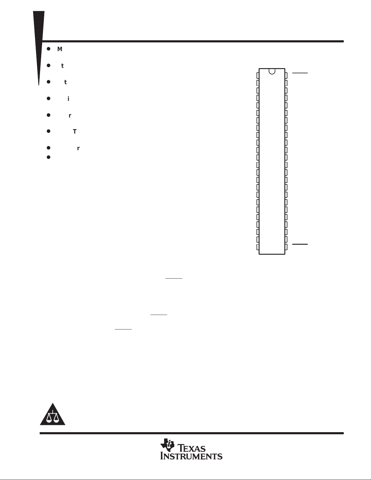
. Each
SN54ABT16623 . . . WD PACKAGE
SN74ABT16623 . . . DGG OR DL PACKAGE
1OEAB
2OEAB
1B1
1B2
GND
1B3
1B4
V
CC
1B5
1B6
GND
1B7
1B8
2B1
2B2
GND
2B3
2B4
V
CC
2B5
2B6
GND
2B7
2B8
(TOP VIEW)
1
48
2
47
3
46
4
45
5
44
6
43
7
42
8
41
9
40
10
39
11
38
12
37
13
36
14
35
15
34
16
33
17
32
18
31
19
30
20
29
21
28
22
27
23
26
24
25
1OEBA
1A1
1A2
GND
1A3
1A4
V
CC
1A5
1A6
GND
1A7
1A8
2A1
2A2
GND
2A3
2A4
V
CC
2A5
2A6
GND
2A7
2A8
2OEBA
)
Please be aware that an important notice concerning availability, standard warranty, and use in critical applications of
Texas Instruments semiconductor products and disclaimers thereto appears at the end of this data sheet.
Widebus and EPIC-ΙΙB are trademarks of Texas Instruments Incorporated.
UNLESS OTHERWISE NOTED this document contains PRODUCTION
DATA information current as of publication date. Products conform to
specifications per the terms of Texas Instruments standard warranty.
Production processing does not necessarily include testing of all
parameters.
POST OFFICE BOX 655303 • DALLAS, TEXAS 75265
Copyright 1997, Texas Instruments Incorporated
1
SN54ABT16623, SN74ABT16623
OPERATION
16-BIT BUS TRANSCEIVERS
WITH 3-STATE OUTPUTS
SCBS211B – FEBRUAR Y 1991 – REVISED JANUAR Y 1997
description (continued)
To ensure the high-impedance state during power up or power down, OEBA should be tied to VCC through a
pullup resistor; the minimum value of the resistor is determined by the current-sinking capability of the driver.
OEAB should be tied to GND through a pulldown resistor; the minimum value of the resistor is determined by
the current-sourcing capability of the driver.
The SN54ABT16623 is characterized for operation over the full military temperature range of –55°C to 125°C.
The SN74ABT16623 is characterized for operation from –40°C to 85°C.
FUNCTION TABLE
(each 8-bit section)
INPUTS
OEBA
OEAB
L L B data to A bus
L H
H L Isolation
H H A data to B bus
B data to A bus,
A data to B bus
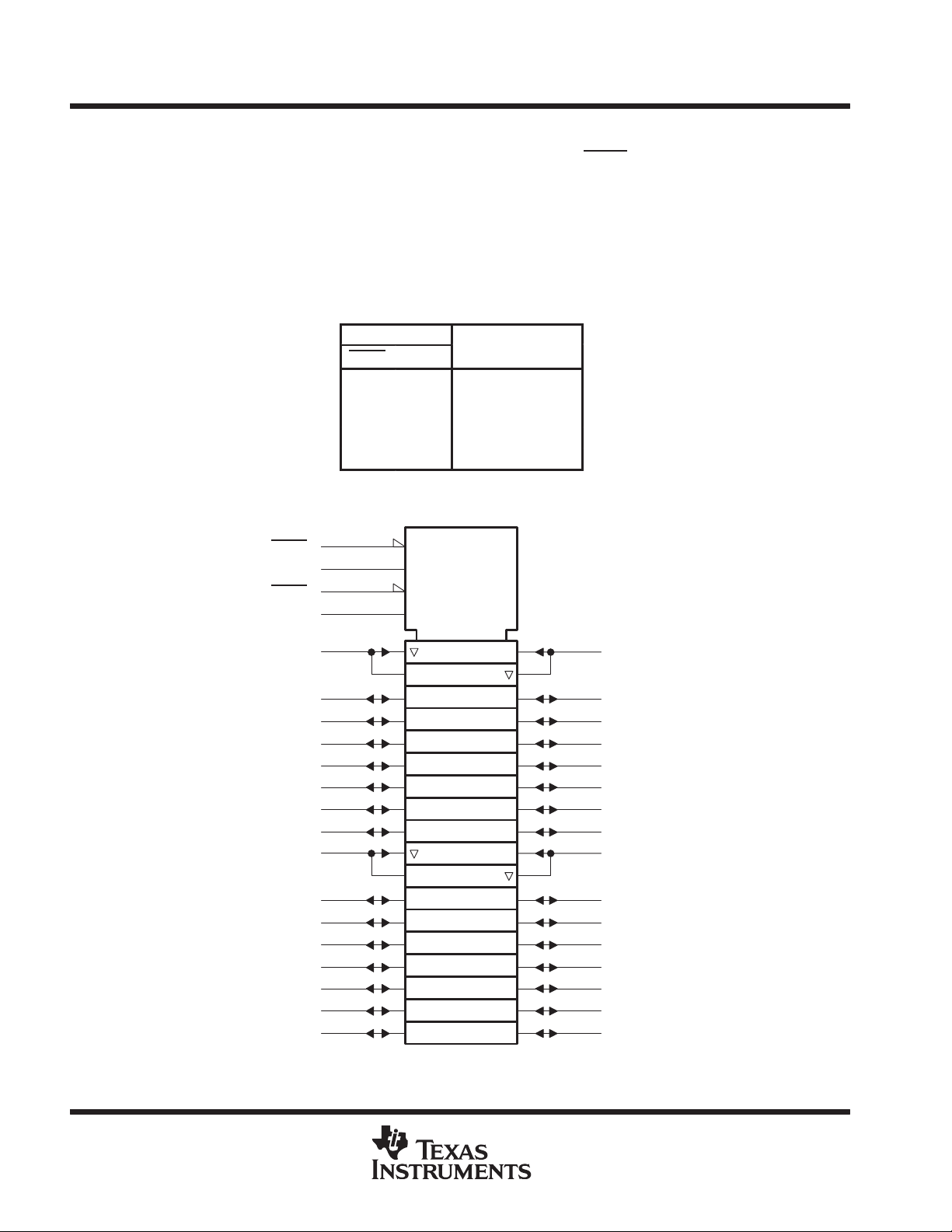
logic symbol
†
1OEBA
1OEAB
2OEBA
2OEAB
1A1
1A2
1A3
1A4
1A5
1A6
1A7
1A8
2A1
2A2
2A3
2A4
2A5
2A6
2A7
2A8
48
1
25
24
47
46
44
43
41
40
38
37
36
35
33
32
30
29
27
26
EN1
EN2
EN3
EN4
1
3
1
12
1
14
11
12
13
14
16
17
19
20
22
23
2
1B1
3
1B2
5
1B3
6
1B4
8
1B5
9
1B6
1B7
1B8
2B1
2B2
2B3
2B4
2B5
2B6
2B7
2B8
†
This symbol is in accordance with ANSI/IEEE Std 91-1984 and IEC Publication 617-12.
2
POST OFFICE BOX 655303 • DALLAS, TEXAS 75265
UNIT
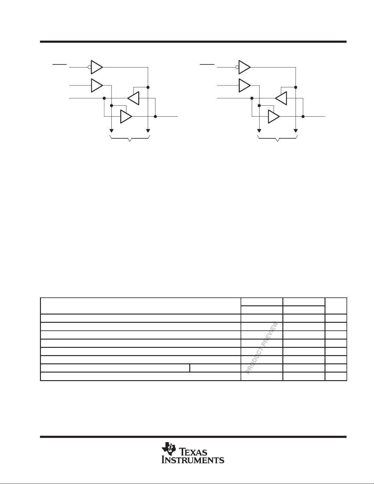
logic diagram (positive logic)
SN54ABT16623, SN74ABT16623
16-BIT BUS TRANSCEIVERS
WITH 3-STATE OUTPUTS
SCBS211B – FEBRUAR Y 1991 – REVISED JANUAR Y 1997
1OEBA
1OEBA
1OEBA
48
1
47
To Seven Other Channels
2OEBA
2OEBA
2OEBA
2
1B1
25
24
36
To Seven Other Channels
13
2B1
absolute maximum ratings over operating free-air temperature range (unless otherwise noted)
Supply voltage range, VCC –0.5 V to 7 V. . . . . . . . . . . . . . . . . . . . . . . . . . . . . . . . . . . . . . . . . . . . . . . . . . . . . . . . . .
Input voltage range, VI (except I/O ports) (see Note 1) –0.5 V to 7 V. . . . . . . . . . . . . . . . . . . . . . . . . . . . . . . . . .
Voltage range applied to any output in the high or power-off state, VO –0.5 V to 5.5 V. . . . . . . . . . . . . . . . . . .
Current into any output in the low state, IO: SN54ABT16623 96 mA. . . . . . . . . . . . . . . . . . . . . . . . . . . . . . . . . .
SN74ABT16623 128 mA. . . . . . . . . . . . . . . . . . . . . . . . . . . . . . . . .
Input clamp current, I
Output clamp current, IOK (VO < 0) –50 mA. . . . . . . . . . . . . . . . . . . . . . . . . . . . . . . . . . . . . . . . . . . . . . . . . . . . . . . .
Package thermal impedance, θ
Storage temperature range, T
†
Stresses beyond those listed under “absolute maximum ratings” may cause permanent damage to the device. These are stress ratings only, and
functional operation of the device at these or any other conditions beyond those indicated under “recommended operating conditions” is not
implied. Exposure to absolute-maximum-rated conditions for extended periods may affect device reliability.
NOTES: 1. The input and output negative-voltage ratings may be exceeded if the input and output clamp-current ratings are observed.
2. The package thermal impedance is calculated in accordance with EIA/JEDEC Std JESD51.
(VI < 0) –18 mA. . . . . . . . . . . . . . . . . . . . . . . . . . . . . . . . . . . . . . . . . . . . . . . . . . . . . . . . . . .
IK
(see Note 2): DGG package 89°C/W. . . . . . . . . . . . . . . . . . . . . . . . . . . . . . .
JA
DL package 94°C/W. . . . . . . . . . . . . . . . . . . . . . . . . . . . . . . . .
–65°C to 150°C. . . . . . . . . . . . . . . . . . . . . . . . . . . . . . . . . . . . . . . . . . . . . . . . . . .
stg
†
recommended operating conditions (see Note 3)
SN54ABT16623 SN74ABT16623
MIN MAX MIN MAX
V
V
V
V
I
OH
I
OL
∆t/∆v Input transition rise or fall rate Outputs enabled 5 5 ns/V
T
NOTE 3: Unused pins (input or I/O) must be held high or low to prevent them from floating.
PRODUCT PREVIEW information concerns products in the formative or
design phase of development. Characteristic data and other
specifications are design goals. Texas Instruments reserves the right to
change or discontinue these products without notice.
Supply voltage 4.5 5.5 4.5 5.5 V
CC
High-level input voltage 2 2 V
IH
Low-level input voltage 0.8 0.8 V
IL
Input voltage 0 V
I
High-level output current –24 –32 mA
Low-level output current 48 64 mA
Operating free-air temperature –55 125 –40 85 °C
A
POST OFFICE BOX 655303 • DALLAS, TEXAS 75265
CC
0 V
CC
V
3
 Loading...