

Texas Instruments SN74ABT16543DGGR, SN74ABT16543DL, SN74ABT16543DLR, SNJ54ABT16543WD Datasheet
SN54ABT16543, SN74ABT16543
16-BIT REGISTERED TRANSCEIVERS
WITH 3-STATE OUTPUTS
SCBS087C – FEBRUARY 1991 – REVISED JANUARY 1997
D
Members of the Texas Instruments
Widebus
D
State-of-the-Art
Family
EPIC-ΙΙB
BiCMOS Design
Significantly Reduces Power Dissipation
D
Latch-Up Performance Exceeds 500 mA Per
JEDEC Standard JESD-17
D
T ypical V
(Output Ground Bounce) < 1 V
OLP
at VCC = 5 V, TA = 25°C
D
Distributed VCC and GND Pin Configuration
Minimizes High-Speed Switching Noise
D
Flow-Through Architecture Optimizes PCB
Layout
D
High-Drive Outputs (–32-mA IOH, 64-mA IOL)
D
Package Options Include Plastic 300-mil
Shrink Small-Outline (DL) and Thin Shrink
Small-Outline (DGG) Packages and 380-mil
Fine-Pitch Ceramic Flat (WD) Package
Using 25-mil Center-to-Center Spacings
description
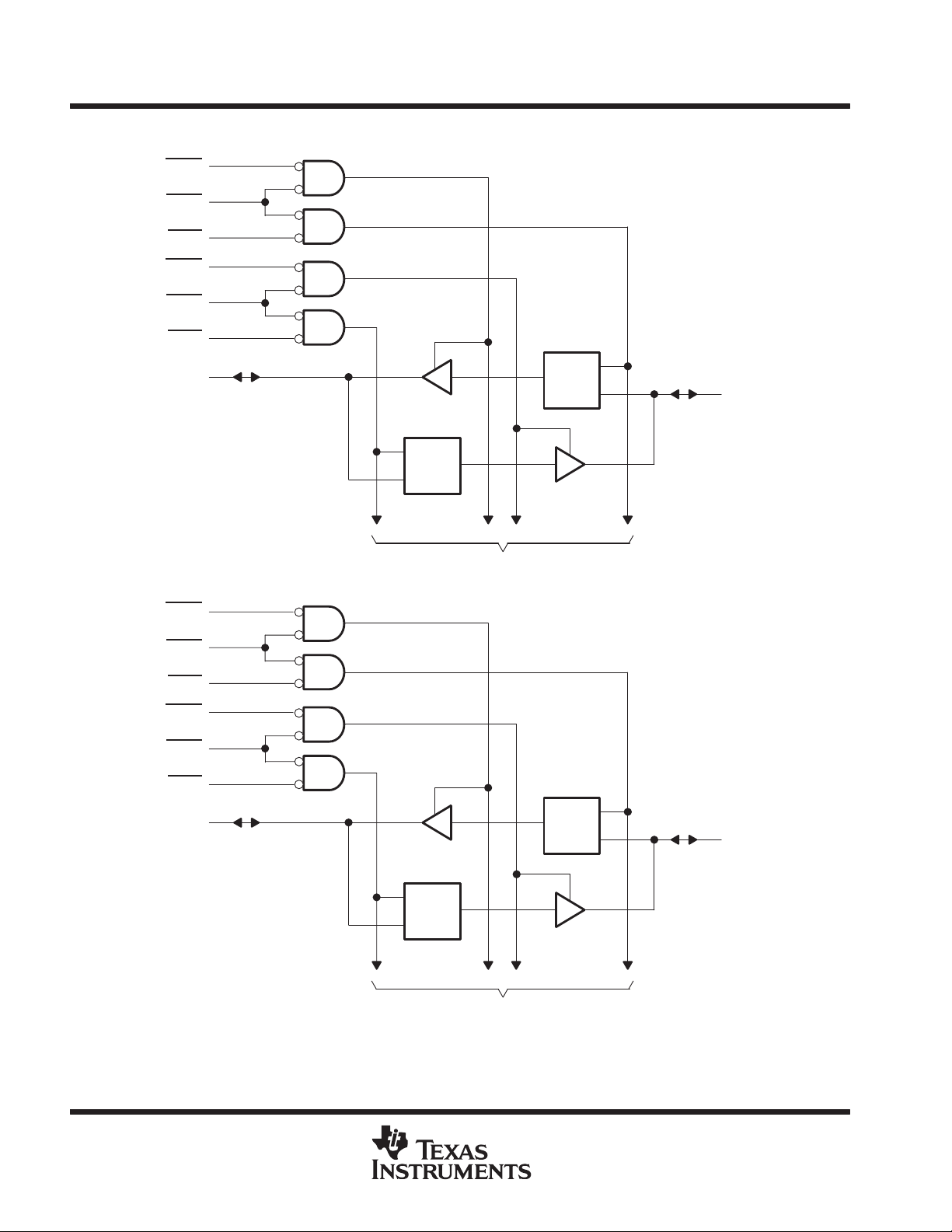
The ’ABT16543 16-bit registered transceivers
contain two sets of D-type latches for temporary
storage of data flowing in either direction. The
’ABT16543 can be used as two 8-bit transceivers
or one 16-bit transceiver. Separate latch-enable
(LEAB
or LEBA) and output-enable (OEAB or
OEBA
) inputs are provided for each register to
permit independent control in either direction of
data flow.
The A-to-B enable (CEAB) input must be low to
enter data from A or to output data from B. If CEAB
is low and LEAB is low, the A-to-B latches are
transparent; a subsequent low-to-high transition
of LEAB puts the A latches in the storage mode.
With CEAB
B outputs are active and reflect the data present
at the output of the A latches. Data flow from B to
A is similar but requires using the CEBA, LEBA,
and OEBA inputs.
and OEAB both low, the 3-state
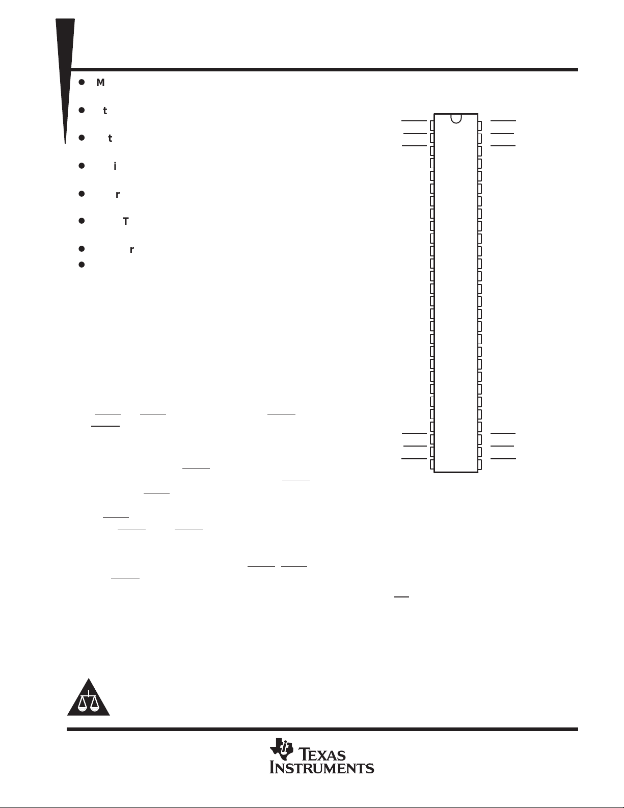
SN54ABT16543 . . . WD PACKAGE
SN74ABT16543 . . . DGG OR DL PACKAGE
1OEAB
1LEAB
1CEAB
2CEAB
2LEAB
2OEAB
GND
1A1
1A2
V
CC
1A3
1A4
1A5
GND
1A6
1A7
1A8
2A1
2A2
2A3
GND
2A4
2A5
2A6
V
CC
2A7
2A8
GND
(TOP VIEW)
1
56
2
55
3
54
4
53
5
52
6
51
7
50
8
49
9
48
10
47
11
46
12
45
13
44
14
43
15
42
16
41
17
40
18
39
19
38
20
37
21
36
22
35
23
34
24
33
25
32
26
31
27
30
28
29
1OEBA
1LEBA
1CEBA
GND
1B1
1B2
V
CC
1B3
1B4
1B5
GND
1B6
1B7
1B8
2B1
2B2
2B3
GND
2B4
2B5
2B6
V
CC
2B7
2B8
GND
2CEBA
2LEBA
2OEBA
T o ensure the high-impedance state during power up or power down, OE should be tied to VCC through a pullup
resistor; the minimum value of the resistor is determined by the current-sinking capability of the driver.
The SN54ABT16543 is characterized for operation over the full military temperature range of –55°C to 125°C.
The SN74ABT16543 is characterized for operation from –40°C to 85°C.
Please be aware that an important notice concerning availability, standard warranty, and use in critical applications of
Texas Instruments semiconductor products and disclaimers thereto appears at the end of this data sheet.
Widebus and EPIC-ΙΙB are trademarks of Texas Instruments Incorporated.
PRODUCTION DATA information is current as of publication date.
Products conform to specifications per the terms of Texas Instruments
standard warranty. Production processing does not necessarily include
testing of all parameters.
POST OFFICE BOX 655303 • DALLAS, TEXAS 75265
Copyright 1997, Texas Instruments Incorporated
1
SN54ABT16543, SN74ABT16543
16-BIT REGISTERED TRANSCEIVERS
WITH 3-STATE OUTPUTS
SCBS087C – FEBRUARY 1991 – REVISED JANUARY 1997
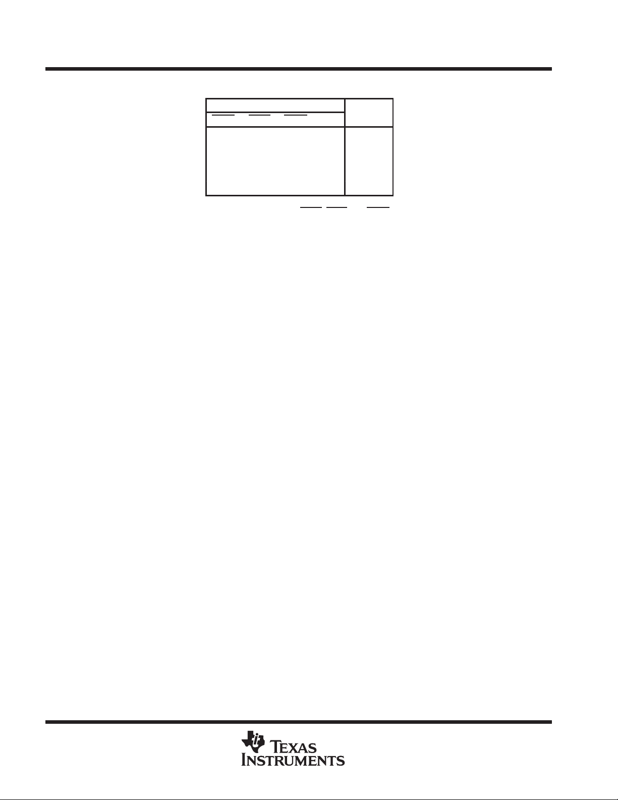
FUNCTION TABLE
(each 8-bit section)
INPUTS
CEAB LEAB OEAB A
H X X X Z
X XHX Z
L HLXB
L LLL L
L L L H H
†
A-to-B data flow is shown; B-to-A flow control is the
same except that it uses CEBA
‡
Output level before the indicated steady-state input
conditions were established
†
OUTPUT
B
‡
0
, LEBA, and OEBA.
2
POST OFFICE BOX 655303 • DALLAS, TEXAS 75265
SN54ABT16543, SN74ABT16543
16-BIT REGISTERED TRANSCEIVERS
WITH 3-STATE OUTPUTS
SCBS087C – FEBRUARY 1991 – REVISED JANUARY 1997
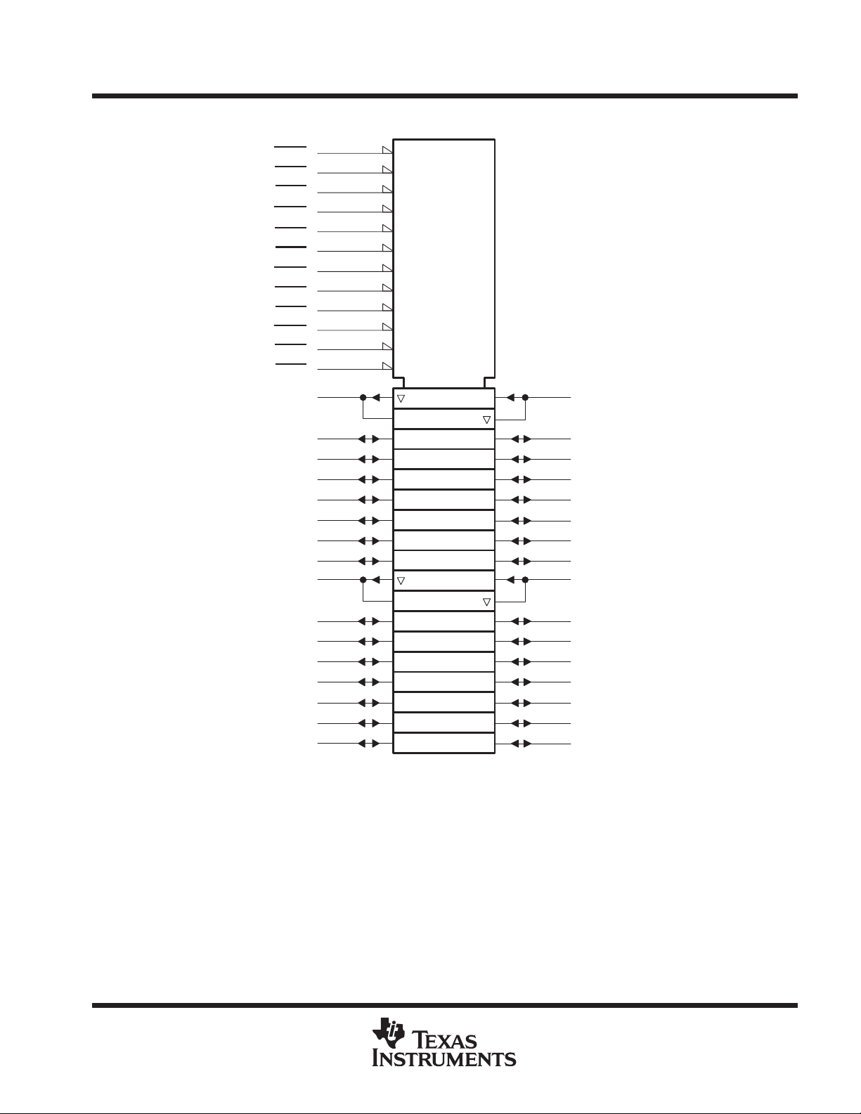
logic symbol
†
1OEBA
1CEBA
1LEBA
1OEAB
1CEAB
1LEAB
2OEBA
2CEBA
2LEBA
2OEAB
2CEAB
2LEAB
1A1
1A2
1A3
1A4
1A5
1A6
1A7
1A8
2A1
2A2
2A3
2A4
2A5
2A6
2A7
2A8
56
54
55
1
3
2
29
31
30
28
26
27
5
6
8
9
10
12
13
14
15
16
17
19
20
21
23
24
1EN3
G1
1C5
2EN4
G2
2C6
7EN9
G7
7C11
8EN10
G8
8C12
3
6D
9
12D
5D
4
11D
10
52
51
49
48
47
45
44
43
42
41
40
38
37
36
34
33
1B1
1B2
1B3
1B4
1B5
1B6
1B7
1B8
2B1
2B2
2B3
2B4
2B5
2B6
2B7
2B8
†
This symbol is in accordance with ANSI/IEEE Std 91-1984 and IEC Publication 617-12.
POST OFFICE BOX 655303 • DALLAS, TEXAS 75265
3
SN54ABT16543, SN74ABT16543
16-BIT REGISTERED TRANSCEIVERS
WITH 3-STATE OUTPUTS
SCBS087C – FEBRUARY 1991 – REVISED JANUARY 1997
logic diagram (positive logic)
1OEBA
1CEBA
1LEBA
1OEAB
1CEAB
1LEAB
1A1
2OEBA
56
54
55
1
3
2
5
29
C1
1D
To Seven Other Channels
C1
1D
52
1B1
2CEBA
2LEBA
2OEAB
2CEAB
2LEAB
2A1
31
30
28
26
27
15
C1
1D
To Seven Other Channels
C1
1D
42
2B1
4
POST OFFICE BOX 655303 • DALLAS, TEXAS 75265
UNIT
SN54ABT16543, SN74ABT16543
16-BIT REGISTERED TRANSCEIVERS
WITH 3-STATE OUTPUTS
SCBS087C – FEBRUARY 1991 – REVISED JANUARY 1997
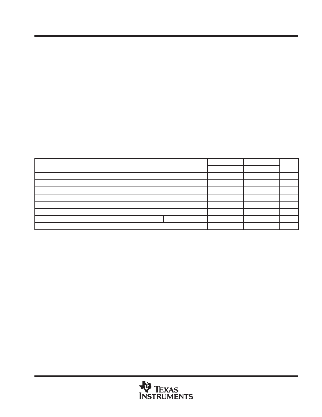
absolute maximum ratings over operating free-air temperature range (unless otherwise noted)
Supply voltage range, V
Input voltage range, VI (except I/O ports) (see Note 1) –0.5 V to 7 V. . . . . . . . . . . . . . . . . . . . . . . . . . . . . . . . . .
Voltage range applied to any output in the high or power-off state, VO –0.5 V to 5.5 V. . . . . . . . . . . . . . . . . . .
Current into any output in the low state, IO: SN54ABT16543 96 mA. . . . . . . . . . . . . . . . . . . . . . . . . . . . . . . . . .
Input clamp current, I
Output clamp current, IOK (VO < 0) –50 mA. . . . . . . . . . . . . . . . . . . . . . . . . . . . . . . . . . . . . . . . . . . . . . . . . . . . . . . .
Package thermal impedance, θ
Storage temperature range, T
†
Stresses beyond those listed under “absolute maximum ratings” may cause permanent damage to the device. These are stress ratings only, and
functional operation of the device at these or any other conditions beyond those indicated under “recommended operating conditions” is not
implied. Exposure to absolute-maximum-rated conditions for extended periods may affect device reliability.
NOTES: 1. The input and output negative-voltage ratings may be exceeded if the input and output clamp-current ratings are observed.
2. The package thermal impedance is calculated in accordance with EIA/JEDEC Std JESD51.
–0.5 V to 7 V. . . . . . . . . . . . . . . . . . . . . . . . . . . . . . . . . . . . . . . . . . . . . . . . . . . . . . . . . .
CC
SN74ABT16543 128 mA. . . . . . . . . . . . . . . . . . . . . . . . . . . . . . . . .
(VI < 0) –18 mA. . . . . . . . . . . . . . . . . . . . . . . . . . . . . . . . . . . . . . . . . . . . . . . . . . . . . . . . . . .
IK
(see Note 2): DGG package 81°C/W. . . . . . . . . . . . . . . . . . . . . . . . . . . . . . .
JA
DL package 74°C/W. . . . . . . . . . . . . . . . . . . . . . . . . . . . . . . . .
–65°C to 150°C. . . . . . . . . . . . . . . . . . . . . . . . . . . . . . . . . . . . . . . . . . . . . . . . . . .
stg
recommended operating conditions (see Note 3)
SN54ABT16543 SN74ABT16543
MIN MAX MIN MAX
V
V
V
V
I
OH
I
OL
∆t/∆v Input transition rise or fall rate Outputs enabled 10 10 ns/V
T
NOTE 3: Unused pins (input or I/O) must be held high or low to prevent them from floating.
Supply voltage 4.5 5.5 4.5 5.5 V
CC
High-level input voltage 2 2 V
IH
Low-level input voltage 0.8 0.8 V
IL
Input voltage 0 V
I
High-level output current –24 –32 mA
Low-level output current 48 64 mA
Operating free-air temperature –55 125 –40 85 °C
A
CC
0 V
CC
V
†
POST OFFICE BOX 655303 • DALLAS, TEXAS 75265
5
SN54ABT16543, SN74ABT16543
PARAMETER
TEST CONDITIONS
UNIT
V
V
V
4.5 V
VOLV
V
V
µ
I
CC,ICC
µ
V
CC
t
S
LEAB↑
LEBA↑
ns
t
Hold ti
LEAB↑
LEBA↑
ns
16-BIT REGISTERED TRANSCEIVERS
WITH 3-STATE OUTPUTS
SCBS087C – FEBRUARY 1991 – REVISED JANUARY 1997
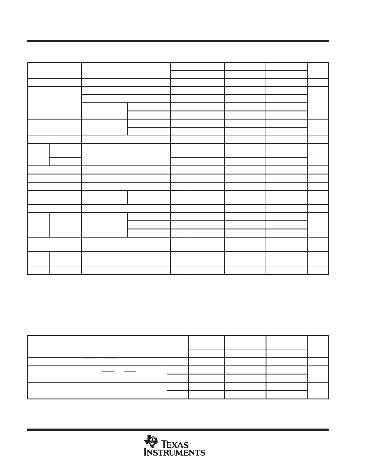
electrical characteristics over recommended operating free-air temperature range (unless
otherwise noted)
TA = 25°C SN54ABT16543 SN74ABT16543
MIN TYP†MAX MIN MAX MIN MAX
V
IK
OH
V
hys
Control
I
I
OZH
I
OZL
I
off
I
CEX
I
O
I
CC
∆I
C
C
* On products compliant to MIL-PRF-38535, this parameter does not apply.
** These limits apply only to the SN74ABT16543.
†
All typical values are at VCC = 5 V.
‡
The parameters I
§
Not more than one output should be tested at a time, and the duration of the test should not exceed one second.
¶
This is the increase in supply current for each input that is at the specified TTL voltage level rather than VCC or GND.
inputs
A or B ports
‡
‡
§
A or B ports
¶
CC
Control
i
inputs
A or B ports VO = 2.5 V or 0.5 V 8.5 pF
io
VCC = 4.5 V, II = –18 mA –1.2 –1.2 –1.2 V
VCC = 4.5 V, IOH = –3 mA 2.5 2.5 2.5
VCC = 5 V, IOH = –3 mA 3 3 3
=
CC
= 4.5
CC
V
= 5.5 V, V
VCC = 5.5 V, VO = 2.7 V 50** 10 50 µA
VCC = 5.5 V, VO = 0.5 V –50** –10 –50 µA
VCC = 0, VI or VO ≤ 4.5 V ±100 ±100 µA
VCC = 5.5 V,
VO = 5.5 V
VCC = 5.5 V, VO = 2.5 V –50 –100 –200 –50 –200 –50 –200 mA
=
= 5.5 V,
IO = 0,
VI = VCC or GND
VCC = 5.5 V, One input at 3.4 V,
Other inputs at VCC or GND
VI = 2.5 V or 0.5 V 3 pF
OZH
and I
include the input leakage current.
OZL
IOH = –24 mA 2 2
IOH = –32 mA 2* 2
IOL = 48 mA 0.55 0.55
IOL = 64 mA 0.55* 0.55
100 mV
= V
or GND
Outputs high 50 50 50 µA
Outputs high 2 2 2
Outputs low 35 35 35
Outputs disabled 2 2 2
±1 ±1 ±1
±100 ±100 ±100
0.5 0.5 0.5 mA
A
mA
timing requirements over recommended ranges of supply voltage and operating free-air
temperature (unless otherwise noted) (see Figure 1)
t
w
su
h
6
Pulse duration, LEAB or LEBA low 4 4 4 ns
etup time, data before
me, data after
or
or
POST OFFICE BOX 655303 • DALLAS, TEXAS 75265
High 1.5 1.5 1.5
Low 3.5 3.5 3.5
High 1.5 1.5 1.5
Low 2 2 2
VCC = 5 V,
TA = 25°C
MIN MAX MIN MAX MIN MAX
SN54ABT16543 SN74ABT16543
UNIT
A or B
B or A
ns
LE
A or B
ns
OE
A or B
ns
OE
A or B
ns
CE
A or B
ns
CE
A or B
ns
A or B
B or A
ns
LE
A or B
ns
OE
A or B
ns
OE
A or B
ns
CE
A or B
ns
CE
A or B
ns
SN54ABT16543, SN74ABT16543
16-BIT REGISTERED TRANSCEIVERS
WITH 3-STATE OUTPUTS
SCBS087C – FEBRUARY 1991 – REVISED JANUARY 1997
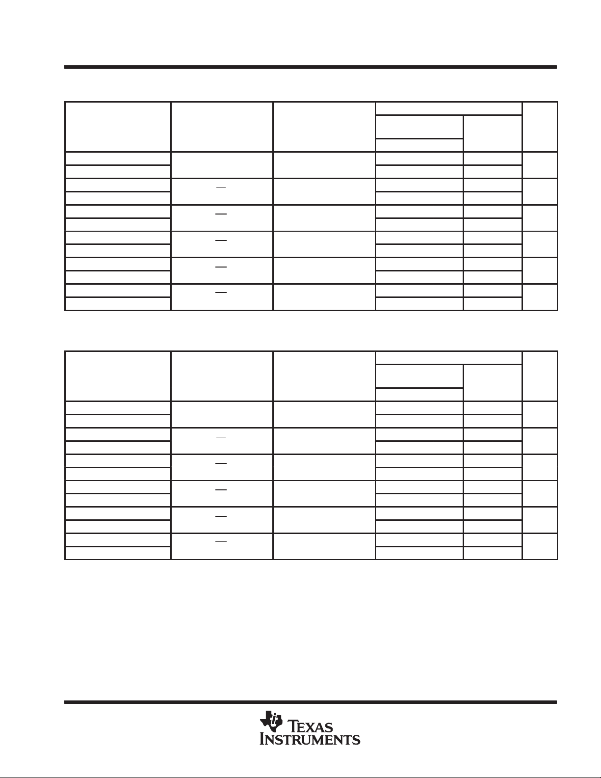
switching characteristics over recommended ranges of supply voltage and operating free-air
temperature, C
PARAMETER
t
PLH
t
PHL
t
PLH
t
PHL
t
PZH
t
PZL
t
PHZ
t
PLZ
t
PZH
t
PZL
t
PHZ
t
PLZ
= 50 pF (unless otherwise noted) (see Figure 1)
L
FROM
(INPUT)
TO
(OUTPUT)
SN54ABT16543
VCC = 5 V,
TA = 25°C
MIN TYP MAX
0.8 2.5 3.3 0.8 3.9
0.9 2.7 4.4 0.9 5.2
1 3.1 4.3 1 5.3
1.2 3.3 4.8 1.2 5.7
0.8 3.4 4.3 0.8 5.3
1.1 3.8 7 1.1 7.9
1.9 4 6.3 1.9 7.2
1.6 3.3 4.6 1.6 5
0.9 3.8 4.9 0.9 6.3
1.2 4.2 6.8 1.2 7.9
2 4.5 6.4 2 7.3
1.7 3.9 5.1 1.7 5.6
MIN MAX
UNIT
switching characteristics over recommended ranges of supply voltage and operating free-air
temperature, C
PARAMETER
t
PLH
t
PHL
t
PLH
t
PHL
t
PZH
t
PZL
t
PHZ
t
PLZ
t
PZH
t
PZL
t
PHZ
t
PLZ
= 50 pF (unless otherwise noted) (see Figure 1)
L
FROM
(INPUT)
TO
(OUTPUT)
SN74ABT16543
VCC = 5 V,
TA = 25°C
MIN TYP MAX
1 2.5 3.3 1 3.8
1 2.7 4.4 1 5.1
1 3.1 4.3 1 5.2
1.2 3.3 4.8 1.2 5.6
1 3.4 4.3 1 5.2
1.1 3.8 5.9 1.1 7
1.9 4 5 1.9 5.7
1.6 3.3 4.2 1.6 4.6
1 3.8 4.9 1 6.2
1.2 4.2 6.5 1.2 7.8
2 4.5 5.6 2 6.6
1.7 3.9 5.1 1.7 5.4
MIN MAX
UNIT
POST OFFICE BOX 655303 • DALLAS, TEXAS 75265
7

SN54ABT16543, SN74ABT16543
16-BIT REGISTERED TRANSCEIVERS
WITH 3-STATE OUTPUTS
SCBS087C – FEBRUARY 1991 – REVISED JANUARY 1997
PARAMETER MEASUREMENT INFORMATION
500 Ω
t
w
1.5 V
500 Ω
1.5 V
From Output
Under Test
CL = 50 pF
(see Note A)
LOAD CIRCUIT
Input
Input
Output
Output
INVERTING AND NONINVERTING OUTPUTS
NOTES: A. CL includes probe and jig capacitance.
B. Waveform 1 is for an output with internal conditions such that the output is low except when disabled by the output control.
Waveform 2 is for an output with internal conditions such that the output is high except when disabled by the output control.
C. All input pulses are supplied by generators having the following characteristics: PRR ≤ 10 MHz, ZO = 50 Ω, tr ≤ 2.5 ns, tf≤ 2.5 ns.
D. The outputs are measured one at a time with one transition per measurement.
1.5 V
VOLTAGE WAVEFORMS
PULSE DURATION
1.5 V 1.5 V
t
PLH
t
PHL
VOLTAGE WAVEFORMS
PROPAGATION DELAY TIMES
S1
t
PHL
1.5 V
t
PLH
1.5 V1.5 V
3 V
0 V
V
V
V
V
7 V
OH
OL
OH
OL
Open
GND
3 V
0 V
Timing Input
Data Input
Output
Output
Control
Control
Output
Waveform 1
S1 at 7 V
(see Note B)
Output
Waveform 2
S1 at Open
(see Note B)
TEST S1
t
PLH/tPHL
t
PLZ/tPZL
t
PHZ/tPZH
t
su
1.5 V 1.5 V
VOLTAGE WAVEFORMS
SETUP AND HOLD TIMES
t
PZL
t
PLZ
1.5 V
t
t
PZH
VOLTAGE WAVEFORMS
ENABLE AND DISABLE TIMES
LOW- AND HIGH-LEVEL ENABLING
PHZ
1.5 V
Open
Open
1.5 V
t
7 V
h
1.5 V1.5 V
VOL + 0.3 V
VOH – 0.3 V
3 V
0 V
3 V
0 V
3 V
0 V
3.5 V
V
OL
V
OH
≈ 0 V
Figure 1. Load Circuit and Voltage Waveforms
8
POST OFFICE BOX 655303 • DALLAS, TEXAS 75265

IMPORTANT NOTICE
T exas Instruments and its subsidiaries (TI) reserve the right to make changes to their products or to discontinue
any product or service without notice, and advise customers to obtain the latest version of relevant information
to verify, before placing orders, that information being relied on is current and complete. All products are sold
subject to the terms and conditions of sale supplied at the time of order acknowledgement, including those
pertaining to warranty, patent infringement, and limitation of liability.
TI warrants performance of its semiconductor products to the specifications applicable at the time of sale in
accordance with TI’s standard warranty. Testing and other quality control techniques are utilized to the extent
TI deems necessary to support this warranty . Specific testing of all parameters of each device is not necessarily
performed, except those mandated by government requirements.
CERTAIN APPLICA TIONS USING SEMICONDUCT OR PRODUCTS MAY INVOLVE POTENTIAL RISKS OF
DEATH, PERSONAL INJURY, OR SEVERE PROPERTY OR ENVIRONMENTAL DAMAGE (“CRITICAL
APPLICATIONS”). TI SEMICONDUCTOR PRODUCTS ARE NOT DESIGNED, AUTHORIZED, OR
WARRANTED TO BE SUITABLE FOR USE IN LIFE-SUPPORT DEVICES OR SYSTEMS OR OTHER
CRITICAL APPLICA TIONS. INCLUSION OF TI PRODUCTS IN SUCH APPLICATIONS IS UNDERST OOD TO
BE FULLY AT THE CUSTOMER’S RISK.
In order to minimize risks associated with the customer’s applications, adequate design and operating
safeguards must be provided by the customer to minimize inherent or procedural hazards.
TI assumes no liability for applications assistance or customer product design. TI does not warrant or represent
that any license, either express or implied, is granted under any patent right, copyright, mask work right, or other
intellectual property right of TI covering or relating to any combination, machine, or process in which such
semiconductor products or services might be or are used. TI’s publication of information regarding any third
party’s products or services does not constitute TI’s approval, warranty or endorsement thereof.
Copyright 1998, Texas Instruments Incorporated
 Loading...