

Texas Instruments SN74ABT16541ADGGR, SN74ABT16541ADGVR, SN74ABT16541ADL, SN74ABT16541ADLR Datasheet
SN54ABT16541, SN74ABT16541A
16-BIT BUFFERS/DRIVERS
WITH 3-STATE OUTPUTS
SCBS118C – FEBRUAR Y 1991 – REVISED JANUAR Y 1997
D
Members of the Texas Instruments
Widebus
D
State-of-the-Art
Family
EPIC-ΙΙB
BiCMOS Design
Significantly Reduces Power Dissipation
D
Latch-Up Performance Exceeds 500 mA Per
JEDEC Standard JESD-17
D
Typical V
(Output Ground Bounce)
OLP
< 0.8 V at VCC = 5 V, TA = 25°C
D
Distributed VCC and GND Pin Configuration
Minimizes High-Speed Switching Noise
D
Flow-Through Architecture Optimizes PCB
Layout
D
High-Drive Outputs (–32-mA IOH, 64-mA IOL)
D
Package Options Include Plastic 300-mil
Shrink Small-Outline (DL), Thin Shrink
Small-Outline (DGG), Thin Very
Small-Outline (DGV) Packages and 380-mil
Fine-Pitch Ceramic Flat (WD) Packages
Using 25-mil Center-to-Center Spacings
description
The SN54ABT16541 and SN74ABT16541A are
noninverting 16-bit buffers composed of two 8-bit
sections with separate output-enable signals. For
either 8-bit buffer section, the two output-enable
(1OE1
and 1OE2 or 2OE1 and 2OE2) inputs must
both be low for the corresponding Y outputs to be
active. If either output-enable input is high, the
outputs of that 8-bit buffer section are in the
high-impedance state.
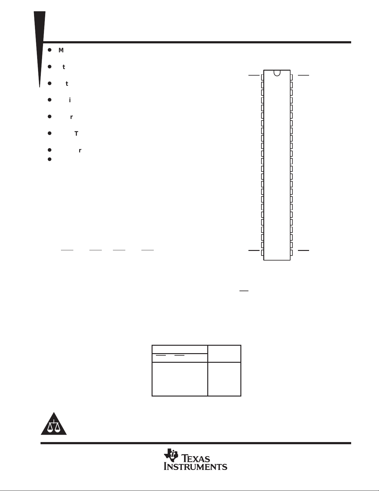
SN74ABT16541A . . . DGG, DGV, OR DL PACKAGE
SN54ABT16541 . . . WD PACKAGE
(TOP VIEW)
1
2
3
4
5
6
7
8
9
10
11
12
13
14
15
16
17
18
19
20
21
22
23
24
48
47
46
45
44
43
42
41
40
39
38
37
36
35
34
33
32
31
30
29
28
27
26
25
1OE2
1A1
1A2
GND
1A3
1A4
V
CC
1A5
1A6
GND
1A7
1A8
2A1
2A2
GND
2A3
2A4
V
CC
2A5
2A6
GND
2A7
2A8
2OE2
1OE1
1Y1
1Y2
GND
1Y3
1Y4
V
CC
1Y5
1Y6
GND
1Y7
1Y8
2Y1
2Y2
GND
2Y3
2Y4
V
CC
2Y5
2Y6
GND
2Y7
2Y8
2OE1
T o ensure the high-impedance state during power up or power down, OE
should be tied to VCC through a pullup
resistor; the minimum value of the resistor is determined by the current-sinking capability of the driver.
The SN54ABT16541 is characterized for operation over the full military temperature range of –55°C to 125°C.
The SN74ABT16541A is characterized for operation from –40°C to 85°C.
FUNCTION TABLE
(each 8-bit section)
INPUTS
OE1 OE2
L L L L
L LH H
H XX Z
X H X Z
Please be aware that an important notice concerning availability, standard warranty, and use in critical applications of
Texas Instruments semiconductor products and disclaimers thereto appears at the end of this data sheet.
Widebus and EPIC-ΙΙB are trademarks of Texas Instruments Incorporated.
UNLESS OTHERWISE NOTED this document contains PRODUCTION
DATA information current as of publication date. Products conform to
specifications per the terms of Texas Instruments standard warranty.
Production processing does not necessarily include testing of all
parameters.
POST OFFICE BOX 655303 • DALLAS, TEXAS 75265
OUTPUT
A
Y
Copyright 1997, Texas Instruments Incorporated
1
SN54ABT16541, SN74ABT16541A
16-BIT BUFFERS/DRIVERS
WITH 3-STATE OUTPUTS
SCBS118C – FEBRUAR Y 1991 – REVISED JANUAR Y 1997
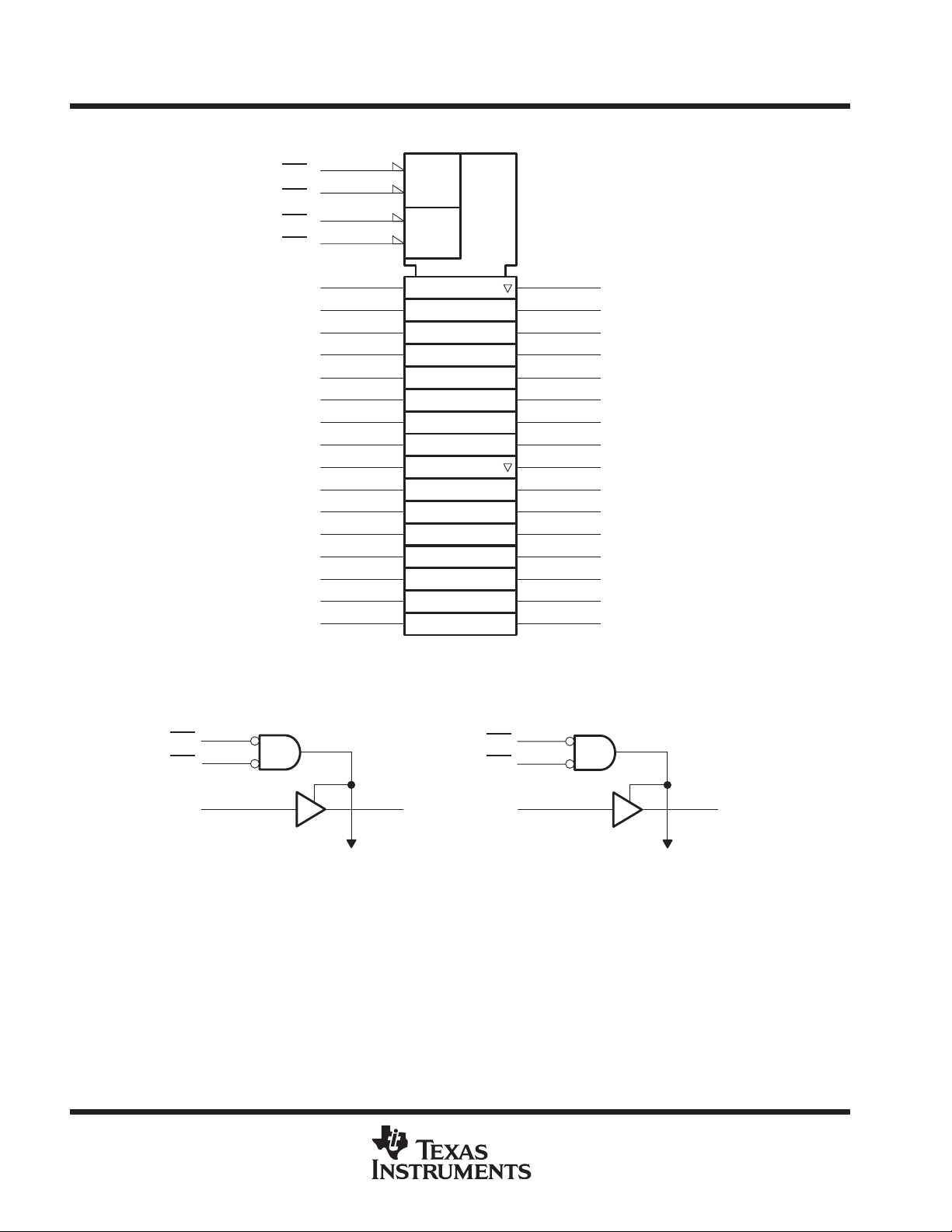
logic symbol
†
1OE1
1OE2
2OE1
2OE2
1
48
24
25
47
1A1
46
1A2
44
1A3 1Y3
43
1A4 1Y4
41
1A5 1Y5
40
1A6 1Y6
38
1A7 1Y7
37
1A8 1Y8
36
2A1 2Y1
35
2A2
33
2A3 2Y3
32
2A4 2Y4
30
2A5 2Y5
29
2A6 2Y6
27
2A7
26
2A8
&
&
EN1
EN2
111
2
1Y1
3
1Y2
5
6
8
9
11
12
2
13
14
16
17
19
20
22
23
2Y2
2Y7
2Y8
†
This symbol is in accordance with ANSI/IEEE Std 91-1984 and IEC Publication 617-12.
logic diagram (positive logic)
1
1OE1
48
1OE2
47
1A1 1Y1
To Seven Other Channels To Seven Other Channels
2
2OE1
2OE2
2A1
24
25
36
13
2Y1
2
POST OFFICE BOX 655303 • DALLAS, TEXAS 75265
 Loading...