

SN54ABT16470, SN74ABT16470
16-BIT REGISTERED TRANSCEIVERS
WITH 3-STATE OUTPUTS
SCBS085E – FEBRUARY 1991 – REVISED MAY 1997
1
POST OFFICE BOX 655303 • DALLAS, TEXAS 75265
D
Members of the Texas Instruments
Widebus
Family
D
State-of-the-Art
EPIC-ΙΙB
BiCMOS Design
Significantly Reduces Power Dissipation
D
Latch-Up Performance Exceeds 500 mA Per
JEDEC Standard JESD-17
D
T ypical V
OLP
(Output Ground Bounce) < 1 V
at VCC = 5 V, TA = 25°C
D
Distributed VCC and GND Pin Configuration
Minimizes High-Speed Switching Noise
D
Flow-Through Architecture Optimizes PCB
Layout
D
High-Drive Outputs (–32-mA IOH, 64-mA IOL)
D
Package Options Include Plastic 300-mil
Shrink Small-Outline (DL) and Thin Shrink
Small-Outline (DGG) Packages and 380-mil
Fine-Pitch Ceramic Flat (WD) Package
Using 25-mil Center-to-Center Spacings
description
The ’ABT16470 are 16-bit registered transceivers
that contain two sets of D-type flip-flops for
temporary storage of data flowing in either
direction. The ’ABT16470 can be used as two 8-bit
transceivers or one 16-bit transceiver. Separate
clock (CLKAB or CLKBA) and output-enable
(OEAB
or OEBA) inputs are provided for each
register to permit independent control in either
direction of data flow.
To avoid false clocking of the flip-flops, clock
enable (CLKEN) should not be switched from high
to low while CLK is high.
T o ensure the high-impedance state during power up or power down, OE should be tied to VCC through a pullup
resistor; the minimum value of the resistor is determined by the current-sinking capability of the driver.
The SN54ABT16470 is characterized for operation over the full military temperature range of –55°C to 125°C.
The SN74ABT16470 is characterized for operation from –40°C to 85°C.
Copyright 1997, Texas Instruments Incorporated
UNLESS OTHERWISE NOTED this document contains PRODUCTION
DATA information current as of publication date. Products conform to
specifications per the terms of Texas Instruments standard warranty.
Production processing does not necessarily include testing of all
parameters.
Please be aware that an important notice concerning availability, standard warranty, and use in critical applications of
Texas Instruments semiconductor products and disclaimers thereto appears at the end of this data sheet.
Widebus and EPIC-ΙΙB are trademarks of Texas Instruments Incorporated.
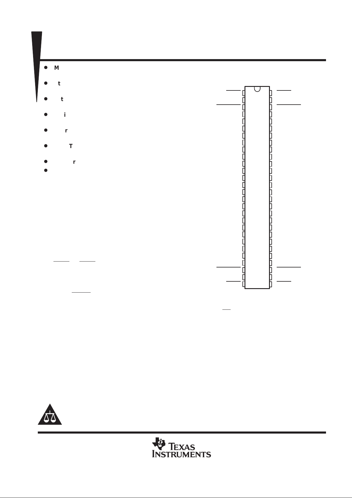
SN54ABT16470 . . . WD PACKAGE
SN74ABT16470 . . . DGG OR DL PACKAGE
(TOP VIEW)
1
2
3
4
5
6
7
8
9
10
11
12
13
14
15
16
17
18
19
20
21
22
23
24
25
26
27
28
56
55
54
53
52
51
50
49
48
47
46
45
44
43
42
41
40
39
38
37
36
35
34
33
32
31
30
29
1OEAB
1CLKAB
1CLKENAB
GND
1A1
1A2
V
CC
1A3
1A4
1A5
GND
1A6
1A7
1A8
2A1
2A2
2A3
GND
2A4
2A5
2A6
V
CC
2A7
2A8
GND
2CLKENAB
2CLKAB
2OEAB
1OEBA
1CLKBA
1CLKENBA
GND
1B1
1B2
V
CC
1B3
1B4
1B5
GND
1B6
1B7
1B8
2B1
2B2
2B3
GND
2B4
2B5
2B6
V
CC
2B7
2B8
GND
2CLKENBA
2CLKBA
2OEBA

SN54ABT16470, SN74ABT16470
16-BIT REGISTERED TRANSCEIVERS
WITH 3-STATE OUTPUTS
SCBS085E – FEBRUARY 1991 – REVISED MAY 1997
2
POST OFFICE BOX 655303 • DALLAS, TEXAS 75265
FUNCTION TABLE
†
INPUTS
OUTPUT
CLKENAB
CLKAB
OEAB
A
B
H X X X Z
X XHXZ
L LLXB
0
‡
L ↑ LL L
L ↑ L H H
†
A-to-B data flow is shown: B-to-A flow is similar but uses
CLKENBA
, CLKBA, and OEBA.
‡
Output level before the indicated steady-state input
conditions were established
SN54ABT16470, SN74ABT16470
16-BIT REGISTERED TRANSCEIVERS
WITH 3-STATE OUTPUTS
SCBS085E – FEBRUARY 1991 – REVISED MAY 1997
3
POST OFFICE BOX 655303 • DALLAS, TEXAS 75265
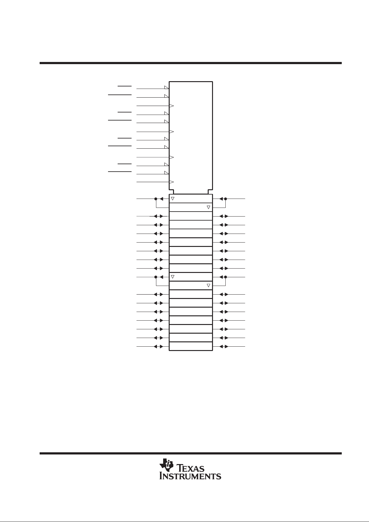
logic symbol
†
†
This symbol is in accordance with ANSI/IEEE Std 91-1984 and IEC Publication 617-12.
1OEBA
1CLKENBA
1OEAB
1CLKENAB
2OEBA
2CLKENBA
2OEAB
2CLKENAB
2
1CLKAB 2C6
1A1
5
6D
1A2
6
1A3
8
1A4
9
1A5
10
1A6
12
1A7
13
1A8
14
1B1
52
5D
1B2
51
1B3
49
1B4
48
1B5
47
1B6
45
1B7
44
1B8
43
2EN4
1
G2
3
30
2CLKBA
7C11
7EN9
29
G7
31
27
2CLKAB
8C12
8EN10
28
G8
26
55
1CLKBA
1C5
1EN3
56
G1
54
2A1
15
12D
2A2
16
2A3
17
2A4
19
2A5
20
2A6
21
2A7
23
2A8
24
2B1
42
11D
2B2
41
2B3
40
2B4
38
2B5
37
2B6
36
2B7
34
2B8
33
1
1
1
110
4
 Loading...