

Texas Instruments SN74ABT16374ADL, SN74ABT16374ADLR, SN74ABT16374ADGGR, SNJ54ABT16374AWD Datasheet
SN54ABT16374A, SN74ABT16374A
16-BIT EDGE-TRIGGERED D-TYPE FLIP-FLOPS
WITH 3-STATE OUTPUTS
SCBS205C – MARCH 1993 – REVISED MA Y 1997
D
Members of the Texas Instruments
Widebus
D
State-of-the-Art
Family
EPIC-ΙΙB
BiCMOS Design
Significantly Reduces Power Dissipation
D
ESD Protection Exceeds 2000 V Per
MIL-STD-883, Method 3015
D
Latch-Up Performance Exceeds 500 mA Per
JEDEC Standard JESD-17
D
Typical V
(Output Ground Bounce)
OLP
< 0.8 V at VCC = 5 V, TA = 25°C
D
High-Impedance State During Power Up
and Power Down
D
Distributed VCC and GND Pin Configuration
Minimizes High-Speed Switching Noise
D
Flow-Through Architecture Optimizes PCB
Layout
D
High-Drive Outputs (–32-mA IOH, 64-mA IOL)
D
Package Options Include Plastic 300-mil
Shrink Small-Outline (DL) and Thin Shrink
Small-Outline (DGG) Packages and 380-mil
Fine-Pitch Ceramic Flat (WD) Package
Using 25-mil Center-to-Center Spacings
description
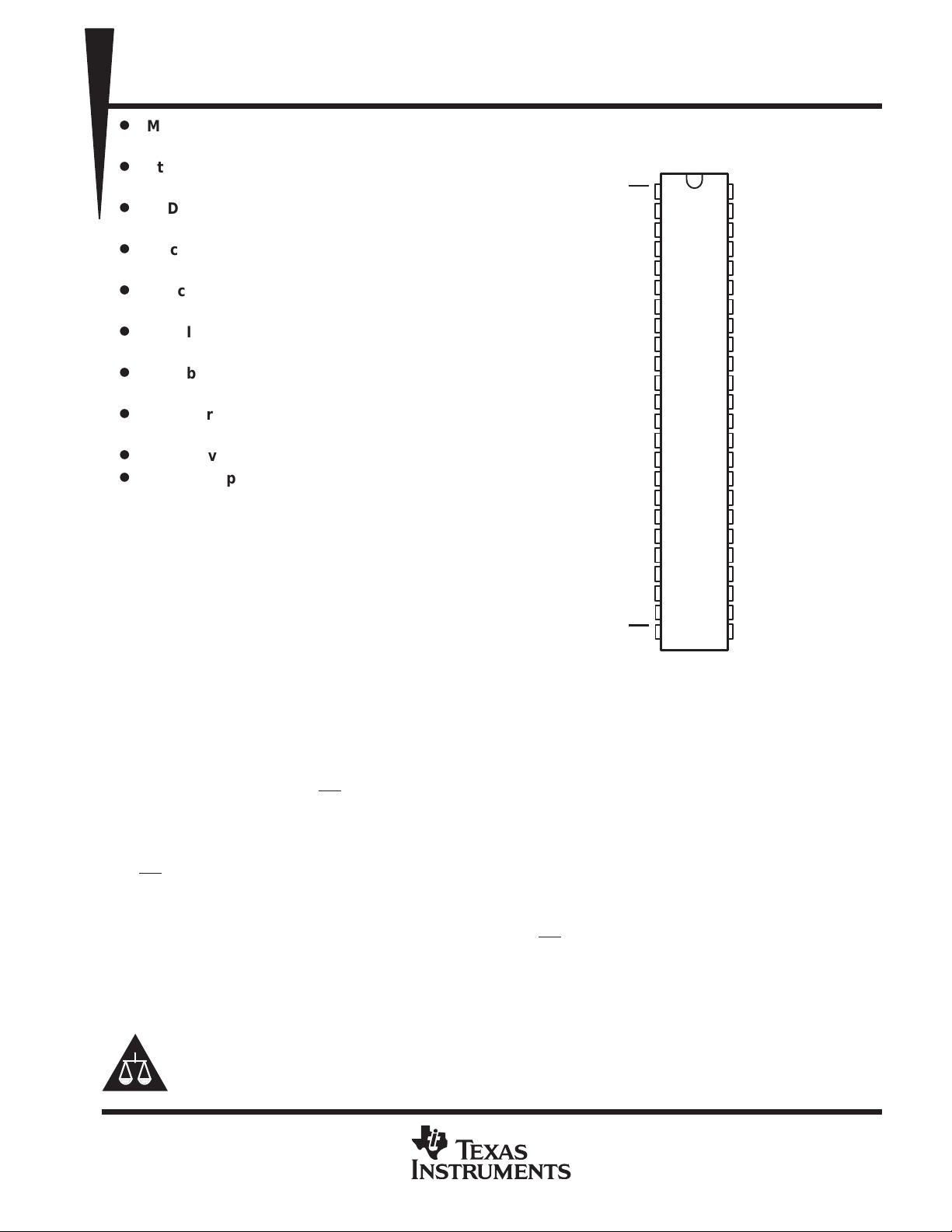
The ’ABT16374A are 16-bit edge-triggered
D-type flip-flops with 3-state outputs designed
SN54ABT16374A . . . WD PACKAGE
SN74ABT16374A . . . DGG OR DL PACKAGE
1OE
1Q1
1Q2
GND
1Q3
1Q4
V
CC
1Q5
1Q6
GND
1Q7
1Q8
2Q1
2Q2
GND
2Q3
2Q4
V
CC
2Q5
2Q6
GND
2Q7
2Q8
2OE
(TOP VIEW)
1
48
2
47
3
46
4
45
5
44
6
43
7
42
8
41
9
40
10
39
11
38
12
37
13
36
14
35
15
34
16
33
17
32
18
31
19
30
20
29
21
28
22
27
23
26
24
25
1CLK
1D1
1D2
GND
1D3
1D4
V
CC
1D5
1D6
GND
1D7
1D8
2D1
2D2
GND
2D3
2D4
V
CC
2D5
2D6
GND
2D7
2D8
2CLK
specifically for driving highly capacitive or
relatively low-impedance loads. They are
particularly suitable for implementing buffer
registers, I/O ports, bidirectional bus drivers, and
working registers.
These devices can be used as two 8-bit flip-flops or one 16-bit flip-flop. On the positive transition of the clock
(CLK) input, the Q outputs of the flip-flop take on the logic levels set up at the data (D) inputs.
A buffered output-enable (OE
) input can be used to place the eight outputs in either a normal logic state (high
or low logic levels) or a high-impedance state. In the high-impedance state, the outputs neither load nor drive
the bus lines significantly . The high-impedance state and the increased drive provide the capability to drive bus
lines without need for interface or pullup components
OE
does not affect internal operations of the flip-flop. Old data can be retained or new data can be entered while
the outputs are in the high-impedance state.
When VCC is between 0 and 2.1 V , the device is in the high-impedance state during power up or power down.
However, to ensure the high-impedance state above 2.1 V, OE
should be tied to VCC through a pullup resistor;
the minimum value of the resistor is determined by the current-sinking capability of the driver.
The SN54ABT16374A is characterized for operation over the full military temperature range of –55°C to 125°C.
The SN74ABT16374A is characterized for operation from –40°C to 85°C.
Please be aware that an important notice concerning availability, standard warranty, and use in critical applications of
Texas Instruments semiconductor products and disclaimers thereto appears at the end of this data sheet.
Widebus and EPIC-ΙΙB are trademarks of Texas Instruments Incorporated.
PRODUCTION DATA information is current as of publication date.
Products conform to specifications per the terms of Texas Instruments
standard warranty. Production processing does not necessarily include
testing of all parameters.
POST OFFICE BOX 655303 • DALLAS, TEXAS 75265
Copyright 1997, Texas Instruments Incorporated
1
SN54ABT16374A, SN74ABT16374A
16-BIT EDGE-TRIGGERED D-TYPE FLIP-FLOPS
WITH 3-STATE OUTPUTS
SCBS205C – MARCH 1993 – REVISED MA Y 1997
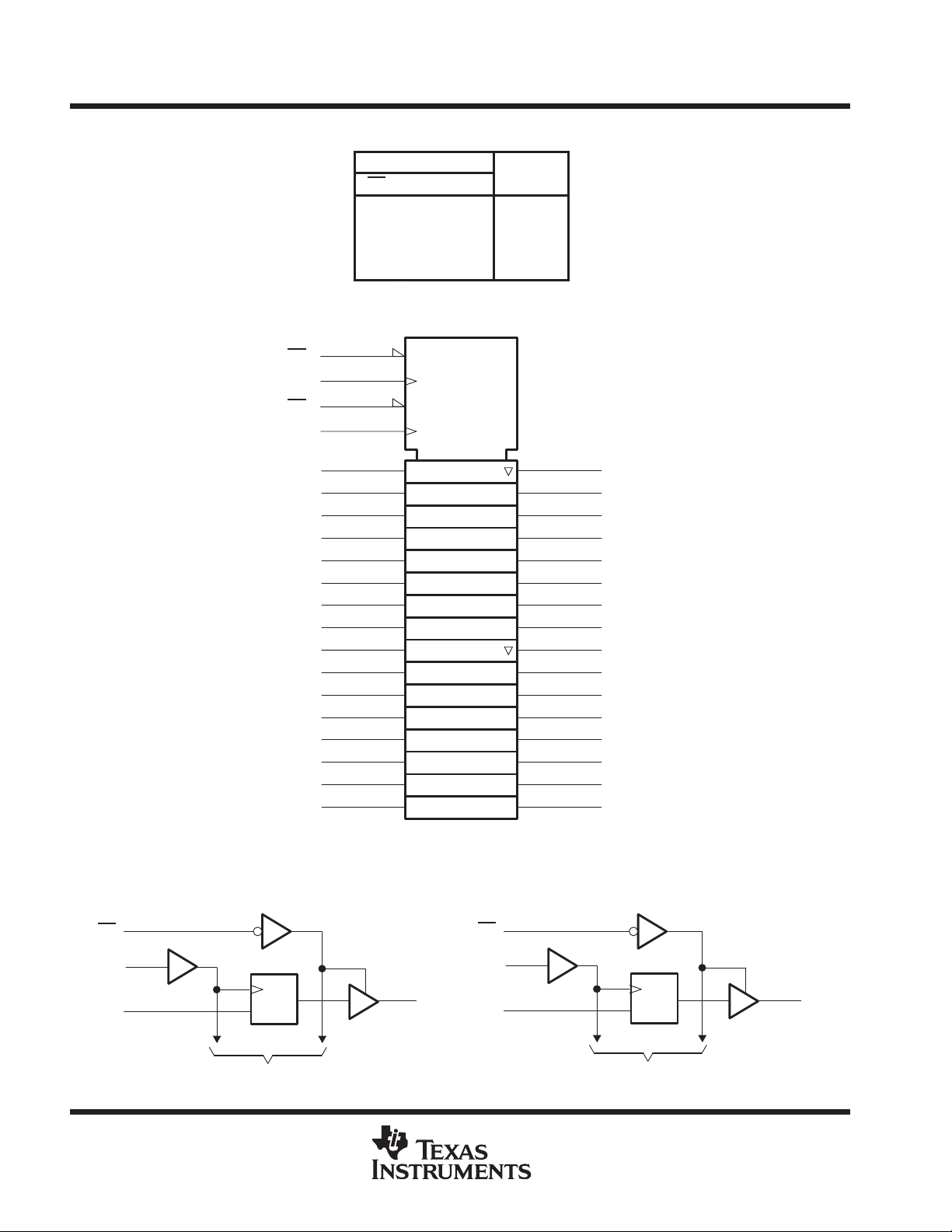
FUNCTION TABLE
(each flip-flop)
INPUTS
CLK D
OE
L ↑ H H
L ↑ LL
L H or L X Q
H X X Z
OUTPUT
Q
0
logic symbol
†
1D1
1D2
1D3
1D4
1D5
1D6
1D7
1D8
2D1
2D2
2D3
2D4
2D5
2D6
2D7
2D8
1
48
24
25
47
46
44
43
41
40
38
37
36
35
33
32
30
29
27
26
1EN
2EN
1D
2D
C1
C2
11
12
13
14
16
17
19
20
22
23
2
1Q1
3
1Q2
5
1Q3
6
1Q4
8
1Q5
9
1Q6
1Q7
1Q8
2Q1
2Q2
2Q3
2Q4
2Q5
2Q6
2Q7
2Q8
1
2
1OE
1CLK
2OE
2CLK
†
This symbol is in accordance with ANSI/IEEE Std 91-1984 and IEC Publication 617-12.
logic diagram (positive logic)
2
1OE
1CLK
1D1
1
48
47
C1
1D
To Seven Other Channels
2CLK
1Q1
POST OFFICE BOX 655303 • DALLAS, TEXAS 75265
2OE
2D1
24
25
36
C1
1D
To Seven Other Channels
132
2Q1
UNIT
SN54ABT16374A, SN74ABT16374A
16-BIT EDGE-TRIGGERED D-TYPE FLIP-FLOPS
WITH 3-STATE OUTPUTS
SCBS205C – MARCH 1993 – REVISED MA Y 1997
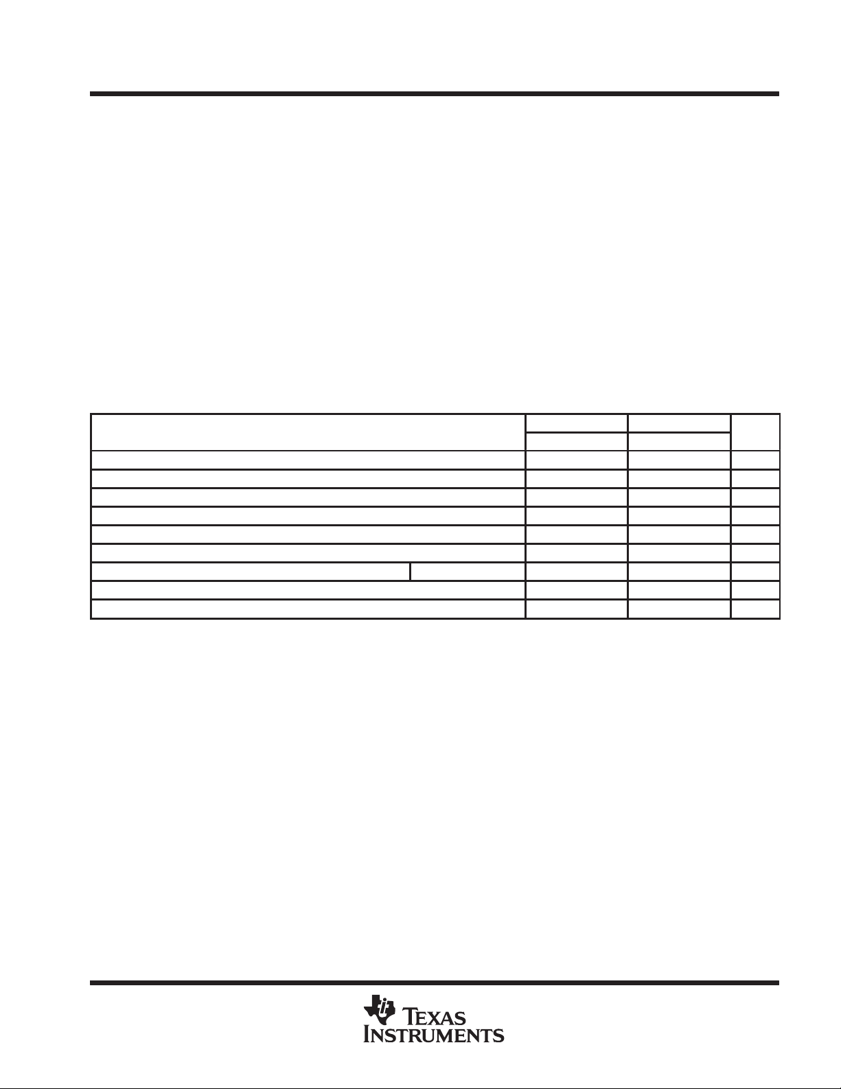
absolute maximum ratings over operating free-air temperature range (unless otherwise noted)
Supply voltage range, V
Input voltage range, VI (see Note 1) –0.5 V to 7 V. . . . . . . . . . . . . . . . . . . . . . . . . . . . . . . . . . . . . . . . . . . . . . . . . .
Voltage range applied to any output in the high or power-off state, VO –0.5 V to 5.5 V. . . . . . . . . . . . . . . . . . .
Current into any output in the low state, IO: SN54ABT16374A 96 mA. . . . . . . . . . . . . . . . . . . . . . . . . . . . . . . . .
Input clamp current, I
Output clamp current, I
Package thermal impedance, θJA (see Note 2): DGG package 89°C/W. . . . . . . . . . . . . . . . . . . . . . . . . . . . . . . .
Storage temperature range, T
†
Stresses beyond those listed under “absolute maximum ratings” may cause permanent damage to the device. These are stress ratings only, and
functional operation of the device at these or any other conditions beyond those indicated under “recommended operating conditions” is not
implied. Exposure to absolute-maximum-rated conditions for extended periods may affect device reliability.
NOTES: 1. The input and output negative-voltage ratings may be exceeded if the input and output clamp-current ratings are observed.
2. The package thermal impedance is calculated in accordance with EIA/JEDEC Std JESD51.
–0.5 V to 7 V. . . . . . . . . . . . . . . . . . . . . . . . . . . . . . . . . . . . . . . . . . . . . . . . . . . . . . . . . .
CC
SN74ABT16374A 128 mA. . . . . . . . . . . . . . . . . . . . . . . . . . . . . . . .
(V
< 0) –18 mA. . . . . . . . . . . . . . . . . . . . . . . . . . . . . . . . . . . . . . . . . . . . . . . . . . . . . . . . . . .
IK
I
(V
OK
< 0) –50 mA. . . . . . . . . . . . . . . . . . . . . . . . . . . . . . . . . . . . . . . . . . . . . . . . . . . . . . . .
O
DL package 94°C/W. . . . . . . . . . . . . . . . . . . . . . . . . . . . . . . . . .
–65°C to 150°C. . . . . . . . . . . . . . . . . . . . . . . . . . . . . . . . . . . . . . . . . . . . . . . . . . .
stg
recommended operating conditions (see Note 3)
SN54ABT16374A SN74ABT16374A
MIN MAX MIN MAX
V
CC
V
IH
V
IL
V
I
I
OH
I
OL
∆t/∆v Input transition rise or fall rate Outputs enabled 10 10 ns/V
∆t/∆V
T
A
NOTE 3: Unused inputs must be held high or low to prevent them from floating.
Supply voltage 4.5 5.5 4.5 5.5 V
High-level input voltage 2 2 V
Low-level input voltage 0.8 0.8 V
Input voltage 0 V
High-level output current –24 –32 mA
Low-level output current 48 64 mA
Power-up ramp rate 200 200 µs/V
CC
Operating free-air temperature –55 125 –40 85 °C
CC
0 V
CC
V
†
POST OFFICE BOX 655303 • DALLAS, TEXAS 75265
3
 Loading...