

Page 1

SN65LVDS33, SN65LVDT33, SN65LVDS34, SN65LVDT34
)
HIGH-SPEED DIFFERENTIAL RECEIVERS
SLLS490A – MARCH 2001 – REVISED MA Y 2001
D
400-Mbps Signaling Rate1 and 200-Mxfr/s
Data Transfer Rate
D
Operates With a Single 3.3-V Supply
D
–4-V to 5-V Common-Mode Input Voltage
Range
D
Differential Input Thresholds <±50 mV With
50 mV of Hysteresis Over Entire
Common-Mode Input Voltage Range
D
Integrated 110-Ω Line Termination
Resistors On LVDT Products
D
TSSOP Packaging (33 Only)
D
Complies With TIA/EIA-644 (LVDS)
D
Active Failsafe Assures a High-Level
Output With No Input
D
Bus-Pin ESD Protection Exceeds
15 kV HBM
D
Input Remains High-Impedance on Power
Down
D
TTL Inputs Are 5-V Tolerant
D
Pin-Compatible With the AM26LS32,
SN65LVDS32B, µA9637, SN65LVDS9637B
description
This family of four L VDS data line receivers offers
the widest common-mode input voltage range in
the industry. These receivers provide an input
voltage range specification compatible with a 5-V
PECL signal as well as an overall increased
ground-noise tolerance. They are in industry
standard footprints with integrated termination as
an option.
D OR PW PACKAGE
(TOP VIEW)
1B
1
16
1A
2
15
1Y
3
14
G
4
13
2Y
5
12
2A
6
11
7
2B
GND
V
CC
1Y
2Y
GND
D PACKAGE
(TOP VIEW)
10
8
1
2
3
4
SN65LVDS33D
SN65LVDT33D
SN65LVDS33PW
SN65LVDT33PW
V
CC
4B
4A
4Y
G
3Y
3A
9
3B
SN65LVDS34D
SN65LVDT34D
1A
8
1B
7
2A
6
2B
SN65LVDT34 ONLY
5
logic diagram (positive logic
G
G
SN65LVDT33 ONLY
1A
1B
2A
2B
3A
3B
4A
4B
1Y
2Y
3Y
4Y
logic diagram (positive logic)
1A
1B
2A
2B
1Y
2Y
Precise control of the differential input voltage
thresholds allows for inclusion of 50 mV of input
voltage hysteresis to improve noise rejection on
slowly changing input signals. The input thresholds are still no more than ±50 mV over the full
input common-mode voltage range.
The high-speed switching of L VDS signals usually
necessitates the use of a line impedance
matching resistor at the receiving-end of the cable
or transmission media. The SN65LVDT series of
receivers eliminates this external resistor by
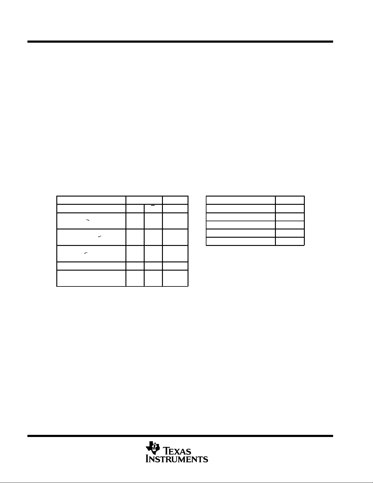
PART NUMBER
SN65LVDS33D
SN65LVDS33PW
SN65LVDT33D
SN65LVDT33PW
SN65LVDS34D
SN65LVDT34D
†
Add the suffix R for taped and reeled carrier .
AVAILABLE OPTIONS
NUMBER
†
OF
RECEIVERS
4
4
4
4
2
2
RESISTOR
No
No
Yes
Yes
No
Yes
SYMBOLIZATIONTERMINATION
LVDS33
LVDS33
LVDT33
LVDT33
LVDS34
LVDT34
integrating it with the receiver. The nonterminated
SN65LVDS series is also available for multidrop
or other termination circuits.
Please be aware that an important notice concerning availability, standard warranty, and use in critical applications of
Texas Instruments semiconductor products and disclaimers thereto appears at the end of this data sheet.
1
The signalling rate of a line, is the number of voltage transitions that are made per second expressed in the units bps (bits per second).
PRODUCTION DATA information is current as of publication date.
Products conform to specifications per the terms of Texas Instruments
standard warranty. Production processing does not necessarily include
testing of all parameters.
POST OFFICE BOX 655303 • DALLAS, TEXAS 75265
Copyright 2001, Texas Instruments Incorporated
1
Page 2
SN65LVDS33, SN65LVDT33, SN65LVDS34, SN65LVDT34
V
≥ -32 mV
100 mV
V
≤ –32 mV
VID≤ –100 mV
Open
HIGH-SPEED DIFFERENTIAL RECEIVERS
SLLS490A – MARCH 2001 – REVISED MAY 2001
description (continued)
The receivers can withstand ±15 kV human-body model (HBM) and ±600 V machine model (MM) electrostatic
discharges to the receiver input pins with respect to ground without damage. This provides reliability in cabled
and other connections where potentially damaging noise is always a threat.
The receivers also include a (patent pending) failsafe circuit that will provide a high-level output within 600 ns
after loss of the input signal. The most common causes of signal loss are disconnected cables, shorted lines,
or powered-down transmitters. The failsafe circuit prevents noise from being received as valid data under these
fault conditions. This feature may also be used for Wired-Or bus signaling. See The Active Failsafe Feature of
the SN65LVDS32B application note.
The intended application and signaling technique of these devices is point-to-point baseband data transmission
over controlled impedance media of approximately 100 Ω. The transmission media may be printed-circuit board
traces, backplanes, or cables. The ultimate rate and distance of data transfer is dependent upon the attenuation
characteristics of the media and the noise coupling to the environment.
The SN65L VDS33, SN65LVDT33, SN65LVDS34 and SN65L VDT34 are characterized for operation from –40°C
to 85°C.
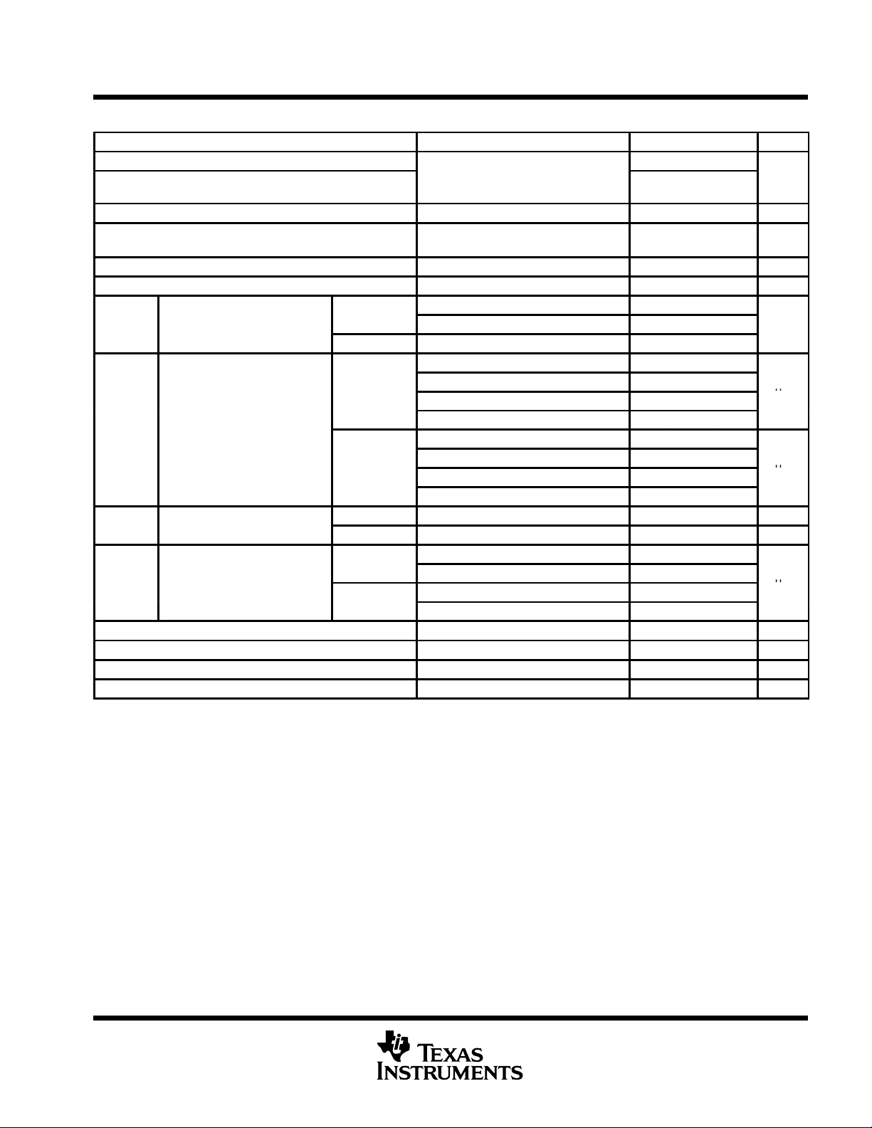
Function Tables
SN65LVDS33 and SN65LVDT33 SN65LVDS34 and SN65LVDT34
DIFFERENTIAL INPUT ENABLES OUTPUT DIFFERENTIAL INPUT OUTPUT
VID = VA – V
ID
–
H = high level, L = low level, X = irrelevant,
Z = high impedance (off), ? = indeterminate
<
B
ID
X L H Z
p
G G Y VID = VA – V
H X H
X L H
H X ?
X L ?
H X L
X L L
H X H
X L H
VID ≥ -32 mV H
–100 mV < VID ≤ –32 mV ?
VID≤ -100 mV L
Open H
H = high level, L = low level,
? = indeterminate
B
Y
2
POST OFFICE BOX 655303 • DALLAS, TEXAS 75265
Page 3

SN65LVDS33, SN65LVDT33, SN65LVDS34, SN65LVDT34
equivalent input and output schematic diagrams
Attenuation
Network
V
CC
1 pF
200 kΩ
3 pF
60 kΩ
250 kΩ
A Input
7 V
7 V
HIGH-SPEED DIFFERENTIAL RECEIVERS
SLLS490A – MARCH 2001 – REVISED MAY 2001
V
CC
6.5 kΩ 6.5 kΩ
Network
Attenuation
LVDT Only 110 Ω
Network
Attenuation
7 V
7 V
B Input
Enable
Inputs
(G Only)
7 V
300 kΩ
(G
Only)
100 Ω
300 kΩ
V
CC
V
CC
37 Ω
Y Output
7 V
POST OFFICE BOX 655303 • DALLAS, TEXAS 75265
3
Page 4

SN65LVDS33, SN65LVDT33, SN65LVDS34, SN65LVDT34
Magnitude of differential input voltage, VID
V
HIGH-SPEED DIFFERENTIAL RECEIVERS
SLLS490A – MARCH 2001 – REVISED MAY 2001
absolute maximum ratings over operating free-air temperature (unless otherwise noted)
Supply voltage range, V
(see Note 1) –0.5 V to 4 V. . . . . . . . . . . . . . . . . . . . . . . . . . . . . . . . . . . . . . . . . . . . . .
CC
†
Voltage range: Enables or Y –1 V to 6 V. . . . . . . . . . . . . . . . . . . . . . . . . . . . . . . . . . . . . . . . . . . . . . . . . . . . . . . . . .
A or B –5 V to 6 V. . . . . . . . . . . . . . . . . . . . . . . . . . . . . . . . . . . . . . . . . . . . . . . . . . . . . . . . . . . . . . . .
V
– VB (LVDT) 1 V. . . . . . . . . . . . . . . . . . . . . . . . . . . . . . . . . . . . . . . . . . . . . . . . . . . . . . . . . . . . .
A
Electrostatic discharge: A, B, and GND (see Note 2) Class 3, A: 15 kV, B: 600 V. . . . . . . . . . . . . . . . . . . . . . .
Charged-device mode: All pins (see Note 3) ±500 V. . . . . . . . . . . . . . . . . . . . . . . . . . . . . . . . . . . . . . . . . . . . . . .
Continuous power dissipation See Dissipation Rating Table. . . . . . . . . . . . . . . . . . . . . . . . . . . . . . . . . . . . . . . . .
Storage temperature range –65°C to 150°C. . . . . . . . . . . . . . . . . . . . . . . . . . . . . . . . . . . . . . . . . . . . . . . . . . . . . . . .
Lead temperature 1,6 mm (1/16 inch) from case for 10 seconds 260°C. . . . . . . . . . . . . . . . . . . . . . . . . . . . . . .
†
Stresses beyond those listed under “absolute maximum ratings” may cause permanent damage to the device. These are stress ratings only, and
functional operation of the device at these or any other conditions beyond those indicated under “recommended operating conditions” is not
implied. Exposure to absolute-maximum-rated conditions for extended periods may affect device reliability.
NOTES: 1. All voltage values, except dif ferential I/O bus voltages, are with respect to network ground terminal.
2. Tested in accordance with JEDEC Standard 22, Test Method A114-A.
3. Tested in accordance with JEDEC Standard 22, Test Method C101.
DISSIPATION RATING TABLE
PACKAGE
D8 725 mW 5.8 mW/°C 377 mW
PW16 774 mW 6.2 mW/°C 402 mW
D16 950 mW 7.6 mW/°C 494 mW
‡
This is the inverse of the junction-to-ambient thermal resistance when board-mounted and with
no air flow.
TA ≤ 25°C
POWER RATING
OPERATING FACTOR
ABOVE TA = 25°C
‡
TA = 85°C
POWER RATING
recommended operating conditions
Supply voltage, V
High-level input voltage, V
Low-level input voltage, V
Voltage at any bus terminal (separately or common-mode), VI or V
Operating free-air temperature, T
CC
IH
IL
p
A
Enables 2 5 V
Enables 0 0.8 V
LVDS 0.1 3
LVDT 0.8
MIN NOM MAX UNIT
3 3.3 3.6 V
IC
–4 5 V
–40 85 °C
4
POST OFFICE BOX 655303 • DALLAS, TEXAS 75265
Page 5
SN65LVDS33, SN65LVDT33, SN65LVDS34, SN65LVDT34
SN65LVDx33
SN65LVDS
A
IIInput current (A or B inputs)
SN65LVDT
A
I
SN65LVDS
I
A
SN65LVDT
HIGH-SPEED DIFFERENTIAL RECEIVERS
SLLS490A – MARCH 2001 – REVISED MAY 2001
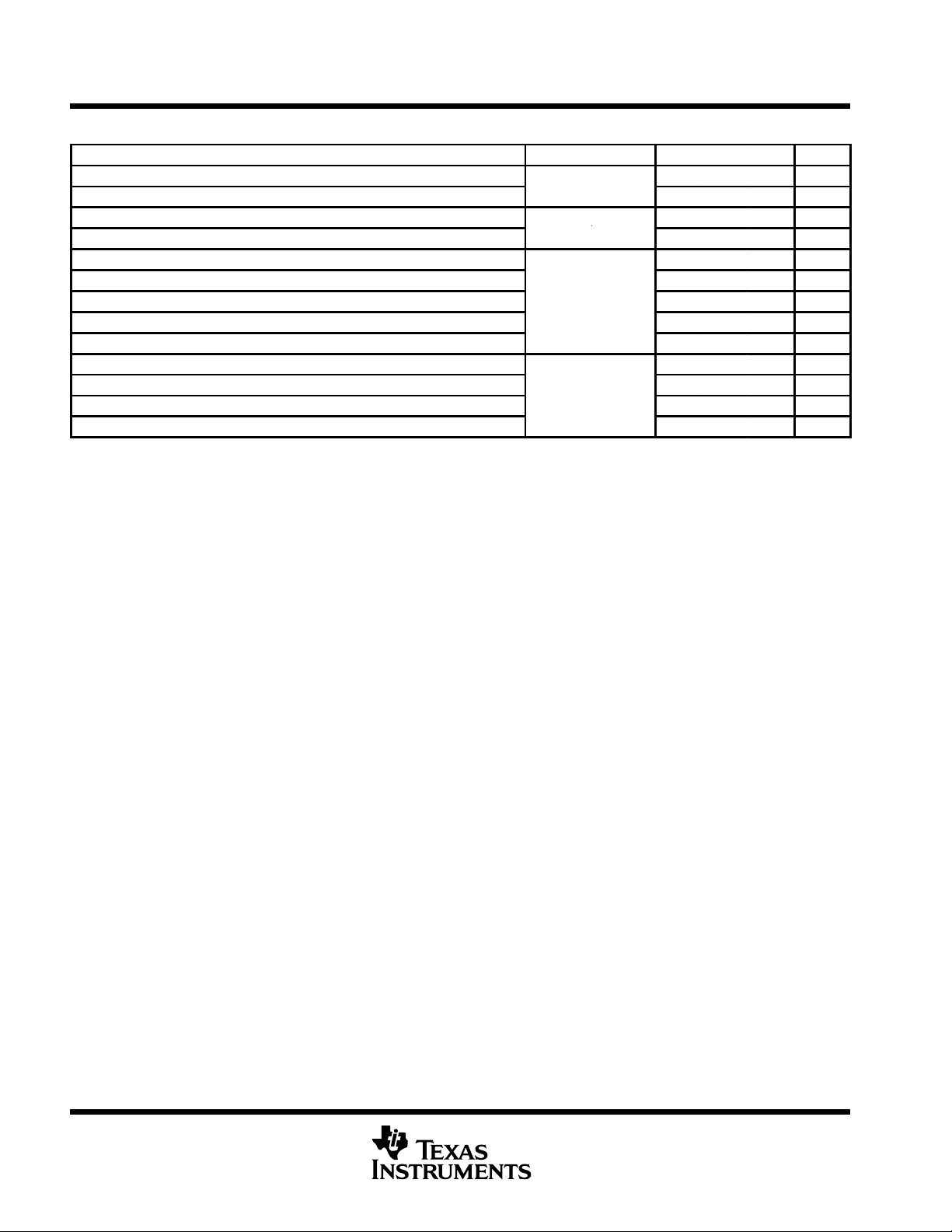
electrical characteristics over recommended operating conditions (unless otherwise noted)
PARAMETER TEST CONDITIONS MIN TYP†MAX UNIT
V
IT1
V
IT2
V
IT3
V
ID(HYS)
V
OH
V
OL
I
CC
ID
I(OFF)
I
IH
I
IL
I
OZ
C
I
†
All typical values are at 25°C and with a 3.3 V supply.
Positive-going differential input voltage threshold 50
Negative-going differential input voltage
threshold
Differential input failsafe voltage threshold See Table 1 and Figure 5 –32 –100 mV
Differential input voltage hysteresis,
V
– V
IT1
IT2
High-level output voltage IOH = –4 mA 2.4 V
Low-level output voltage IOL = 4 mA 0.4 V
Supply current
SN65LVDx34 No load, Steady-state 8 12
p
Differential input current
(IIA – IIB)
Power-off input current
(A or B inputs)
High-level input current (enables) VIH = 2 V 10 µA
Low-level input current (enables) VIL = 0.8 V 10 µA
High-impedance output current –10 10 µA
Input capacitance, A or B input to GND VI = 0.4 sin (4E6πt) + 0.5 V 5 pF
p
SN65LVDS VID = 100 mV, VIC= –4 V or 5 V ±3 µA
SN65LVDT VID = 200 mV, VIC= –4 V or 5 V 1.55 2.22 mA
VIB = –4 V or 5 V, See Figures 1 and 2
G at VCC, No load, Steady-state 16 23
G at GND 1.1 5
VI = 0 V, Other input open ±20
VI = 2.4 V, Other input open ±20
VI = –4 V, Other input open ±75
VI = 5 V, Other input open ±40
VI = 0 V, Other input open ±40
VI = 2.4 V, Other input open ±40
VI = –4 V, Other input open ±150
VI = 5 V, Other input open ±80
VA or VB = 0 V or 2.4 V, VCC = 0 V ±20
VA or VB = –4 or 5 V, VCC = 0 V ±50
VA or VB =0 V or 2.4 V, VCC = 0 V ±30
VA or VB = –4 V or 5 V, VCC = 0 V ±100
–50
50 mV
mV
mA
µ
µ
µ
POST OFFICE BOX 655303 • DALLAS, TEXAS 75265
5
Page 6
SN65LVDS33, SN65LVDT33, SN65LVDS34, SN65LVDT34
See Figure 3
L
,
See Figure 4
HIGH-SPEED DIFFERENTIAL RECEIVERS
SLLS490A – MARCH 2001 – REVISED MAY 2001
switching characteristics over recommended operating conditions (unless otherwise noted)
PARAMETER TEST CONDITIONS MIN TYP†MAX UNIT
t
PLH(1)
t
PHL(1)
t
d1
t
d2
t
sk(p)
t
sk(o)
t
sk(pp)
t
r
t
f
t
PHZ
t
PLZ
t
PZH
t
PZL
†
All typical values are at 25°C and with a 3.3-V supply.
‡
t
sk(o)
§
t
sk(pp)
operate with the same supply voltages, at the same temperature, and have identical packages and test circuits.
Propagation delay time, low-to-high-level output
Propagation delay time, high-to-low-level output
Delay time, failsafe deactivate time
Delay time, failsafe activate time
Pulse skew (|t
Output skew
Part-to-part skew
Output signal rise time 0.8 ns
Output signal fall time 0.8 ns
Propagation delay time, high-level-to-high-impedance output 5.5 9 ns
Propagation delay time, low-level-to-high-impedance output
Propagation delay time, high-impedance -to-high-level output
Propagation delay time, high-impedance-to-low-level output 7 9 ns
is the magnitude of the time difference between the t
is the magnitude of the time difference in propagation delay times between any specified terminals of two devices when both devices
‡
PHL(1)
§
– t
|) 200 ps
PLH(1)
or t
PLH
of all receivers of a single device with all of their inputs driven together.
PHL
C
= 10 pF,
See Figures 3 and 6
See Figure 3
2.5 4 6 ns
2.5 4 6 ns
9 ns
0.3 1.5 µs
150 ps
1 ns
4.4 9 ns
3.8 9 ns
6
POST OFFICE BOX 655303 • DALLAS, TEXAS 75265
Page 7

SN65LVDS33, SN65LVDT33, SN65LVDS34, SN65LVDT34
HIGH-SPEED DIFFERENTIAL RECEIVERS
PARAMETER MEASUREMENT INFORMATION
I
(VIA + VIB)/2
IA
V
IA
V
IC
I
IB
V
IB
Figure 1. Voltage and Current Definitions
1000 Ω
†
100 Ω
100 Ω
V
ID
A
V
ID
B
SLLS490A – MARCH 2001 – REVISED MAY 2001
V
Y
O
V
O
IT1
1000 Ω
and V
Input Voltage Threshold Test Circuit and Definitions
IT2
+
V
IC
–
†
Remove for testing LVDT device.
V
ID
V
O
V
ID
V
O
NOTE: Input signal of 3 Mpps, duration of 167 ns, and transition time of <1 ns.
Figure 2. V
10 pF,
2 Places
10 pF
V
O
V
IT1
0 V
–100 mV
100 mV
0 V
V
IT2
POST OFFICE BOX 655303 • DALLAS, TEXAS 75265
7
Page 8

SN65LVDS33, SN65LVDT33, SN65LVDS34, SN65LVDT34
HIGH-SPEED DIFFERENTIAL RECEIVERS
SLLS490A – MARCH 2001 – REVISED MAY 2001
PARAMETER MEASUREMENT INFORMATION
V
ID
V
IA
V
IB
CL = 10 pF
V
O
V
IA
V
IB
V
ID
t
PHL
V
O
NOTE: All input pulses are supplied by a generator having the following characteristics: tr or tf ≤ 1 ns, pulse repetition rate (PRR) = 50 Mpps,
pulsewidth = 10 ±0.2 ns . CL includes instrumentation and fixture capacitance within 0,06 mm of the D.U.T.
80%
20%
t
f
80%
20%
t
PLH
1.4 V
1 V
0.4 V
0 V
–0.4 V
V
OH
1.4 V
V
OL
t
r
Figure 3. Timing Test Circuit and Waveforms
8
POST OFFICE BOX 655303 • DALLAS, TEXAS 75265
Page 9

SN65LVDS33, SN65LVDT33, SN65LVDS34, SN65LVDT34
HIGH-SPEED DIFFERENTIAL RECEIVERS
SLLS490A – MARCH 2001 – REVISED MAY 2001
PARAMETER MEASUREMENT INFORMATION
1.2 V
Inputs
NOTE: All input pulses are supplied by a generator having the following characteristics: tr or tf ≤ 1 ns, pulse
repetition rate (PRR) = 0.5 Mpps, pulsewidth = 500 ±10 ns . CL includes instrumentation and fixture
capacitance within 0,06 mm of the D.U.T.
V
TEST
A
G
G
t
PZL
Y
V
TEST
A
G
G
t
PZH
Y
t
PLZ
t
PHZ
G
G
B
500 Ω
A
10 pF
t
t
PZL
PZH
V
O
t
PLZ
t
PHZ
±
2.5 V
1 V
2 V
1.4 V
0.8 V
2 V
1.4 V
0.8 V
2.5 V
1.4 V
VOL +0.5 V
V
OL
0
1.4 V
2 V
1.4 V
0.8 V
2 V
1.4 V
0.8 V
V
OH
VOH –0.5 V
1.4 V
0
V
TEST
Figure 4. Enable/Disable Time Test Circuit and Waveforms
POST OFFICE BOX 655303 • DALLAS, TEXAS 75265
9
Page 10

SN65LVDS33, SN65LVDT33, SN65LVDS34, SN65LVDT34
HIGH-SPEED DIFFERENTIAL RECEIVERS
SLLS490A – MARCH 2001 – REVISED MAY 2001
PARAMETER MEASUREMENT INFORMATION
Table 1. Receiver Minimum and Maximum V
IT3
Input Threshold Test Voltages
APPLIED VOLTAGES
VIA (mV) VIB (mV) VID (mV) VIC (mV) Output
–4000 –3900 –100 –3950 L
–4000 –3968 –32 –3984 H
4900 5000 –100 4950 L
4968 5000 –32 4984 H
†
These voltages are applied for a minimum of 1.5 µs.
V
IA
V
IB
V
O
V
IA
V
IB
V
O
†
RESULTANT INPUTS
a) No Failsafe
–100 mV @ 250 KHz
–32 mV @ 250 KHz
Failsafe Asserted
b) Failsafe Asserted
1.4 V
1 V
0.4 V
0 V
–0.4 V
V
OH
1.4 V
V
OL
Figure 5. V
Failsafe Threshold Test
IT3
>1.5 µs
t
d1
–0.2 V
t
d2
Figure 6. Waveforms for Failsafe Activate and Deactivate
10
POST OFFICE BOX 655303 • DALLAS, TEXAS 75265
Page 11

SN65LVDS33, SN65LVDT33, SN65LVDS34, SN65LVDT34
HIGH-SPEED DIFFERENTIAL RECEIVERS
SLLS490A – MARCH 2001 – REVISED MAY 2001
TYPICAL CHARACTERISTICS
LOW-LEVEL OUTPUT VOLTAGE
vs
LOW-LEVEL OUTPUT CURRENT
5
VCC = 3.3 V
TA = 25°C
4
3
2
– Low-Level Output Voltage – V
1
OL
V
0
0
10
IOL – Low-Level Output Current – mA
20 30
Figure 7
LOW-TO-HIGH PROPAGATION DELAY TIME
vs
FREE-AIR TEMPERATURE
5
40
– High-Level Output Voltage – V
V
HIGH-LEVEL OUTPUT VOLTAGE
vs
HIGH-LEVEL OUTPUT CURRENT
4
VCC = 3.3 V
TA = 25°C
3
2
1
OH
0
–30 –20–40
IOH – High-Level Output Current – mA
Figure 8
HIGH-TO-LOW PROPAGATION DELAY TIME
vs
FREE-AIR TEMPERATURE
5
0–10
4.5
VCC = 3 V
4
3.5
– Low-To-High Propagation Delay T ime – ns
PLH
t
3
–50 0 50
VCC = 3.3 V
TA – Free-Air Temperature – °C
Figure 9
VCC = 3.6 V
POST OFFICE BOX 655303 • DALLAS, TEXAS 75265
100
4.5
VCC = 3 V
4
3.5
– High-To-Low Propagation Delay T ime – ns
PHL
t
3
–50 0 50
VCC = 3.3 V
TA – Free-Air Temperature – °C
Figure 10
VCC = 3.6 V
100
11
Page 12

SN65LVDS33, SN65LVDT33, SN65LVDS34, SN65LVDT34
HIGH-SPEED DIFFERENTIAL RECEIVERS
SLLS490A – MARCH 2001 – REVISED MAY 2001
TYPICAL CHARACTERISTICS
SUPPLY CURRENT
vs
FREQUENCY
140
120
100
80
60
40
– Supply Current – mAI
CC
20
0
0 100
VCC = 3.3 V
VCC = 3.6 V
VCC = 3 V
150 200
f – Switching Frequency – MHz
Figure 11
12
POST OFFICE BOX 655303 • DALLAS, TEXAS 75265
Page 13

SN65LVDS33, SN65LVDT33, SN65LVDS34, SN65LVDT34
HIGH-SPEED DIFFERENTIAL RECEIVERS
SLLS490A – MARCH 2001 – REVISED MAY 2001
APPLICATION INFORMATION
0.01 µF
16
V
1
1B
100 Ω
100 Ω
NOTES: A. Place a 0.1-µF Z5U ceramic, mica or polystyrene dielectric, 0805 size, chip capacitor between VCC and the ground plane. The
capacitor should be located as close as possible to the device terminals.
B. The termination resistance value should match the nominal characteristic impedance of the transmission media with ±10%.
C. Unused enable inputs should be tied to VCC or GND as appropriate.
2
1A
3
1Y
4
V
CC
G
5
2Y
6
2A
7
2B
8
GND
CC
4B
4A
4Y
3Y
3A
3B
15
14
13
12
G
11
10
9
≈3.6 V
0.1 µF
(see Note A)
100 Ω
(see Note B)
See Note C
100 Ω
5 V
1N645
(2 places)
Figure 12. Operation With 5-V Supply
related information
IBIS modeling is available for this device. Please contact the local TI sales office or the TI Web site at www.ti.com
for more information.
For more application guidelines, please see the following documents:
D
Low-Voltage Differential Signalling Design Notes (TI literature number SLLA014)
D
Interface Circuits for TIA/EIA-644 (LVDS) (SLLA038)
D
Reducing EMI With L VDS (SLLA030)
D
Slew Rate Control of LVDS Circuits (SLLA034)
D
Using an LVDS Receiver With RS-422 Data (SLLA031)
D
Evaluating the LVDS EVM (SLLA033)
POST OFFICE BOX 655303 • DALLAS, TEXAS 75265
13
Page 14

SN65LVDS33, SN65LVDT33, SN65LVDS34, SN65LVDT34
HIGH-SPEED DIFFERENTIAL RECEIVERS
SLLS490A – MARCH 2001 – REVISED MAY 2001
APPLICATION INFORMATION
active failsafe feature
A differential line receiver commonly has a failsafe circuit to prevent it from switching on input noise. Current
LVDS failsafe solutions require either external components with subsequent reductions in signal quality or
integrated solutions with limited application. This family of receivers has a new integrated failsafe that solves
the limitations seen in present solutions. A detailed theory of operation is presented in application note The
Active Failsafe Feature of the SN65LVDS32B, literature number SLLA082A.
The following figure shows one receiver channel with active failsafe. It consists of a main receiver that can
respond to a high-speed input differential signal. Also connected to the input pair are two failsafe receivers that
form a window comparator. The window comparator has a much slower response than the main receiver and
it detects when the input differential falls below 80 mV. A 600-ns failsafe timer filters the window comparator
outputs. When failsafe is asserted, the failsafe logic drives the main receiver output to logic high.
Main Receiver
A
B
+
_
Failsafe
Reset
Timer
Output
Buffer
R
A > B + 80 mV
+
_
B > A + 80 mV
+
_
Window Comparator
Figure 13. Receiver With Active Failsafe
Failsafe
14
POST OFFICE BOX 655303 • DALLAS, TEXAS 75265
Page 15

SN65LVDS33, SN65LVDT33, SN65LVDS34, SN65LVDT34
HIGH-SPEED DIFFERENTIAL RECEIVERS
SLLS490A – MARCH 2001 – REVISED MAY 2001
APPLICATION INFORMATION
ECL/PECL-to-LVTTL conversion with TI’s LVDS receiver
The various versions of emitter-coupled logic (i.e. ECL, PECL and LVPECL) are often the physical layer of
choice for system designers. Designers know of the established technology and that it is capable of high-speed
data transmission. In the past, system requirements often forced the selection of ECL. Now technologies like
L VDS provide designers with another alternative. While the total exchange of ECL for LVDS may not be a design
option, designers have been able to take advantage of L VDS by implementing a small resistor divider network
at the input of the L VDS receiver. TI has taken the next step by introducing a wide common-mode L VDS receiver
(no divider network required) which can be connected directly to an ECL driver with only the termination bias
voltage required for ECL termination (V
Figures 14 and 15 show the use of an L V/PECL driver driving 5 meters of CAT–5 cable and being received by
TI’s wide common-mode receiver and the resulting eye-pattern. The values for R3 are required in order to
provide a resistor path to ground for the L V/PECL driver . With no resistor divider , R1 simply needs to match the
characteristic load impedance of 50 Ω. The R2 resistor is a small value and is intended to minimize any possible
common-mode current reflections.
CC
– 2 V).
V
CC
I
CC
V
EE
R3 = 240 Ω
R3 R3
5 Meters
of CAT-5
R1 = 50 Ω
R2 = 50 Ω
V
B
V
B
R1 R1
R2
V
CC
I
CC
LVDSLV/PECL
Figure 14. L VPECL or PECL to Remote Wide Common-Mode L VDS Receiver
Figure 15. LV/PECL to Remote SN65L VDS33 at 500 Mbps Receiver Output (CH1)
POST OFFICE BOX 655303 • DALLAS, TEXAS 75265
15
Page 16

SN65LVDS33, SN65LVDT33, SN65LVDS34, SN65LVDT34
HIGH-SPEED DIFFERENTIAL RECEIVERS
SLLS490A – MARCH 2001 – REVISED MAY 2001
APPLICATION INFORMATION
test conditions
D
VCC = 3.3 V
D
TA = 25°C (ambient temperature)
D
All four channels switching simultaneously with NRZ data. Scope is pulse-triggered simultaneously with
NRZ data.
equipment
D
Tektronix PS25216 programmable power supply
D
Tektronix HFS 9003 stimulus system
D
Tektronix TDS 784D 4-channel digital phosphor oscilloscope – DPO
Tektronix PS25216
Programmable
Power Supply
Tektronix HFS 9003
Stimulus System
Bench Test Board
Figure 16. Equipment Setup
Trigger
Tektronix TDS 784D 4-Channel
Digital Phosphor
Oscilloscope – DPO
16
100 Mbit/s 200 Mbit/s
Figure 17. T ypical Eye Pattern SN65LVDS33
POST OFFICE BOX 655303 • DALLAS, TEXAS 75265
Page 17

SN65LVDS33, SN65LVDT33, SN65LVDS34, SN65LVDT34
HIGH-SPEED DIFFERENTIAL RECEIVERS
SLLS490A – MARCH 2001 – REVISED MAY 2001
MECHANICAL DATA
D (R-PDSO-G**) PLASTIC SMALL-OUTLINE PACKAGE
14 PIN SHOWN
0.050 (1,27)
14
1
0.069 (1,75) MAX
0.020 (0,51)
0.014 (0,35)
8
7
A
0.010 (0,25)
0.004 (0,10)
DIM
0.157 (4,00)
0.150 (3,81)
PINS **
0.010 (0,25)
0.244 (6,20)
0.228 (5,80)
8
M
Seating Plane
0.004 (0,10)
14
0.008 (0,20) NOM
0°–8°
16
Gage Plane
0.010 (0,25)
0.044 (1,12)
0.016 (0,40)
A MAX
A MIN
NOTES: A. All linear dimensions are in inches (millimeters).
B. This drawing is subject to change without notice.
C. Body dimensions do not include mold flash or protrusion, not to exceed 0.006 (0,15).
POST OFFICE BOX 655303 • DALLAS, TEXAS 75265
0.197
(5,00)
0.189
(4,80)
0.344
(8,75)
0.337
(8,55)
0.394
(10,00)
0.386
(9,80)
4040047/D 10/96
17
Page 18

SN65LVDS33, SN65LVDT33, SN65LVDS34, SN65LVDT34
HIGH-SPEED DIFFERENTIAL RECEIVERS
SLLS490A – MARCH 2001 – REVISED MAY 2001
MECHANICAL DATA
PW (R-PDSO-G**) PLASTIC SMALL-OUTLINE PACKAGE
14 PINS SHOWN
0,65
1,20 MAX
14
0,30
0,19
8
4,50
4,30
PINS **
7
Seating Plane
0,15
0,05
8
1
A
DIM
6,60
6,20
14
0,10
M
0,10
2016
0,15 NOM
0°–8°
24
Gage Plane
0,25
0,75
0,50
28
A MAX
A MIN
NOTES: A. All linear dimensions are in millimeters.
B. This drawing is subject to change without notice.
C. Body dimensions do not include mold flash or protrusion not to exceed 0,15.
D. Falls within JEDEC MO-153
3,10
2,90
5,10
4,90
5,10
4,90
6,60
6,40
7,90
7,70
9,80
9,60
4040064/F 01/97
18
POST OFFICE BOX 655303 • DALLAS, TEXAS 75265
Page 19

IMPORTANT NOTICE
T exas Instruments and its subsidiaries (TI) reserve the right to make changes to their products or to discontinue
any product or service without notice, and advise customers to obtain the latest version of relevant information
to verify, before placing orders, that information being relied on is current and complete. All products are sold
subject to the terms and conditions of sale supplied at the time of order acknowledgment, including those
pertaining to warranty, patent infringement, and limitation of liability.
TI warrants performance of its products to the specifications applicable at the time of sale in accordance with
TI’s standard warranty . T esting and other quality control techniques are utilized to the extent TI deems necessary
to support this warranty . Specific testing of all parameters of each device is not necessarily performed, except
those mandated by government requirements.
Customers are responsible for their applications using TI components.
In order to minimize risks associated with the customer’s applications, adequate design and operating
safeguards must be provided by the customer to minimize inherent or procedural hazards.
TI assumes no liability for applications assistance or customer product design. TI does not warrant or represent
that any license, either express or implied, is granted under any patent right, copyright, mask work right, or other
intellectual property right of TI covering or relating to any combination, machine, or process in which such
products or services might be or are used. TI’s publication of information regarding any third party’s products
or services does not constitute TI’s approval, license, warranty or endorsement thereof.
Reproduction of information in TI data books or data sheets is permissible only if reproduction is without
alteration and is accompanied by all associated warranties, conditions, limitations and notices. Representation
or reproduction of this information with alteration voids all warranties provided for an associated TI product or
service, is an unfair and deceptive business practice, and TI is not responsible nor liable for any such use.
Resale of TI’s products or services with
that product or service voids all express and any implied warranties for the associated TI product or service,
is an unfair and deceptive business practice, and TI is not responsible nor liable for any such use.
Also see: Standard T erms and Conditions of Sale for Semiconductor Products.
Copyright 2001, Texas Instruments Incorporated
statements different from or beyond the parameters
www.ti.com/sc/docs/stdterms.htm
Mailing Address:
Texas Instruments
Post Office Box 655303
Dallas, Texas 75265
stated by TI for
 Loading...