

www.ti.com
Flatlink 3Gä
1
4
7
*
3
6
9
#
2
5
8
0
Application
Processor
with
RGB
Video
Interface
LVDS304
LVDS303
LCD
Driver
DATACLK
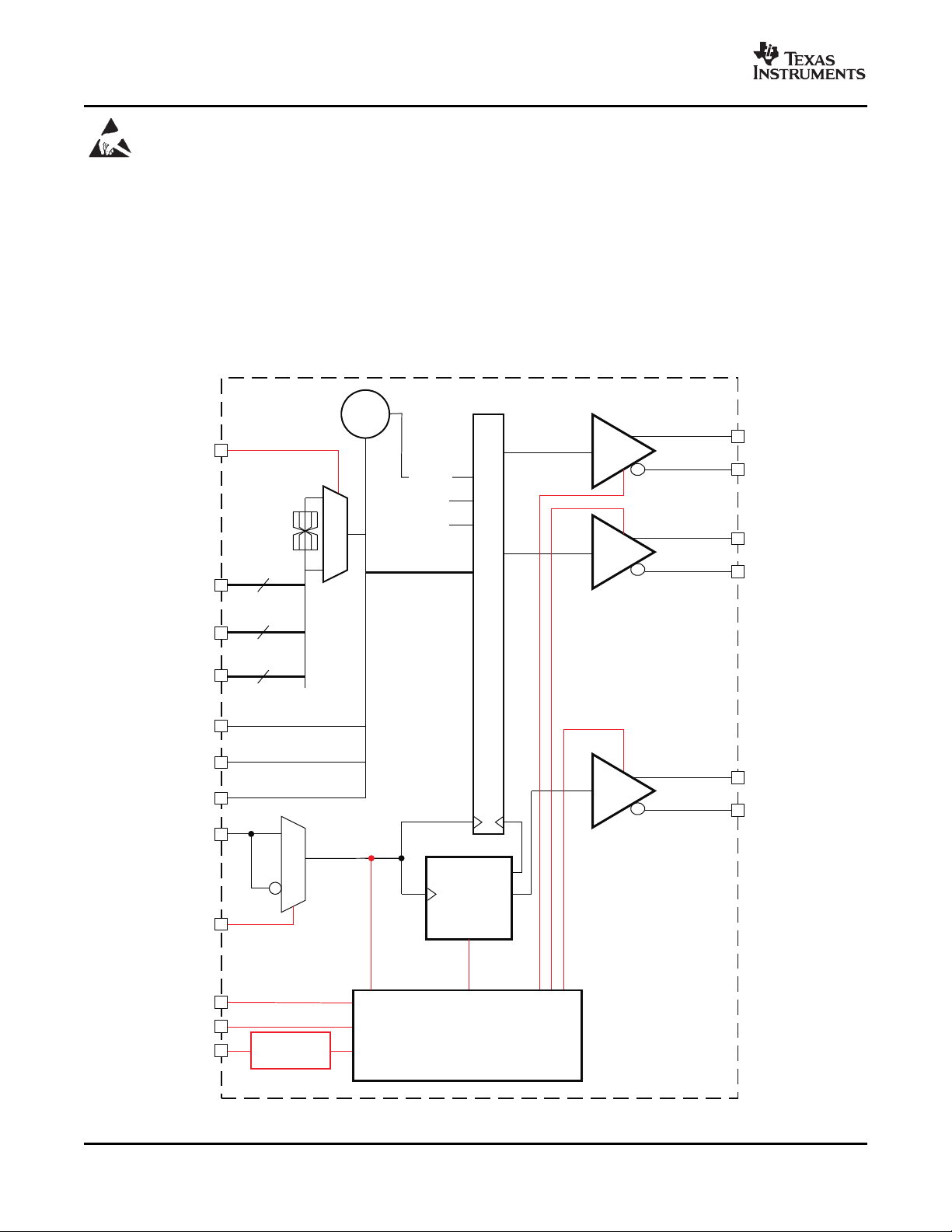
PROGRAMMABLE 27-BIT DISPLAY SERIAL-INTERFACE TRANSMITTER
SN65LVDS303
SLLS743A – JULY 2006 – REVISED JANUARY 2007
FEATURES
• FlatLink™3G Serial-Interface Technology
• Compatible With FlatLink3G Receivers Such
as SN65LVDS304
• Input Supports 24-bit RGB Video Mode
Interface
• 24-Bit RGB Data, 3 Control Bits, 1 Parity Bit
and 2 Reserved Bits Transmitted over 1 or 2
Differential Lines
• SubLVDS Differential Voltage Levels
• Effective Data Throughput up to 810 Mbps
• Three Operating Modes to Conserve Power
– Active-Mode QVGA 17.4 mW (typ)
– Active-Mode VGA 28.8 mW (typ)
– Shutdown Mode ≈ 0.5 µ A (typ)
– Standby Mode ≈ 0.5 µ A (typ)
• Bus Swap for Increased PCB Layout
Flexibility
• 1.8-V Supply Voltage
• ESD Rating > 2 kV (HBM)
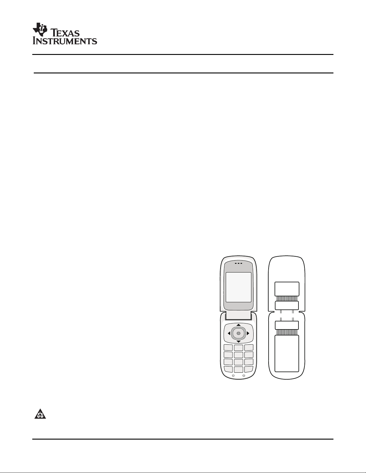
• Typical Application: Host-Controller to
Display-Module Interface
• Pixel Clock Range of 4 MHz–30 MHz
• Failsafe on All CMOS Inputs
• Packaging: 80-Terminal, 5-mm × 5-mm µ BGA
FPC cabling typically interconnects the
SN65LVDS303 with the display. Compared to
parallel signaling, the SN65LVDS303 outputs
significantly reduce the EMI of the interconnect by
over 20 dB.
The SN65LVDS303 supports three power modes
(shutdown, standby and active) to conserve power.
When transmitting, the PLL locks to the incoming
pixel clock, PCLK, and generates an internal
high-speed clock at the line rate of the data lines.
The parallel data are latched on the rising or falling
edge of PCLK, as selected by the external control
signal CPOL. The serialized data is presented on the
serial outputs D0 and D1, together with a recreated
PCLK that is generated from the internal high-speed
clock and output on CLK. If PCLK stops, the device
enters a standby mode to conserve power.
The parallel (CMOS) input bus offers a bus-swap
feature. The SWAP terminal configures the input
order of the pixel data to be either R[7:0], G[7:0],
B[7:0], VS, HS, DE or B[0:7]. G[0:7], R[0:7], VS, HS,
DE. This gives a PCB designer the flexibility to better
match the bus to the host controller pinout or to put
the transmitter device on the top side or the bottom
side of the PCB.
®
DESCRIPTION
The SN65LVDS303 serializer device converts 27
parallel data inputs to one or two sub-low-voltage
differential signaling (SubLVDS) serial outputs. It
loads a shift register with 24 pixel bits and 3 control
bits from the parallel CMOS input interface. In
addition to the 27 data bits, the device adds a parity
bit and two reserved bits into a 30-bit data word.
Each word is latched into the device by the pixel
clock (PCLK). The parity bit (odd parity) allows a
receiver to detect single bit errors. The serial shift
register is uploaded at 30 or 15 times the pixel-clock
data rate, depending on the number of serial links
used. A copy of the pixel clock is output on a
separate differential output.
FlatLink is a trademark of Texas Instruments.
µ BGA is a registered trademark of Tessera, Inc..
All other trademarks are the property of their respective owners.
PRODUCTION DATA information is current as of publication date.
Products conform to specifications per the terms of the Texas
Instruments standard warranty. Production processing does not
necessarily include testing of all parameters.
Please be aware that an important notice concerning availability, standard warranty, and use in critical applications of Texas
Instruments semiconductor products and disclaimers thereto appears at the end of this data sheet.
Copyright © 2006–2007, Texas Instruments Incorporated
www.ti.com
[0..26]
0
1
TXEN
PCLK
VS
HS
B[0:7]
G[0:7]
R[0:7]
DE
LS
8
8
8
D0+
D0–
SubLVDS
SubLVDS
SubLVDS
CLK+
CLK–
D1+
D1–
GND
CPOL
SWAP
1
0
iPCLK
Bit28=0
Bit27=0
Bit29
Glitch
Supression
Control/StandbyMonitor
Parity
Calc
2 15-or1 30-BitParallel-to-SerialConversion´ ´
´ ´15or 30
´1
PLL
Multiplier
SN65LVDS303
SLLS743A – JULY 2006 – REVISED JANUARY 2007
These devices have limited built-in ESD protection. The leads should be shorted together or the device placed in conductive foam
during storage or handling to prevent electrostatic damage to the MOS gates.
DESCRIPTION (CONTINUED)
The link select line, LS, controls whether one or two serial links are used. The TXEN input may be used to put
the SN65LVDS303 in a shutdown mode. The SN65LVDS303 enters an active standby mode if the input clock,
PCLK, stops. This minimizes power consumption without the need for controlling an external terminal. The
SN65LVDS303 is characterized for operation over ambient air temperatures of –40 ° C to 85 ° C. All CMOS inputs
offer failsafe to protect the input from damage during power up and to avoid current flow into the device inputs
during power up. An input voltage of up to 2.165 V can be applied to all CMOS inputs while V
and 1.65 V.
Functional Block Diagram
is between 0 V
DD
2
Submit Documentation Feedback
www.ti.com
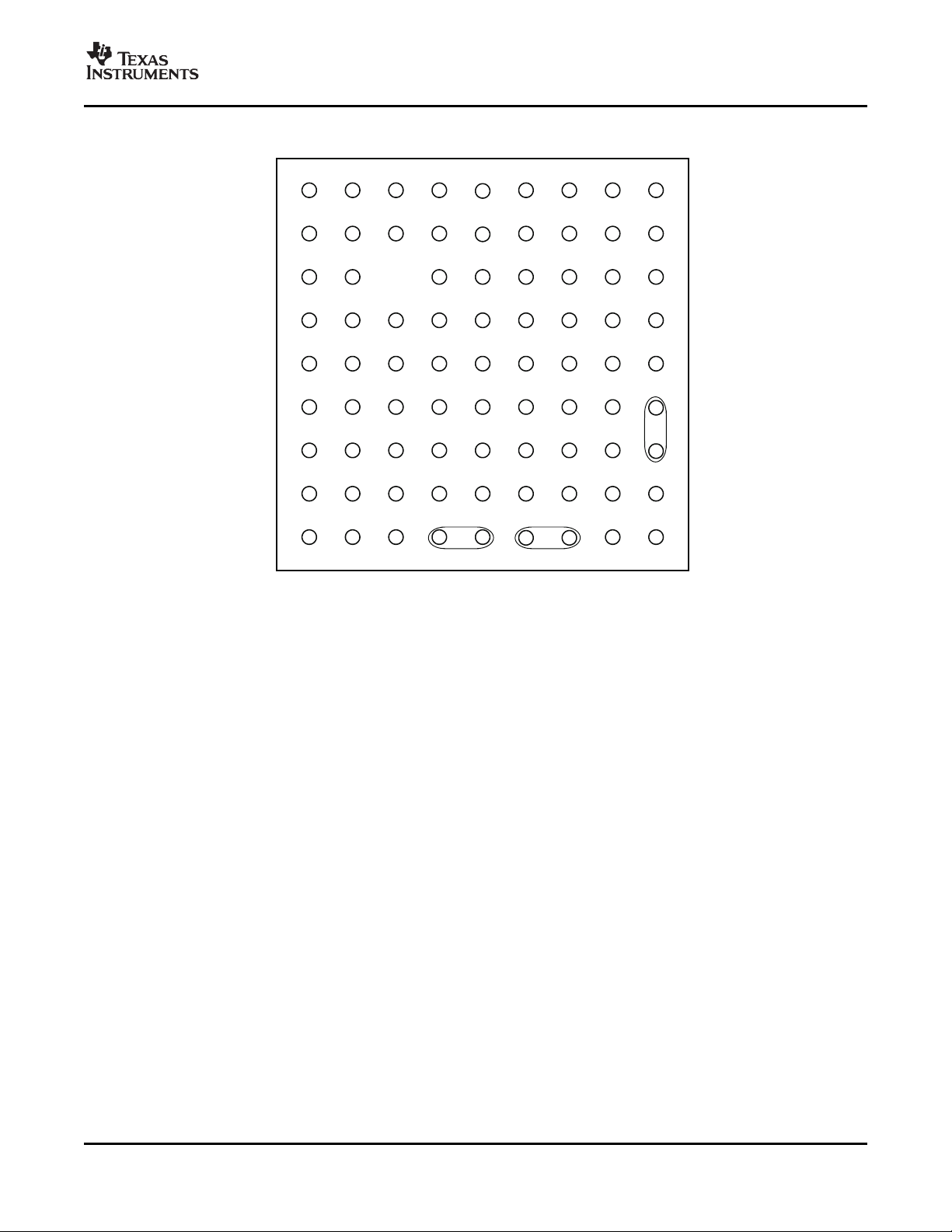
PINOUT – TOP VIEW
9
8764 5321
A
D
C
B
G
F
E
H
J
D0–
G0
/G7
B7/R0
NC
NC
D1+
D1-
D0+ CLK+
CLK–
R7/B0
V
DDLVDS
GND
LVDS
V
DDPLLD
GND
PLLD
GND
PLLA
VDD
B0/R7
GND
LVDS
GND
GND
VDD
DE
GND
GND
GND
HS VS
GND
GND
GND
GNDPCLK
TXEN
VDD
V
DDPLLA
GND
B5
/R2 VDD
B1
/R6
VDD
GND
B4
/R3
VDDB2/R5
B3/R4
GND
GND
GND GND
GND
GND
GND
GND
GND
GND
GND
B6
/R1
SWAP
GND
LS
CPOL
GND
VDD
V
DDLVDS
R1/B6
G6/G1
G5/G2G3/G4
G2/G5
G1/G6 R3/B4
R6/B1
R5/B2
R2/B5 R4/B3
G7/G0
R0/B7G4/G3
GND
LVDS
RGBInputpinassignmentbasedonSWAP pinsetting:
SWAP=0/SWAP=1
SN65LVDS303
SLLS743A – JULY 2006 – REVISED JANUARY 2007
Submit Documentation Feedback
3
www.ti.com
9
8764 5321
A
D
C
B
G
F
E
H
J
G0
B7
R7
B0
DE
HS VS
PCLK
B5
B1B4B2
B3
B6
R1
G6
G5G3
G2
G1 R3R6R5
R2 R4
G7
R0G4
SN65LVDS303
TopView
SWAP
SWAP=0
9
8764 5321
A
D
C
B
G
F
E
H
J
G7
R0
B0
R7
DE
HS VS
PCLK
R2
R6R3R5
R4
R1
B6
G1
G2G4
G5
G6 B4B1B2
B5 B3
G0
B7G3
SN65LVDS303
TopView
SWAP
SWAP=1
1.8V
SN65LVDS303
SLLS743A – JULY 2006 – REVISED JANUARY 2007
PINOUT – TOP VIEW (continued)
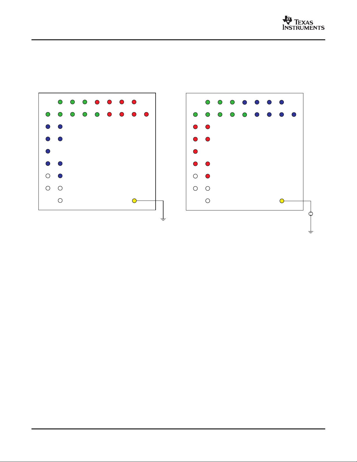
SWAP TERMINAL FUNCTIONALITY
The SWAP terminal allows the PCB designer to reverse the RGB bus, thus minimize potential signal crossovers
due to signal routing. Figure 1 and Figure 2 show the RGB signal terminal assignment based on the SWAP
terminal setting.
4
Figure 1. SWAP TERMINAL = 0 Figure 2. SWAP Terminal = 1
Submit Documentation Feedback
www.ti.com
SLLS743A – JULY 2006 – REVISED JANUARY 2007
Table 1. NUMERIC TERMINAL LIST
. . TERMINAL SWAP SIGNAL TERMINAL SWAP SIGNAL TERMINAL SWAP SIGNAL
A1 — GND 0 B6 0 B1
A2
A3
A4
A5
A6
A7 D1
A8 D2
0 G2 1 R1 1 R6
1 G5 0 B7 0 B2
0 G4 1 R0 1 R5
1 G3 C3 UNPOPULATED F3 — VDD
0 G6 C4 — VDD F4 — GND
1 G1 C5 — GND F5 — GND
0 R0 C6 — VDD F6 — GND
1 B7 C7 — VDD F7 — GND
0 R2 C8 — GND F8 — V
1 B5 C9 — LS F9 — D1+
0 R4 0 B4 G1 — PCLK
1 B3 1 R3 0 B0
0 R6 0 B5 1 R7
1 B1 1 R2 G3 — V
A9 — GND D3 — VDD G4 — GND
B1
B2
B3
B4 E1
B5
B6
B7
B8
B9
0 G0 D4 — GND G5 — GND
1 G7 D5 — GND G6 — GND
0 G1 D6 — GND G7 — GND
1 G6 D7 — GND G8 — GND
0 G3 D8 — GND G9 — D1–
1 G4 D9 — NC H1 — HS
0 G5 0 B3 H2 — VS
1 G2 1 R4 H3 — GND
0 G7 E2 — GND H4 — GND
1 G0 E3 — VDD H5 — V
0 R1 E4 — GND H6 — GND
1 B6 E5 — GND H7 — V
0 R3 E6 — GND H8 — V
1 B4 E7 — GND H9 — CPOL
0 R5 E8 — GND
1 B2 E9 — NC J2 — DE
0 R7 J3 — TXEN
1 B0 J4 — D0–
C1 F1
C2 F2
PLLD
G2
J1 — GND
J5 — D0+
J6 — CLK–
J7 — CLK+
J8 — SWAP
J9 — GND
SN65LVDS303
DDPLLD
DD
LVDS
LVDS
DDLVDS
PLLA
DDPLLA
DDLVDS
LVDS
Submit Documentation Feedback
5
www.ti.com
SN65LVDS303
SLLS743A – JULY 2006 – REVISED JANUARY 2007
Table 2. TERMINAL FUNCTIONS
NAME I/O DESCRIPTION
D0+, D0– SubLVDS data link (active during normal operation)
D1+, D1– SubLVDS out
CLK+, CLK– SubLVDS output clock; clock polarity is fixed.
R0–R7 Red pixel data (8); terminal assignment depends on SWAP terminal setting.
G0–G7 Green pixel data (8); terminal assignment depends on SWAP terminal setting.
B0–B7 Blue pixel data (8); terminal assignment depends on SWAP terminal setting.
HS Horizontal sync
VS Vertical sync
DE Data enable
PCLK Input pixel clock; rising or falling clock polarity is selected by control input CPOL.
LS Link select (determines active SubLVDS data links and PLL range); see Table 3 .
CMOS in
TXEN
CPOL CMOS in
SWAP CMOS in
V
DD
GND Supply ground
V
DDLVDS
GND
LVDS
V
DDPLLA
GND
PLLA
V
DDPLLD
GND
PLLD
Power supply
(1)
(1) For a multilayer PCB, it is recommended to keep one common GND layer underneath the device and connect all ground terminals
directly to this plane.
SubLVDS data link (active during normal operation when LS = high; high impedance if
LS = low)
Disables the CMOS drivers and turns off the PLL, putting device in shutdown mode
1 – Transmitter enabled
0 – Transmitter disabled (shutdown)
Note: The TXEN input incorporates glitch-suppression logic to avoid device malfunction
on short input spikes. It is necessary to pull TXEN high for longer than 10 µ s to enable
the transmitter. It is necessary to pull the TXEN input low for longer than 10 µ s to
disable the transmitter. At power up, the transmitter is enabled immediately if TXEN = 1
and disabled if TXEN = 0
Input clock polarity selection
0 – rising edge clocking
1 – falling edge clocking
Bus swap. Swaps the bus terminals to allow device placement on top or bottom of PCB.
See pinout drawing for terminal assignments.
0 – data input from B0...R7
1 – data input from R7...B0
Supply voltage
SubLVDS I/O supply voltage
SubLVDS ground
PLL analog supply voltage
PLL analog GND
PLL digital supply voltage
PLL digital GND
6
Submit Documentation Feedback
www.ti.com
D0+/– CHANNEL
CLK+
B7
B6
R7
R6
R5
R4
R3
R2 R1
R0
G7 G6 G5 G4G3G2 G1 G0
B5
B4
B3
B2 B1
B0
VS HS DE
0 0
CP R7
R6
CP
00
CLK–
R7
R6
R5
R4
R3
R2 R1
R0
G7 G6 G5 G4 VS0CP
0
B7
B6
G3
G2 G1 G0
B5
B4
B3
B2 B1
B0
HS DE
0
CP R7
R6
G3
G2
CLK+
CLK–
D0+/– Channel
D1+/– Channel
SN65LVDS303
SLLS743A – JULY 2006 – REVISED JANUARY 2007
FUNCTIONAL DESCRIPTION
Serialization Modes
The SN65LVDS303 transmitter has two modes of operation controlled by link-select terminal LS. Table 3 shows
the serializer modes of operation.
Table 3. Logic Table: Link Select Operating Modes
LS Mode of Operation Data Links Status
0 1-channel mode, 1ChM (30-bit serialization rate) D0 active; D1 high-impedance
1 2-channel mode, 2ChM (15-bit serialization rate) D0, D1 active
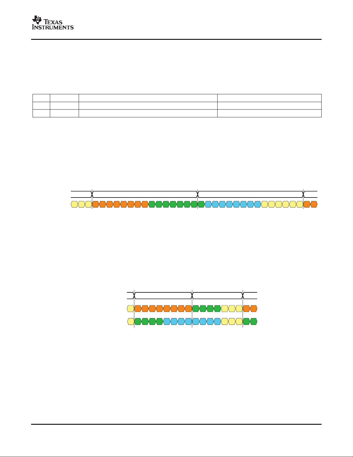
1-Channel Mode
While LS is held low, the SN65LVDS303 transmits payload data over a single SubLVDS data pair, D0. The PLL
locks to PCLK and internally multiplies the clock by a factor of 30. The internal high-speed clock is used to
serialize (shift out) the data payload on D0. Two reserved bits and the parity bit are added to the data frame.
Figure 3 illustrates the timing and the mapping of the data payload into the 30-bit frame. The internal high-speed
clock is divided by a factor of 30 to recreate the pixel clock, and presented on the SubLVDS CLK output. While
in this mode, the PLL can lock to a clock that is in the range of 4 MHz through 15 MHz. This mode is intended
for smaller video display formats (e.g. QVGA to HVGA) that do not require the full bandwidth capabilities of the
SN65LVDS303.
Figure 3. Data and Clock Output in 1-Channel Mode (LS = Low).
2-Channel Mode
While LS is held high, the SN65LVDS303 transmits payload data over two SubLVDS data pairs, D0 and D1. The
PLL locks to PCLK and internally multiplies it by a factor of 15. The internal high-speed clock is used to serialize
the data payload on D0 and D1. Two reserved bits and the parity bit are added to the data frame. Figure 4
illustrates the timing and the mapping of the data payload into the 30-bit frame and how the frame becomes split
into the two output channels. The internal high-speed clock is divided by 15 to recreate the pixel clock and
presented on SubLVDS CLK. The PLL can lock to a clock that is in the range of 8 MHz through 30 MHz in this
mode. Typical applications for using the 2-channel mode are HVGA and VGA displays.
Figure 4. Data and Clock Output in 2-Channel Mode (LS = High).
Power-Down Modes
The SN65LVDS303 transmitter has two power-down modes to facilitate efficient power management.
Shutdown Mode
The SN65LVDS303 enters shutdown mode when the TXEN terminal is asserted low. This turns off all
transmitter circuitry, including the CMOS input, PLL, serializer, and SubLVDS transmitter output stage. All
outputs are high-impedance. Current consumption in shutdown mode is nearly zero.
Submit Documentation Feedback
7

www.ti.com
SN65LVDS303
SLLS743A – JULY 2006 – REVISED JANUARY 2007
Standby Mode
The SN65LVDS303 enters the standby mode if TXEN is high and the PCLK input signal frequency is less than
500 kHz. All circuitry except the PCLK input monitor is shut down, and all outputs enter the high-impedance
state. The current consumption instandby mode is very low. When the PCLK input signal is completely stopped,
the IDDcurrent consumption is less than 10 µ A. The PCLK input must not be left floating.
NOTE:
A floating (left open) CMOS input allows leakage currents to flow from V
To prevent large leakage current, a CMOS gate must be kept at a valid logic level,
either V
or VIL. This can be achieved by applying an external voltage of V
IH
all SN65LVDS303 inputs.
Active Modes
When TXEN is high and the PCLK input clock signal is faster than 3 MHz, the SN65LVDS303 enters the active
mode. Current consumption in the active mode depends on operating frequency and the number of data
transitions in the data payload.
Acquire Mode (PLL Approaches Lock)
The PLL is enabled and attempts to lock to the input clock. All outputs remain in the high-impedance state.
When the PLL monitor detects stable PLL operation, the device switches from the acquire mode to the transmit
mode. For proper device operation, the pixel clock frequency must fall within the valid f
under recommended operating conditions. If the pixel clock frequency is higher than 3 MHz but lower than
f
(min), the SN65LVDS303 PLL is enabled. Under such conditions, it is possible for the PLL to lock
PCLK
temporarily to the pixel clock, causing the PLL monitor to release the device into transmit mode. If this happens,
the PLL may or may not be properly locked to the pixel clock input, potentially causing data errors, frequency
oscillation, and PLL deadlock (loss of VCO oscillation).
to GND.
DD
or V
IH
to
IL
range specified
PCLK
Transmit Mode
After the PLL achieves lock, the device enters the normal transmit mode. The CLK terminal outputs a copy of
PCLK. Based on the selected mode of operation, the D0 and D1 outputs carry the serialized data. In 1-channel
mode, the D1 outputs remain in the high-impedance state.
Parity Bit Generation
The SN65LVDS303 transmitter calculates the parity of the transmit data word and sets the parity bit accordingly.
The parity bit covers the 27-bit data payload consisting of 24 bits of pixel data plus VS, HS and DE. The two
reserved bits are not included in the parity generation. Odd-parity bit signaling is used. The transmitter sets the
parity bit if the sum of the 27 data bits results in an even number of ones. The parity bit is cleared otherwise.
This allows the receiver to verify parity and detect single bit errors.
8
Submit Documentation Feedback
www.ti.com
Standby
Mode
Transmit
Mode
Acquire
Mode
TXENHigh>10 sm
PowerUp
TXEN=0
PowerUp
TXEN=1
CLK Active
PLL AchievedLock
Shutdown
Mode
TXENLow
>10 sm
TXENLow
>10 sm
TXENLow
>10 sm
PCLK
StopsorLost
PCLK
StopsorLost
PCLK
Active
PowerUp
TXEN=1
CLKInactive
SLLS743A – JULY 2006 – REVISED JANUARY 2007
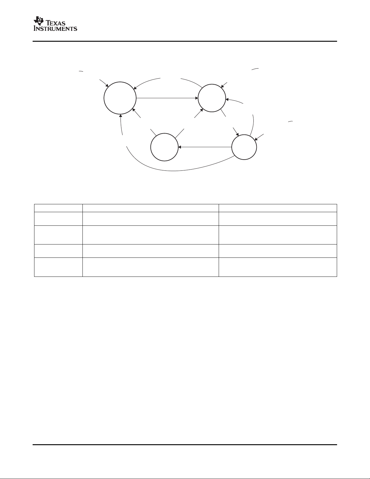
Status Detect and Operating Modes Flow diagram
The SN65LVDS303 switches between the power saving and active modes in the following way:
Figure 5. Status Detect and Operating Modes Flow Diagram
SN65LVDS303
Table 4. Status Detect and Operating Modes Descriptions
Mode Characteristics Conditions
Shutdown mode Least amount of power consumption
(1)
(most circuitry turned TXEN is low.
off); all outputs are high-impedance.
Standby mode Low power consumption (only clock activity circuit active; PLL TXEN is high; PCLK input signal is missing or
is disabled to conserve power); all outputs are inactive.
high-impedance.
Acquire mode PLL tries to achieve lock; all outputs are high-impedance. TXEN is high; PCLK input monitor detected input
activity.
Transmit mode Data transfer (normal operation); transmitter serializes data TXEN is high and PLL is locked to incoming clock.
and transmits data on serial output; unused outputs remain
high-impedance.
(1) In shutdown mode, all SN65LVDS303 internal switching circuits (e.g., PLL, serializer, etc.) are turned off to minimize power
consumption. The input stage of any input terminal remains active.
(2) Leaving inputs unconnected can cause random noise to toggle the input stage and potentially harm the device. All inputs must be tied to
a valid logic level VILor VIHduring shutdown or standby mode.
(1) (2)
(2)
Submit Documentation Feedback
9

www.ti.com
SN65LVDS303
SLLS743A – JULY 2006 – REVISED JANUARY 2007
Table 5. Operating Mode Transitions
MODE TRANSITION USE CASE TRANSITION SPECIFICS
Shutdown → standby Drive TXEN high to enable 1. TXEN high > 10 µ s
Standby → acquire Transmitter activity detected 1. PCLK input monitor detects clock input activity.
Acquire → transmit Link is ready to transfer data 1. PLL is active and approaches lock.
Transmit → standby Request transmitter to enter 1. PCLK Input monitor detects missing PCLK.
Transmit/standby → Turn off transmitter 1. TXEN pulled low for longer than 10 µ s
shutdown
transmitter
standby mode by stopping
PCLK
2. Transmitter enters standby mode.
a. All outputs are high-impedance.
b. Transmitter turns on clock input monitor.
2. Outputs remain high-impedance.
3. PLL circuit is enabled.
2. PLL achieved lock within 2 ms.
3. Parallel data input latches into shift register.
4. CLK output turns on.
5. Selected data outputs turn on and send out first serial data bit.
2. Transmitter indicates standby, putting all outputs into high-impedance.
3. PLL shuts down.
4. PCLK activity input monitor remains active.
2. Transmitter indicates standby, putting output CLK+ and CLK– into
high-impedance state.
3. Transmitter puts all other outputs into high-impedance state.
4. Most IC circuitry is shut down for least power consumption.
ORDERING INFORMATION
PART NUMBER Package SHIPPING METHOD
SN65LVDS303ZQER ZQE Reel
ABSOLUTE MAXIMUM RATINGS
over operating free-air temperature range (unless otherwise noted)
Supply voltage range, V
Voltage range at any input When V
or output terminal
Electrostatic discharge Charged-device model
Continuous power dissipation See Dissipation Ratings table
(1) Stresses beyond those listed under absolute maximum ratings may cause permanent damage to the device. These are stress ratings
only and functional operation of the device at these or any other conditions beyond those indicated under recommended operating
conditions is not implied. Exposure to absolute maximum-rated conditions for extended periods may affect device reliability.
(2) All voltage values are with respect to the GND terminals.
(3) In accordance with JEDEC Standard 22, Test Method A114-A.
(4) In accordance with JEDEC Standard 22, Test Method C101.
(5) In accordance with JEDEC Standard 22, Test Method A115-A
DD
(2)
, V
When V
Human-body model
Machine model
, V
DDPLLA
DDx
DDx
(1)
VALUE UNIT
, V
DDPLLD
DDLVDS
–0.3 to 2.175 V
> 0 V –0.5 to 2.175 V
≤ 0 V –0.5 to V
(3)
(all terminals) ± 3 kV
(4)
(all terminals) ± 500
(5)
(all terminals) ± 200
+ 2.175 V
DD
V
10
Submit Documentation Feedback

www.ti.com
SLLS743A – JULY 2006 – REVISED JANUARY 2007
DISSIPATION RATINGS
PACKAGE TA< 25 ° C
ZQE Low-K
(1) This is the inverse of the junction-to-ambient thermal resistance when board-mounted and with no air flow.
(2) In accordance with the low-K thermal metric definitions of EIA/JESD51-2.
CIRCUIT DERATING FACTOR
BOARD MODEL ABOVE TA= 25 ° C POWER RATING
(2)
592 mW 7.407 mW/ ° C 148 mW
THERMAL CHARACTERISTICS
PARAMETER TEST CONDITIONS VALUE UNIT
Typical V
P
Device power dissipation
D
Maximum V
= 1.8 V, TA= 25 ° C, 2-channel mode mW
DDx
= 1.95 V, TA= –40 ° C mW
DDx
PCLK at 4 MHz 14.4
PCLK at 30 MHz 38.2
PCLK at 4 MHz 22.3
PCLK = 30 MHz 50.2
SN65LVDS303
(1)
TA= 85 ° C
RECOMMENDED OPERATING CONDITIONS
(1)
MIN NOM MAX UNIT
V
DD
V
DDPLLA
V
DDPLLD
V
DDLVDS
V
DDn(PP)
Supply voltages 1.65 1.8 1.95 V
Supply voltage noise
magnitude 50 MHz (all 100 mV
supplies)
Test setup see Figure 11
f(noise) = 1Hz to 2 GHz
1-channel transmit mode, see Figure 3 4 15
f
PCLK
tH× f
T
t
jit(per)PCLK
t
jit(TJ)PCLK
t
jit(CC)PCLK
Pixel clock frequency MHz
PCLK
A
PCLK input duty cycle 0.33 0.67
Operating free-air
temperature
PCLK RMS period jitter
PCLK total jitter 0.05/f
PCLK peak s
cycle-to-cycle jitter
(4)
2-channel transmit mode, see Figure 4 8 30
Frequency threshold, standby mode to active
(2)
mode
, see Figure 15
0.5 3
–40 85 ° C
(3)
Measured on PCLK input
5 ps-rms
PCLK
0.02/f
PCLK
PCLK, R[0:7], G[0:7], B[0:7], VS, HS, DE, PCLK, LS, CPOL, TXEN, SWAP
V
IH
V
IL
t
DS
t
DH
High-level input voltage 0.7 V
DD
Low-level input voltage 0.3 V
Data set up time prior to
PCLK transition
Data hold time after PCLK
transition
f (PCLK) = 30 MHz; see Figure 7
2 ns
2 ns
V
DD
DD
(1) Unused single-ended inputs must be held high or low to prevent them from floating.
(2) PCLK input frequencies lower than 500 kHz force the SN65LVDS303 into standby mode. Input frequencies between 500 kHz and 3
MHz may or may not activate the SN65LVDS303. Input frequencies beyond 3 MHz activate the SN65LVDS303.
(3) Period jitter is the deviation in cycle time of a signal with respect to the ideal period over a random sample of 100,000 cycles.
(4) Cycle-to-cycle jitter is the variation in cycle time of a signal between adjacent cycles; over a random sample of 1,000 adjacent cycle
pairs.
s
V
V
Submit Documentation Feedback
11

www.ti.com
SN65LVDS303
SLLS743A – JULY 2006 – REVISED JANUARY 2007
DEVICE ELECTRICAL CHARACTERISTICS
over recommended operating conditions (unless otherwise noted)
PARAMETER TEST CONDITIONS MIN TYP
V
= V
DD
R
L(PCLK)
TXEN at VDD,
1ChM
alternating 1010 serial bit pattern
V
= V
DD
R
L(PCLK)
TXEN at VDD,
typical power test pattern (see Table 7 )
V
= V
DD
R
L(PCLK)
I
DD
2ChM
TXEN at VDD,
alternating 1010 serial bit pattern
V
= V
DD
R
L(PCLK)
TXEN at VDD,
typical power test pattern (see Table 8 )
Standby mode V
Shutdown mode 0.55 10 µ A
(1) All typical values are at 25 ° C and with 1.8 V supply unless otherwise noted.
= V
DDPLLA
= R
= 100 Ω , VIH= VDD, VIL= 0 V,
L(Dx)
= V
DDPLLA
= R
= 100 Ω , VIH= VDD, VIL= 0 V,
L(Dx)
= V
DDPLLA
= R
= 100 Ω , VIH= VDD, VIL= 0 V,
L(Dx)
= V
DDPLLA
= R
= 100 Ω , VIH= VDD, VIL= 0 V,
L(Dx)
= V
DDPLLD
= V
DDPLLD
= V
DDPLLD
= V
DDPLLD
DDLVDS
DDLVDS
DDLVDS
DDLVDS
, f
, f
, f
, f
= 4 MHz 9 11.4
PCLK
f
= 6 MHz 10.6 12.6
PCLK
f
= 15 MHz 16 18.8
PCLK
= 4 MHz 8
PCLK
f
= 6 MHz 8.9
PCLK
f
= 15 MHz 14
PCLK
= 8 MHz 13.7 15.9
PCLK
f
= 22 MHz 18.4 22
PCLK
f
= 30 MHz 21.4 25.8
PCLK
= 8 MHz 11.5
PCLK
f
= 22 MHz 16
PCLK
f
= 30 MHz 19.1
PCLK
= V
DD
= V
DDLVDS
R
= 100 Ω , VIH=
L(Dx)
VDD, VIL= 0 V, all inputs
= V
DDPLLA
, R
DDPLLD
=
L(PCLK)
held static high or static
low
(1)
MAX UNIT
0.61 10 µ A
mA
mA
mA
mA
OUTPUT ELECTRICAL CHARACTERISTICS
over operating free-air temperature range (unless otherwise noted)
PARAMETER TEST CONDITIONS MIN TYP
SubLVDS Output (D0+, D0–, D1+, D1–, CLK+, and CLK–)
V
OC(SS)M
V
OCM(SS)
V
OCM(PP)
|V
OD
∆ |V
Z
OD(CLK)
I
OSD
I
OS
I
OZ
(1) All typical values are at 25 ° C and with 1.8-V supply, unless otherwise noted.
(2) All SN65LVDS303 outputs tolerate shorts to GND or V
Steady-state common-mode output voltage Output load see Figure 9 0.8 0.9 1.0 V
Change in steady-state common-mode output voltage –10 10 mV
Peak-to-peak common mode output voltage 75 mV
Differential output voltage magnitude
| 100 150 200 mV
|V
– V
Dx+
| Change in differential output voltage between logic states –10 10 mV
OD
|, |V
Dx–
Differential small-signal output impedance TXEN at V
Differential short-circuit output current V
Short circuit output current
– V
CLK+
CLK–
|
DD
= 0 V, f
(2)
OD
VO= 0 V or V
= 28 MHz 10
PCLK
DD
High-impedance state output current VO= 0 V or VDD(max), –3 3
TXEN at GND
without device damage.
DD
INPUT ELECTRICAL CHARACTERISTICS
over operating free-air temperature range (unless otherwise noted)
PARAMETER TEST CONDITIONS MIN TYP
PCLK, R[0:7], G[0:7], B[0:7], VS, HS, DE, PCLK, LS, CPOL, TXEN, SWAP
I
High-level input current VIN= 0.7 × V
IH
I
Low-level input current VIN= 0.3 × V
IL
C
Input capacitance 1.5 pF
IN
DD
DD
(1) All typical values are at 25 ° C and with 1.8-V supply, unless otherwise noted.
–200 200
–200 200
(1)
MAX UNIT
210 Ω
5
(1)
MAX UNIT
mA
µ A
nA
12
Submit Documentation Feedback

www.ti.com
SWITCHING CHARACTERISTICS
f − PLL Frequency − MHz
4
5
6
7
8
9
10
11
12
0 100 200 300 400 500 600
PLL BW (% of PCLK Frequency) − %
G001
8.1 %
7.6 %
9 %
8.5 %
RX PLL BW
TX PLL BW
6.0
6.5
7.0
7.5
8.0
8.5
9.0
0 5 10 15 20 25 30 35 40
4 MHz:
8.5%
PLL Bandwidth − %
15
MHz:
7.6%
8 MHz:
8.5%
30 MHz:
7.6%
Spec
Limit
1 ChM
Spec
Limit
2 ChM
f − PCLK Frequency − MHz
G002
over recommended operating conditions (unless otherwise noted)
PARAMETER TEST CONDITIONS MIN TYP
t
r
t
f
f
BW
t
pd(L)
tH× f
t
GS
t
pwrup
t
pwrdn
t
wakup
t
sleep
20%-to-80% differential
output signal rise time
20%-to-80% differential
output signal fall time
See Figure 8 and Figure 9 250 500
See Figure 8 and Figure 9 250 500
PLL bandwidth (3dB cutoff Tested from PCLK input to
frequency) CLK output, See Figure 6
Propagation delay time, 1-channel mode 0.8/f
input to serial output (data s
latency Figure 10 )
Output CLK duty cycle
CLK0
TXEN Glitch suppression VIH= VDD, VIL= GND, TXEN toggles between VILand VIH,
pulse duration
(3)
TXEN at VDD, VIH=V
VIL=GND, RL=100 Ω
see Figure 13 and Figure 14 .
Enable time from power Time from TXEN pulled high to CLK and Dx outputs
down ( ↑ TXEN) enabled and transmit valid data; see Figure 14
Disable time from active
mode ( ↓ TXEN)
Enable time from standby
( ↕ PCLK)
Disable time from active
mode (PCLK stopping)
TXEN is pulled low during transmit mode; time
measurement until output is disabled and PLL is 0.5 11 µ s
Shutdown; see Figure 14
TXEN at VDD; device in standby; time measurement from
PCLK starts switching to CLK and Dx outputs enabled and 0.23 2 ms
transmit valid data; see Figure 14
TXEN at VDD; device is transmitting; time measurement
from PCLK input signal stops until CLK + Dx outputs are 0.4 100 µ s
disabled and PLL is disabled; see Figure 14
SN65LVDS303
SLLS743A – JULY 2006 – REVISED JANUARY 2007
(1)
f
= 22 MHz 0.082 f
PCLK
(2)
f
= 30 MHz 0.078 f
PCLK
,
DD
2-channel mode 1/f
PCLK
PCLK
1/f
PCLK
1.21/f
PCLK
1-channel mode 0.45 0.50 0.55
2-channel mode 0.49 0.53 0.58
3.8 10 µ s
0.24 2 ms
MAX UNIT
ps
PCLK
MHz
PCLK
1.2/f
PCLK
1.5/f
PCLK
(1) All typical values are at 25 ° C and with 1.8-V supply unless otherwise noted.
(2) The Maximum Limit is based on statistical analysis of the device performance over process, voltage, and temp ranges. This parameter
is functionality tested only on Automatic Test Equipment (ATE).
(3) The TXEN input incorporates glitch-suppression circuitry to disregard short input pulses. tGSis the duration of either a high-to-low or
low-to-high transition that is suppressed.
Figure 6. SN65LVDS303 PLL Bandwidth (Also Showing the SN65LVDS304 PLL Bandwidth)
Submit Documentation Feedback
13

www.ti.com
ps330
f30
x
PCLK
-
×
ps330
f30
x
PCLK
+
×
PCLK
x – 0.1845
f30 ×
PCLK
f30
x 0.1845+
×
ps330
f15
x
PCLK
-
×
ps330
f15
x
PCLK
+
×
PCLK
x – 0.1845
f15 ×
PCLK
x+0.1845
f15 ×
R[7:0],G[7:0],B[7:0];
VS,HS,DE,LS, TXEN,
SWAP,CPOL
PCLK
(CPOL =Low)
t
DS
t
DH
t
R
V
IH
V
IL
V
IH
V
IL
0 V
20%
80%
150mV (nom)
−150mV (nom)
t
f
t
r
V
OD
SN65LVDS303
SLLS743A – JULY 2006 – REVISED JANUARY 2007
TIMING CHARACTERISTICS
PARAMETER TEST CONDITIONS MIN TYP MAX UNIT
1ChM: x = 0..29, f
at VDD, VIH= VDD, VIL= GND, RL= 100
Ω , test pattern as in Table 11
1ChM: x = 0..29,
f
= 4 MHz to 15 MHz
Output pulse position,
t
serial data to ↑ CLK; see ps
PPOSX
and Figure 12
PCLK
2ChM: x = 0..14, f
TXEN at VDD, VIH= VDD, VIL= GND, R
= 100 Ω , test pattern as in Table 12
2ChM: x = 0..14,
f
= 8 MHz to 30 MHz
PCLK
(1) This number also includes the high-frequency random and deterministic PLL clock jitter that is not traceable by the SN65LVDS304
receiver PLL; tPPosx represents the total timing uncertainty of the transmitter necessary to calculate the jitter budget when combined
with the SN65LVDS304 receiver.
(2) The pulse position min/max variation is given with a bit error rate target of 10
contribution to the total jitter by multiplying the random RMS jitter by the factor 14; measurements of the total jitter are taken with > 10
samples.
(3) The minimum and maximum limits are based on statistical analysis of the device performance over process, voltage, and temp ranges.
This parameter is functionality tested only on automatic test equipment (ATE).
(4) These minimum and maximum limits are simulated only.
PARAMETER MEASUREMENT INFORMATION
= 15 MHz; TXEN
PCLK
(3)
(4)
= 30 MHz(1) (2)
PCLK
(4)
L
(3)
–12
; the measurement estimates the random jitter
–12
Figure 7. Setup/Hold Time
Figure 8. Rise and Fall Time Definitions
14
Submit Documentation Feedback

www.ti.com
SN65LVDS303
CLK–,Dx–
CLK+,Dx+
975mV(Nom)
825mV(Nom)
R1=49.9 W
R2=49.9 W
C2=1pFC1=1pF
C3=1pF
V
OD
VDx+orVCLK+
VDx– orVCLK–
V
OCM
V
OCM
V (pp)
OCM
V (ss)
OCM
NOTES:
A.20-MHzoutputtestpatternonalldifferentialoutputs(CLK,D0,andD1):
thisisachievedby:
B.C1,C2,andC3includeinstrumentationandfixturecapacitance,tolerance±20%;C,R1,andR2tolerance±1%
C. ThemeasurementofV (pp)andV (ss)aretakenwithtestequipmentbandwidth>1GHz.
OCM OC
1.Deviceissetto2-channelmode.
2.f =20MHz
3.InputsR[7:3]=B[7:3]connectedtoV ,allotherdatainputssettoGND.
PCLK
DD
R6
(n)
R7
(n−1)
R7
R6
R7
D0+
CLK+
CLK−
CMOS
DataIn
PCLK
R6
CP CP
pixel
(n)
pixel
(n+1)
R7
(n)
R7
(n+1)
R6
(n+1)
R6
(n−1)
t
PROP
VDD/2
R6
(n−1)
R7
(n−1)
pixel
(n−2)
pixel
(n−1)
R6
(n)
R7
(n)
Note: Thegeneratorregulatesthe
noiseamplitudeatpointtothe
targetamplitudegivenunderthetable
RecommendedOperatingConditions
Noise
Generator
100mV
SN65LVDS303
V
DDPLLA
V
DDPLLD
V
DD
V
DDLVDS
GND
10 Fm
21
1
1
1.8-V
Supply
PARAMETER MEASUREMENT INFORMATION (continued)
Figure 9. Driver Output Voltage Test Circuit and Definitions
SN65LVDS303
SLLS743A – JULY 2006 – REVISED JANUARY 2007
Figure 10. t
Propagation Delay Input to Output (LS = 0; CPOL = 0)
pd(L)
Figure 11. Power Supply Noise Test Setup
Submit Documentation Feedback
15

www.ti.com
CLK+
Bit0
Bit1 Bit2
Bitx
Bit0
Bit1
CLK–
t
CLK+
CurrentCycle NextCycle
t
PPOS0
t
PPOS1
t
PPOS2
t
PPOSx
D[0:m]±
Note:
1-ChannelMode:x=0...29;m=0
2-ChannelMode:x=0...14;m=1
TXEN
PCLK
VCOInternalSignal
CLK
D0,D1
t
GS
VDD/2
PLL ApproachesLock
t
pwr up
SN65LVDS303
SLLS743A – JULY 2006 – REVISED JANUARY 2007
PARAMETER MEASUREMENT INFORMATION (continued)
Figure 12. t
SubLVDS Output Pulse Position Measurement
SK(0)
Figure 13. Transmitter Behavior While Approaching Sync
16
Submit Documentation Feedback

www.ti.com
CLK+
PCLK
t
wakeup
t
sleep
TransmitterDisabled
(OFF)
Transmitter AquiresLock,
OutputsStillDisabled
TransmitterEnabled,
OutputDataValid
Transmitter
Enabled,
OutputData
Valid
Transmitter
Disabled
(OFF)
PARAMETER MEASUREMENT INFORMATION (continued)
SN65LVDS303
SLLS743A – JULY 2006 – REVISED JANUARY 2007
Figure 14. Transmitter Enable Glitch Suppression Time
Figure 15. Standby Detection
Power Consumption Tests
Table 6 shows an example test pattern word.
Table 6. Example Test Pattern Word
Word R[7:4], R[3:0], G[7:4], G[3:0], B[7:4], B[3:0], 0, VS, HS, DE
1 0x7C3E1E7
7 C 3 E 1 E 7
R7 R6 R5 R4 R3 R2 R1 R0 G7 G6 G5 G4 G3 G2 G1 G0 B7 B6 B5 B4 B3 B2 B1 B0 0 VS HS DE
0 1 1 1 1 1 0 0 0 0 1 1 1 1 1 0 0 0 0 1 1 1 1 0 0 1 1 1
Typical IC Power-Consumption Test Pattern
The typical power-consumption test patterns consists of 16 30-bit transmit words in 1-channel mode, eight 30-bit
transmit words in 2-channel mode. The pattern repeats itself throughout the entire measurement. It is assumed
that every possible transmit code on RGB inputs has the same probability to occur during typical device
operation.
Submit Documentation Feedback
17

www.ti.com
SN65LVDS303
SLLS743A – JULY 2006 – REVISED JANUARY 2007
Table 7. Typical IC Power-Consumption Test Pattern,
Word Test Pattern:
1-Channel Mode
R[7:4], R[3:0], G[7:4], G[3:0], B[7:4], B[3:0], 0, VS, HS, DE
1 0x0000007
2 0xFFF0007
3 0x01FFF47
4 0xF0E07F7
5 0x7C3E1E7
6 0xE707C37
7 0xE1CE6C7
8 0xF1B9237
9 0x91BB347
10 0xD4CCC67
11 0xAD53377
12 0xACB2207
13 0xAAB2697
14 0x5556957
15 0xAAAAAB3
16 0xAAAAAA5
Table 8. Typical IC Power Consumption Test Pattern,
2-Channel Mode
Word Test Pattern:
R[7:4], R[3:0], G[7:4], G[3:0], B[7:4], B[3:0], 0, VS, HS, DE
1 0x0000001
2 0x03F03F1
3 0xBFFBFF1
4 0x1D71D71
5 0x4C74C71
6 0xC45C451
7 0xA3AA3A5
8 0x5555553
Maximum Power Consumption Test Pattern
The maximum (or worst-case) power consumption of the SN65LVDS303 is tested using the two different test
pattern shown in table. test patterns consists of sixteen 30-bit transmit words in 1-channel mode, eight 30-bit
transmit words in 2-channel mode. The pattern repeats itself throughout the entire measurement. It is assumed
that every possible transmit code on RGB inputs has the same probability to occur during typical device
operation.
Table 9. Worst-Case Power Consumption Test Pattern
Word Test Pattern:
R[7:4], R[3:0], G[7:4], G[3:0], B[7:4], B[3:0], 0, VS, HS, DE
1 0xAAAAAA5
2 0x5555555
18
Submit Documentation Feedback

www.ti.com
SN65LVDS303
SLLS743A – JULY 2006 – REVISED JANUARY 2007
Table 10. Worst-Case Power Consumption Test Pattern
Word Test Pattern:
Output Skew Pulse Position and Jitter Performance
The following test patterns are used to measure the output skew pulse position and the jitter performance of the
SN65LVDS303. The jitter test patterns stress the interconnect for worst-case ISI. Each pattern is self-repeating
for the duration of the test.
Table 11. Transmit Jitter Test Pattern, 1-Channel Mode
Word Test Pattern:
R[7:4], R[3:0], G[7:4], G[3:0], B[7:4], B[3:0], 0, VS, HS, DE
1 0x0000000
2 0xFFFFFF7
R[7:4], R[3:0], G[7:4], G[3:0], B[7:4], B[3:0], 0, VS, HS, DE
1 0x0000001
2 0x0000031
3 0x00000F1
4 0x00003F1
5 0x0000FF1
6 0x0003FF1
7 0x000FFF1
8 0x0F0F0F1
9 0x0C30C31
10 0x0842111
11 0x1C71C71
12 0x18C6311
13 0x1111111
14 0x3333331
15 0x2452413
16 0x22A2A25
17 0x5555553
18 0xDB6DB65
19 0xCCCCCC1
20 0xEEEEEE1
21 0xE739CE1
22 0xE38E381
23 0xF7BDEE1
24 0xF3CF3C1
25 0xF0F0F01
26 0xFFF0001
27 0xFFFC001
28 0xFFFF001
29 0xFFFFC01
30 0xFFFFF01
31 0xFFFFFC1
32 0xFFFFFF1
Submit Documentation Feedback
19

www.ti.com
SN65LVDS303
SLLS743A – JULY 2006 – REVISED JANUARY 2007
Table 12. Transmit Jitter Test Pattern, 2-Channel Mode
Word Test Pattern:
R[7:4], R[3:0], G[7:4], G[3:0], B[7:4], B[3:0], 0, VS, HS, DE
1 0x0000001
2 0x000FFF3
3 0x8008001
4 0x0030037
5 0xE00E001
6 0x00FF001
7 0x007E001
8 0x003C001
9 0x0018001
10 0x1C7E381
11 0x3333331
12 0x555AAA5
13 0x6DBDB61
14 0x7777771
15 0x555AAA3
16 0xAAAAAA5
17 0x5555553
18 0xAAA5555
19 0x8888881
20 0x9242491
21 0xAAA5571
22 0xCCCCCC1
23 0xE3E1C71
24 0xFFE7FF1
25 0xFFC3FF1
26 0xFF81FF1
27 0xFE00FF1
28 0x1FF1FF1
29 0xFFCFFC3
30 0x7FF7FF1
31 0xFFF0007
32 0xFFFFFF1
20
Submit Documentation Feedback

www.ti.com
T − Temperature − °C
−50 −30 −10 10 30 50 70 90
Standby Current
IDDQ − Supply Current − µA
1
0.1
G003
Power−Down Current
T − Temperature − °C
0
5
10
15
20
−50 −30 −10 10 30 50 70 90
2-Channel Mode, 22 MHz (VGA)
I
DD
− Supply Current − mA
G004
2-Channel Mode, 11 MHz (HVGA)
f − PCLK Frequency − MHz
5
10
15
20
25
30
0 5 10 15 20 25 30
2-Channel Mode
I
DD
− Supply Current − mA
G005
1-Channel Mode
f − PCLK Frequency − MHz
100
110
120
130
140
150
160
170
180
190
200
0 5 10 15 20 25 30
85°C
V
OD
− Differential Output Swing − mV
G006
–40°C
25°C
f − PCLK Frequency − MHz
5.0
5.5
6.0
6.5
7.0
7.5
8.0
8.5
9.0
9.5
10.0
0 5 10 15 20 25 30 35 40
PLL Bandwidth − %
G007
Spec Limit 2
ChM
30 MHz: 7.6%
Spec Limit 1
ChM
15 MHz: 7.6%
Spec Limit 2 ChM 8 MHz: 8.5%
2-ChM
Spec Limit
1 ChM
4 MHz: 8.5%
f − PCLK Frequency − MHz
0
100
200
300
400
500
0 5 10 15 20 25 30
CC Output Jitter − ps
G008
1-Channel Mode
2-Channel Mode
SN65LVDS303
SLLS743A – JULY 2006 – REVISED JANUARY 2007
TYPICAL CHARACTERISTICS
POWERDOWN, STANDBY SUPPLY CURRENT
vs TEMPERATURE SUPPLY CURRENT IDDvs TEMPERATURE
Figure 16. Figure 17.
SUPPLY CURRENT vs PCLK FREQUENCY DIFFERENTIAL OUTPUT SWING vs PCLK FREQUENCY
Figure 18. Figure 19.
PLL BANDWIDTH vs PCLK FREQUENCY
Figure 20. Figure 21.
Submit Documentation Feedback
CYCLE-TO-CYCLE OUTPUT JITTER
21

www.ti.com
T − Temperature − °C
0
50
100
150
200
−50 −25 0 25 50 75 100
2-Channel Mode,
f(PCLK) = 11 MHz
CC Output Jitter − ps
G009
1-Channel Mode,
f(PCLK) = 22 MHz
T − Temperature − °C
0
20
40
60
80
100
120
−50 −25 0 25 50 75 100
2-Channel Mode,
11 MHz (VGA)
t
PPOS
− Output Pulse Position − ps
G010
2-Channel Mode,
22 MHz (HVGA)
f − Frequency − MHz
−15
−10
−5
0
0 500 1000 1500 2000
Output Return Loss − dB
G011
D1
D0
CLK
f − Frequency − MHz
−20
−15
−10
−5
0
0 500 1000 1500 2000
Output Common-Mode Noise Rejection − dB
G012
D1
D0
CLK
f − Frequency − MHz
−100
−80
−60
−40
−20
0
0 500 1000 1500 2000
Isolation − dB
G013
D0 to D1
SN65LVDS303
SLLS743A – JULY 2006 – REVISED JANUARY 2007
TYPICAL CHARACTERISTICS (continued)
CYCLE-TO-CYCLE OUTPUT JITTER
vs TEMPERATURE OUTPUT PULSE POSITION vs TEMPERATURE
Figure 22. Figure 23.
OUTPUT RETURN LOSS OUTPUT COMMON MODE NOISE REJECTION
Figure 24. Figure 25.
22
CROSSTALK
Figure 26.
Submit Documentation Feedback

www.ti.com
22MHz
27
PCLK
D[7:0]
D[15:8]
D[23:16]
HS,VS,DE
R[7:0]
G[7:0]
B[7:0]
HS,VS,DE
R[7:0]
G[7:0]
B[7:0]
HS,VS,DE
PixelCLK
2 0.1 F´ m 2 0.1 F´ m
2 0.01 F´ m 2 0.01 F´ m
D0+ D0+
D0– D0–
CLK+ CLK+
CLK– CLK–
D1+ D1+
D1– D1–
GND GND
1.8V 1.8V
2.7V 2.7V
GND GND
22MHz
27
PCLK
3
SN65LVDS303 SN65LVDS304
FPC
22MHz
330Mbps
330Mbps
Application
Processor
(e.g.OMAP)
SPI
LS
LS
VDDx
VDDx
GND
GND
TXEN
RXEN
ENABLE
SPI
RESET
SerialPortInterface
(3-WireIF)
1.8V 1.8V
IfFPCwirecountiscritica,replacethis
connectionwithapull-upresistoratRXEN
LCDWithVGA
Resolution
VideoModeDisplay
Driver
SN65LVDS303
SLLS743A – JULY 2006 – REVISED JANUARY 2007
APPLICATION INFORMATION
Preventing Increased Leakage Currents in Control Inputs
A floating (left open) CMOS input allows leakage currents to flow from V
input unconnected or floating. Every input must be connected to a valid logic level, V
supplied to V
. This also minimizes the power consumption of standby and power-down modes.
DD
Power Supply Design Recommendation
For a multilayer PCB, it is recommended to keep one common GND layer underneath the device and connect all
ground terminals directly to this plane.
Decoupling Recommendation
The SN65LVDS303 was designed to operate reliably in a constricted environment with other digital switching
ICs. In cell phone designs, the SN65LVDS303 often shares a power supply with the application processor. The
SN65LVDS303 can operate with power supply noise as specified in Recommend Device Operating Conditions.
To minimize the power-supply noise floor, provide good decoupling near the SN65LVDS303 power terminals.
The use of four ceramic capacitors (2 × 0.01 µ F and 2 × 0.1 µ F) provides good performance. At the very least, it
is recommended to install one 0.1 µ F and one 0.01 µ F capacitor near the SN65LVDS303. To avoid large current
loops and trace inductance, the trace length between decoupling capacitor and IC power inputs terminals must
be minimized. Placing the capacitor underneath the SN65LVDS303 on the bottom of the PCB is often a good
choice.
to GND. Do not leave any CMOS
DD
or VIL, while power is
IH
VGA Application
Figure 27 shows a possible implementation of a VGA display. The SN65LVDS303 interfaces to the
SN65LVDS304, which is the corresponding receiver device to deserialize the data and drive the display driver.
The pixel clock rate of 22 MHz assumes ~10% blanking overhead and 60-Hz display refresh rate. The
application assumes 24-bit color resolution. It is also shown how the application processor provides a
power-down (reset) signal for both serializer and the display driver. The signal count over the FPC could be
further decreased by using the standby option on the SN65LVDS304 and pulling RXEN high with a 30-k Ω
resistor to V
.
DD
Figure 27. Typical VGA Display Application
Submit Documentation Feedback
23

www.ti.com
SN65LVDS303
SLLS743A – JULY 2006 – REVISED JANUARY 2007
APPLICATION INFORMATION (continued)
Typical Application Frequencies
The SN65LVDS303 supports pixel clock frequencies from 4 MHz to 30 MHz over one or two data pairs.
Table 13 provides a few typical display resolution examples and shows the number of data pairs necessary to
connect the LVDS303 with the display. The blanking overhead is assumed to be 20%. Often, blanking overhead
is smaller, resulting in a lower data rate. Futhermore, the examples in the table assume a display frame refresh
rate of 60-HZ or 90-Hz. The actual refresh rate may differ depending on the application-processor clock
implementation.
Table 13. Typical Application Data Rates and Serial Pair Usage
Display Screen Visible Pixel Blanking Display Pixel Clock Frequency Serial Data Rate Per Pair
Resolution Count Overhead Refresh Rate [MHz]
176 × 220 (QCIF+) 38,720 20% 90 Hz 4.2 MHz 125 Mbps
240 × 320 (QVGA) 76,800 60 Hz 5.5 MHz 166 Mbps
640 × 200 128,000 9.2 MHz 276 Mbps 138 Mbps
352 × 416 (CIF+) 146,432 10.5 MHz 316 Mbps 158 Mbps
352 × 440 154,880 11.2 MHz 335 Mbps 167 Mbps
320 × 480 (HVGA) 153,600 11.1 MHz 332 Mbps 166 Mbps
800 × 250 200,000 14.4 MHz 432 Mbps 216 Mbps
640 × 320 204,800 14.7 MHz 442 Mbps 221 Mbps
640 × 480 (VGA) 307,200 22.1 MHz 332 Mbps
1024 × 320 327,680 23.6 MHz 354 Mbps
854 × 480 (WVGA) 409,920 29.5 MHz 443 Mbps
1-ChM 2-ChM
24
Submit Documentation Feedback

www.ti.com
Calculation Example: HVGA Display
Visiblearea=480column
Visiblearea
Entiredisplay
Vsync=5
VBP =3
Visiblearea
=320lines
VFP =10
Hsync=5
HFP =20
HBP
This example calculation shows a typical half-VGA display with these parameters:
Display resolution: 480 × 320
Frame refresh rate: 58.4 Hz
Vertical visible pixels: 320 lines
Vertical front porch: 10 lines
Vertical sync: 5 lines
Vertical back porch: 3 lines
Horizontal visible pixels: 480 columns
Horizontal front porch: 20 columns
Horizontal sync: 5 columns
Horizontal back porch: 3 columns
Calculation of the total number of pixels and blanking overhead:
SN65LVDS303
SLLS743A – JULY 2006 – REVISED JANUARY 2007
Figure 28. HVGA Display Parameters
Visible area pixel count: 480 × 320 = 153,600 pixels
Total frame pixel count: (480 + 20 + 5 + 3) × (320 + 10 + 5 + 3) = 171,704 pixels
Blanking overhead: (171,704 – 153,600) ÷ 153,600 ≈ 11.8%
The application requires following serial-link parameters:
Pixel clock frequency: 171,704 × 58.4 Hz = 10 MHz
Serial data rate: 1-channel mode: 10 MHz × 30 bits/channel = 300 Mbps
2-channel mode: 10 MHz × 15 bits/channel = 150 Mbps
Submit Documentation Feedback
25

PACKAGE OPTION ADDENDUM
www.ti.com
5-Jan-2007
PACKAGING INFORMATION
Orderable Device Status
SN65LVDS303ZQER ACTIVE BGA MI
(1)
Package
Type
CROSTA
Package
Drawing
Pins Package
Qty
Eco Plan
ZQE 80 2500 Green (RoHS &
no Sb/Br)
R JUNI
OR
(1)
The marketing status values are defined as follows:
ACTIVE: Product device recommended for new designs.
LIFEBUY: TI has announced that the device will be discontinued, and a lifetime-buy period is in effect.
NRND: Not recommended for new designs. Device is in production to support existing customers, but TI does not recommend using this part in
a new design.
PREVIEW: Device has been announced but is not in production. Samples may or may not be available.
OBSOLETE: TI has discontinued the production of the device.
(2)
Eco Plan - The planned eco-friendly classification: Pb-Free (RoHS), Pb-Free (RoHS Exempt), or Green (RoHS & no Sb/Br) - please check
http://www.ti.com/productcontent for the latest availability information and additional product content details.
TBD: The Pb-Free/Green conversion plan has not been defined.
Pb-Free (RoHS): TI's terms "Lead-Free" or "Pb-Free" mean semiconductor products that are compatible with the current RoHS requirements
for all 6 substances, including the requirement that lead not exceed 0.1% by weight in homogeneous materials. Where designed to be soldered
at high temperatures, TI Pb-Free products are suitable for use in specified lead-free processes.
Pb-Free (RoHS Exempt): This component has a RoHS exemption for either 1) lead-based flip-chip solder bumps used between the die and
package, or 2) lead-based die adhesive used between the die and leadframe. The component is otherwise considered Pb-Free (RoHS
compatible) as defined above.
Green (RoHS & no Sb/Br): TI defines "Green" to mean Pb-Free (RoHS compatible), and free of Bromine (Br) and Antimony (Sb) based flame
retardants (Br or Sb do not exceed 0.1% by weight in homogeneous material)
(2)
Lead/Ball Finish MSL Peak Temp
SNAGCU Level-3-260C-168 HR
(3)
(3)
MSL, Peak Temp. -- The Moisture Sensitivity Level rating according to the JEDEC industry standard classifications, and peak solder
temperature.
Important Information and Disclaimer:The information provided on this page represents TI's knowledge and belief as of the date that it is
provided. TI bases its knowledge and belief on information provided by third parties, and makes no representation or warranty as to the
accuracy of such information. Efforts are underway to better integrate information from third parties. TI has taken and continues to take
reasonable steps to provide representative and accurate information but may not have conducted destructive testing or chemical analysis on
incoming materials and chemicals. TI and TI suppliers consider certain information to be proprietary, and thus CAS numbers and other limited
information may not be available for release.
In no event shall TI's liability arising out of such information exceed the total purchase price of the TI part(s) at issue in this document sold by TI
to Customer on an annual basis.
Addendum-Page 1

PACKAGE MATERIALS INFORMATION
www.ti.com
7-May-2007
TAPE AND REEL INFORMATION
Pack Materials-Page 1

PACKAGE MATERIALS INFORMATION
www.ti.com
Device Package Pins Site Reel
Diameter
(mm)
SN65LVDS303ZQER ZQE 80 TAI 330 12 5.3 5.3 1.5 8 12 NONE
Reel
Width
(mm)
A0 (mm) B0 (mm) K0 (mm) P1
(mm)W(mm)
7-May-2007
Pin1
Quadrant
TAPE AND REEL BOX INFORMATION
Device Package Pins Site Length (mm) Width (mm) Height (mm)
SN65LVDS303ZQER ZQE 80 TAI 342.9 336.6 20.64
Pack Materials-Page 2


IMPORTANT NOTICE
Texas Instruments Incorporated and its subsidiaries (TI) reserve the right to make corrections, modifications, enhancements,
improvements, and other changes to its products and services at any time and to discontinue any product or service without notice.
Customers should obtain the latest relevant information before placing orders and should verify that such information is current and
complete. All products are sold subject to TI’s terms and conditions of sale supplied at the time of order acknowledgment.
TI warrants performance of its hardware products to the specifications applicable at the time of sale in accordance with TI’s
standard warranty. Testing and other quality control techniques are used to the extent TI deems necessary to support this
warranty. Except where mandated by government requirements, testing of all parameters of each product is not necessarily
performed.
TI assumes no liability for applications assistance or customer product design. Customers are responsible for their products and
applications using TI components. To minimize the risks associated with customer products and applications, customers should
provide adequate design and operating safeguards.
TI does not warrant or represent that any license, either express or implied, is granted under any TI patent right, copyright, mask
work right, or other TI intellectual property right relating to any combination, machine, or process in which TI products or services
are used. Information published by TI regarding third-party products or services does not constitute a license from TI to use such
products or services or a warranty or endorsement thereof. Use of such information may require a license from a third party under
the patents or other intellectual property of the third party, or a license from TI under the patents or other intellectual property of TI.
Reproduction of information in TI data books or data sheets is permissible only if reproduction is without alteration and is
accompanied by all associated warranties, conditions, limitations, and notices. Reproduction of this information with alteration is an
unfair and deceptive business practice. TI is not responsible or liable for such altered documentation.
Resale of TI products or services with statements different from or beyond the parameters stated by TI for that product or service
voids all express and any implied warranties for the associated TI product or service and is an unfair and deceptive business
practice. TI is not responsible or liable for any such statements.
TI products are not authorized for use in safety-critical applications (such as life support) where a failure of the TI product would
reasonably be expected to cause severe personal injury or death, unless officers of the parties have executed an agreement
specifically governing such use. Buyers represent that they have all necessary expertise in the safety and regulatory ramifications
of their applications, and acknowledge and agree that they are solely responsible for all legal, regulatory and safety-related
requirements concerning their products and any use of TI products in such safety-critical applications, notwithstanding any
applications-related information or support that may be provided by TI. Further, Buyers must fully indemnify TI and its
representatives against any damages arising out of the use of TI products in such safety-critical applications.
TI products are neither designed nor intended for use in military/aerospace applications or environments unless the TI products are
specifically designated by TI as military-grade or "enhanced plastic." Only products designated by TI as military-grade meet military
specifications. Buyers acknowledge and agree that any such use of TI products which TI has not designated as military-grade is
solely at the Buyer's risk, and that they are solely responsible for compliance with all legal and regulatory requirements in
connection with such use.
TI products are neither designed nor intended for use in automotive applications or environments unless the specific TI products
are designated by TI as compliant with ISO/TS 16949 requirements. Buyers acknowledge and agree that, if they use any
non-designated products in automotive applications, TI will not be responsible for any failure to meet such requirements.
Following are URLs where you can obtain information on other Texas Instruments products and application solutions:
Products Applications
Amplifiers amplifier.ti.com Audio www.ti.com/audio
Data Converters dataconverter.ti.com Automotive www.ti.com/automotive
DSP dsp.ti.com Broadband www.ti.com/broadband
Interface interface.ti.com Digital Control www.ti.com/digitalcontrol
Logic logic.ti.com Military www.ti.com/military
Power Mgmt power.ti.com Optical Networking www.ti.com/opticalnetwork
Microcontrollers microcontroller.ti.com Security www.ti.com/security
Low Power www.ti.com/lpw Telephony www.ti.com/telephony
Wireless
Video & Imaging www.ti.com/video
Wireless www.ti.com/wireless
Mailing Address: Texas Instruments, Post Office Box 655303, Dallas, Texas 75265
Copyright © 2007, Texas Instruments Incorporated
 Loading...