

Datasheet SN65LBC184D, SN65LBC184DR, SN65LBC184P, SN75LBC184D, SN75LBC184DR Datasheet (Texas Instruments)
...Page 1

SN65LBC184, SN75LBC184
DIFFERENTIAL TRANSCEIVER
WITH TRANSIENT VOLTAGE SUPPRESSION
SLLS236A – OCTOBER 1996 – REVISED MA Y 1998
D
Integrated Transient Voltage Suppression
D
ESD Protection for Bus Terminals:
– ±15 kV Human Body Model
– ±8 kV IEC1000-4-2, Contact Discharge
– ±15 kV IEC1000-4-2, Air-Gap Discharge
D
Circuit Damage Protection of 400 W Peak
(Typical)
D
Controlled Driver Output-Voltage Slew
Rates Allows Longer Cable Stub Lengths
D
250-kbits/s in Electrically Noisy
Environments
D
Open-Circuit Fail-Safe Receiver Design
D
1/2 Unit Load Allows for 64 Devices
Connected on Bus
D
Thermal Shutdown Protection
D
Power-Up/-Down Glitch Protection
D
Each Transceiver Meets or Exceeds the
Requirements of EIA RS-485 and ISO/IEC
8482:1993(E) Standards
D
Low Disabled Supply Current 300 µA Max
D
Pin Compatible with SN75176
description
The SN75LBC184 and SN65LBC184 are differential data line transceivers in the trade-standard
footprint of the SN75176 with built-in protection
against high-energy noise transients. This feature
provides a substantial increase in reliability for
better immunity to noise transients coupled to the
data cable over most existing devices. Use of
these circuits provides a reliable low-cost
direct-coupled (with no isolation transformer) data
line interface without requiring any external
components.
The SN75LBC184 and SN65LBC184 can withstand overvoltage transients of 400 W peak
(typical). The conventional combination wave
called out in CEI IEC 1000-4-5 simulates the
overvoltage transient and models a unidirectional
surge caused by overvoltages from switching and
secondary lightning transients.
D OR P PACKAGE
(TOP VIEW)
V
8
CC
B
7
A
6
GND
5
RE
DE
R
1
2
3
D
4
functional logic diagram (positive logic)
3
DE
4
D
2
RE
1
R
V
± V
P
± 1/2 V
P
1.2 µs
50 µs
Figure 1. Surge Waveform — Combination Wave
6
A
7
Bus
B
t
Please be aware that an important notice concerning availability, standard warranty, and use in critical applications of
Texas Instruments semiconductor products and disclaimers thereto appears at the end of this data sheet.
PRODUCTION DATA information is current as of publication date.
Products conform to specifications per the terms of Texas Instruments
standard warranty. Production processing does not necessarily include
testing of all parameters.
POST OFFICE BOX 655303 • DALLAS, TEXAS 75265
Copyright 1998, Texas Instruments Incorporated
1
Page 2
SN65LBC184, SN75LBC184
DIFFERENTIAL TRANSCEIVER
WITH TRANSIENT VOLTAGE SUPPRESSION
SLLS236A – OCTOBER 1996 – REVISED MA Y 1998
description (continued)
A biexponential function defined by separate rise and fall times for voltage and current simulates the
combination wave. The standard 1.2 µs/50 µs combination waveform is shown in Figure 1 and in the test
description in Figure 9.
The device also includes additional desirable features for party-line data buses in electrically noisy environment
applications including industrial process control. The differential-driver design incorporates slew-rate-controlled
outputs sufficient to transmit data up to 250 kbits/s. Slew-rate control allows longer unterminated cable runs and
longer stub lengths from the main backbone than possible with uncontrolled and faster voltage transitions. A
unique receiver design provides a fail-safe output of a high level when the inputs are left floating (open circuit).
The SN75LBC184 and SN65LBC184 receiver also includes a high input resistance equivalent to one-half unit
load allowing connection of up to 64 similar devices on the bus.
The SN75LBC184 is characterized for operation from 0°C to 70°C. The SN65LBC184 is characterized from
–40°C to 85°C.
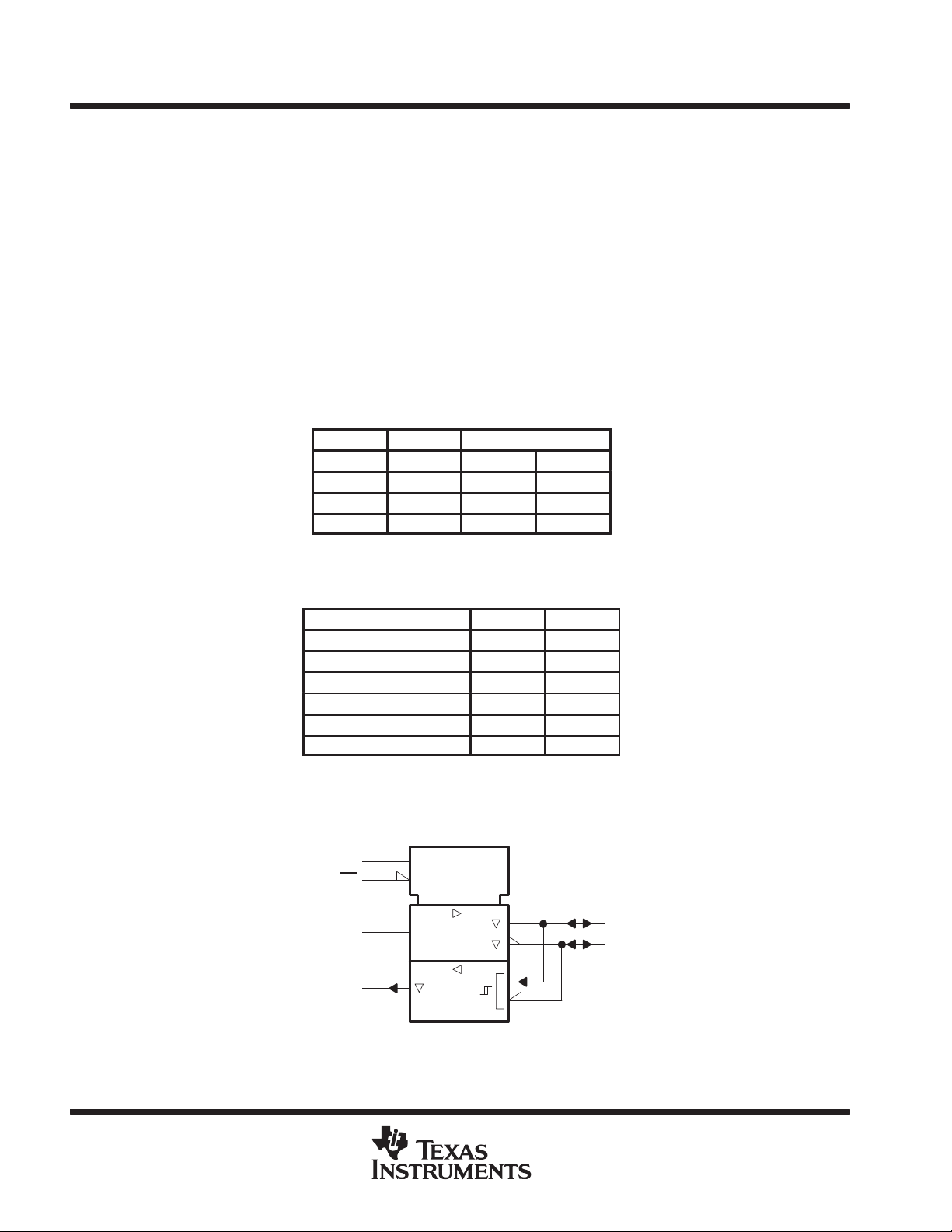
DRIVER FUNCTION TABLE
INPUT
D DE A B
H H H L
L H L H
X L Z Z
H = high level, L = low level, ? = indeterminate,
X = irrelevant, Z = high impedance (off)
ENABLE OUTPUTS
RECEIVER FUNCTION TABLE
DIFFERENTIAL INPUTS ENABLE OUTPUT
A – B RE R
VID ≥ 0.2 V L H
–0.2 V < VID < 0.2 V L ?
VID ≤ –0.2 V L L
X H Z
Open L H
H = high level, L = low level, ? = indeterminate,
X = irrelevant, Z = high impedance (off)
logic symbol
DE
RE
D
R
†
This symbol is in accordance with ANSI/IEEE Std 91-1984
and IEC Publication 617-12.
†
3
EN1
2
EN2
4
1
2
1
1
6
7
A
B
2
POST OFFICE BOX 655303 • DALLAS, TEXAS 75265
Page 3
SN65LBC184, SN75LBC184
PACKAGE
A
A
High-level output current, I
Low-level output current, I
mA
O erating free-air tem erature, T
A
DIFFERENTIAL TRANSCEIVER
WITH TRANSIENT VOLTAGE SUPPRESSION
SLLS236A – OCTOBER 1996 – REVISED MA Y 1998
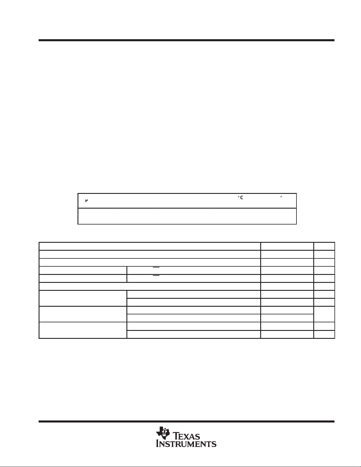
absolute maximum ratings over operating free-air temperature range (unless otherwise noted)
Supply voltage, V
Continuous voltage range at any bus terminal –15 V to 15 V. . . . . . . . . . . . . . . . . . . . . . . . . . . . . . . . . . . . . . . . .
Data input/output voltage –0.3 V to 7 V. . . . . . . . . . . . . . . . . . . . . . . . . . . . . . . . . . . . . . . . . . . . . . . . . . . . . . . . . . .
Electrostatic discharge:
Continuous total power dissipation (see Note 2) Internally Limited. . . . . . . . . . . . . . . . . . . . . . . . . . . . . . . . . . . . .
Operating free-air temperature range, T
Storage temperature range, T
Lead temperature 1,6 mm (1/16 inch) from case for 10 seconds 260°C. . . . . . . . . . . . . . . . . . . . . . . . . . . . . . .
†
Stresses beyond those listed under “absolute maximum ratings” may cause permanent damage to the device. These are stress ratings only, and
functional operation of the device at these or any other conditions beyond those indicated under “recommended operating conditions” is not
implied. Exposure to absolute-maximum-rated conditions for extended periods may affect device reliability.
NOTES: 1. All voltage values, except differential input/output bus voltage, are with respect to network ground terminal.
2. The driver shuts down at a junction temperature of approximately 160°C. To operate below this temperature, see the Dissipation
Rating Table.
3. GND and bus terminal ESD ratings are beyond readily available test equipment capabilities for MIL-STD-883C method 3015.3.
(see Note 1) –0.5 V to 7 V. . . . . . . . . . . . . . . . . . . . . . . . . . . . . . . . . . . . . . . . . . . . . . . . . . . .
CC
All Terminals (Class 3 A) (see Note 3) 8 kV. . . . . . . . . . . . . . . . . . . . . . . . . . . . . . . . . . .
All Terminals (Class 3 B) (see Note 3) 1200 V. . . . . . . . . . . . . . . . . . . . . . . . . . . . . . . . .
: SN65LBC184 – 40°C to 85°C. . . . . . . . . . . . . . . . . . . . . . . . . . . . . . .
A
SN75LBC184 0°C to 70°C. . . . . . . . . . . . . . . . . . . . . . . . . . . . . . . . .
–65°C to 150°C. . . . . . . . . . . . . . . . . . . . . . . . . . . . . . . . . . . . . . . . . . . . . . . . . . .
stg
DISSIPATION RATING TABLE
T
≤ 25°C DERATING FACTOR
POWER RATING ABOVE TA = 25°C
D 725 mW 5.8 mW/°C 464 mW 377 mW
P 1150 mW 9.2 mW/°C 736 mW 598 mW
T
= 70_C T
POWER RATINGAPOWER RATING
= 85_C
†
recommended operating conditions
MIN TYP MAX UNIT
Supply voltage, V
Voltage at any bus terminal (separately or common mode), VI or V
High-level input voltage, V
Low-level input voltage, V
Differential input voltage, |VID| 12 V
p
‡
The algebraic convention, in which the less-positive (more-negative) limit is designated minimum, is used in this data sheet for input voltage,
common-mode input voltage, common-mode output voltage, and free-air temperature levels only.
CC
IC
IH
IL
p
p
OH
OL
p
D, DE, and RE 2 V
D, DE, and RE 0.8 V
Driver –60 mA
Receiver –8 mA
Driver 60
Receiver 4
SN75LBC184 0 70 °C
SN65LBC184 –40
4.75 5 5.25 V
‡
–7
‡
12 V
85 °C
POST OFFICE BOX 655303 • DALLAS, TEXAS 75265
3
Page 4
SN65LBC184, SN75LBC184
,
mA
RE
A
Short-ci
t
(
)
(see Note 5)
voltage |V
A
VB| (see Note 4)
L
,
DIFFERENTIAL TRANSCEIVER
WITH TRANSIENT VOLTAGE SUPPRESSION
SLLS236A – OCTOBER 1996 – REVISED MA Y 1998
DRIVER SECTION
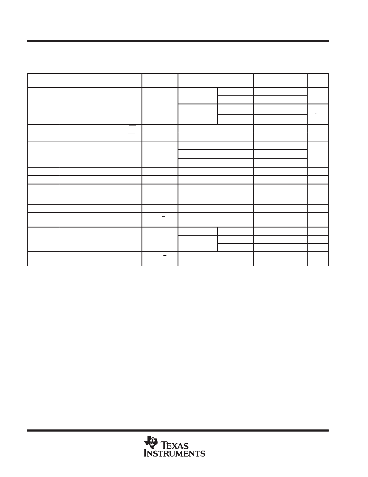
electrical characteristics over recommended operating conditions (unless otherwise noted)
PARAMETER
I
CC
I
IH
I
IL
I
OS
I
OZ
V
O
V
OC(PP)
V
OC
|∆V
OC(SS)
|VOD|
∆|VOD|
†
All typical values are measured with TA = 25°C and VCC = 5 V.
‡
IO = Iia, Iib. Iia and Iib are alternate symbols for input voltage.
NOTES: 4. The minimum VOD specification of the SN75LBC184 and the SN65LBC184 may not fully comply with ANSI RS-485 at operating
Supply current NA
High-level input current (D, DE, RE) NA VI = 2.4 V ±100 µA
Low-level input current (D, DE, RE) NA VI = 0.4 V ±100 µA
rcuit output curren
see Note 5
High-impedance output current NA See Receiver I
Output voltage Voa, V
Peak-to-peak change in common-
mode output voltage during state
transitions
Common-mode output voltage |Vos| See Figure 4 1 3 V
Magnitude of change, common-
|
mode steady-state output voltage
Magnitude of differential output
Change in differential voltage magnitude between logic states
temperature below 0°C. System designers should take the possibly lower output signal into account in determining the maximum
signal-transmission distance.
5. This parameter is measured with only one output being driven at a time.
–
–
ALTERNATE
SYMBOLS
NA
ob
NA
|Vos – Vos| See Figure 5 0.2 V
V
o
||Vt| – |Vt|| RL = 54 Ω 0.2 V
TEST CONDITIONS MIN
DE = RE = 5 V,
No Load
DE = 0 V,
= 5 V,
No Load
VO = –7 V –120 –250
VO = V
CC
VO = 12 V 250
‡
IO= 0
See Figures 5 and 6 0.8 V
IO = 0 1.5 6 V
R
= 54 Ω,
See Figure 4
SN75LBC184 12 25
SN65LBC184 12 30
SN75LBC184 175 300
SN65LBC184 175 300
TA ≥ 0°C 1.5 V
TA < 0°C 1 V
†
TYP
0 6 V
MAX UNIT
250
mA
I
mA
µ
4
POST OFFICE BOX 655303 • DALLAS, TEXAS 75265
Page 5

SN65LBC184, SN75LBC184
L
,
g
R
C
See Figure 5
DIFFERENTIAL TRANSCEIVER
WITH TRANSIENT VOLTAGE SUPPRESSION
SLLS236A – OCTOBER 1996 – REVISED MA Y 1998
DRIVER SECTION (CONTINUED)
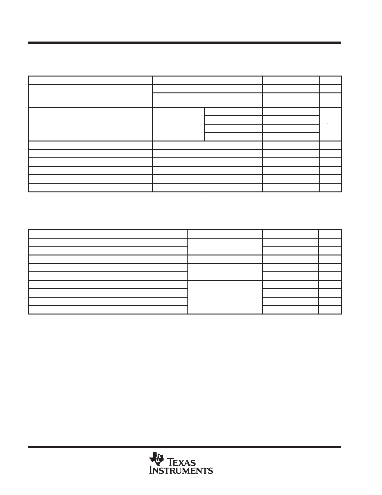
switching characteristics over recommended operating conditions (unless otherwise noted)
PARAMETER TEST CONDITIONS MIN TYP MAX UNIT
t
d(DH)
t
d(DL)
t
PLH
t
PHL
t
sk(p)
t
r
t
f
t
PZH
t
PZL
t
PHZ
t
PLZ
Differential output delay time, low-to-highlevel output
Differential-output delay time, high-to-lowlevel output
Propagation delay time, low-to-high-level
output
Propagation delay time, high-to-low-level
output
Pulse skew (|t
Rise time, single ended
Fall time, single ended
Output enable time to high level RL = 110 Ω, See Figure 2 3.5 µs
Output enable time to low level RL = 110 Ω, See Figure 3 3.5 µs
Output disable time from high level RL = 110 Ω, See Figure 2 2 µs
Output disable time from low level RL = 110 Ω, See Figure 3 2 µs
d(DH)
– t
|) 75 225 ns
d(DL)
R
= 54 Ω, See Figure 5
CL = 15 pF
= 54 Ω,
L
= 15 pF,
L
p
0.25 1.8 µs
0.25 1.8 µs
1.5 µs
1.5 µs
0.5 1.5 µs
0.5 1.5 µs
POST OFFICE BOX 655303 • DALLAS, TEXAS 75265
5
Page 6
SN65LBC184, SN75LBC184
IIInput current
Other input
V
A
C
50 pF
See Figure 7
See Figure 7
See Figure 8
DIFFERENTIAL TRANSCEIVER
WITH TRANSIENT VOLTAGE SUPPRESSION
SLLS236A – OCTOBER 1996 – REVISED MA Y 1998
RECEIVER SECTION
electrical characteristics over recommended operating conditions (unless otherwise noted)
PARAMETER TEST CONDITIONS MIN TYP†MAX UNIT
DE = RE = 0 V, No Load 3.9 mA
I
CC
I
OZ
V
V
V
V
V
†
All typical values are at VCC = 5 V, TA = 25°C.
‡
The algebraic convention, in which the less-positive (more-negative) limit is designated minimum, is used in this data sheet for input voltage,
common-mode input voltage, common-mode output voltage and free-air temperature levels only .
Supply current (total package)
p
High-impedance-state output current VO = 0.4 V to 2.4 V ±100 µA
Input hysteresis voltage 70 mV
hys
Positive-going input threshold voltage 200 mV
IT+
Negative-going input threshold voltage –200
IT–
High-level output voltage IOH = –8 mA Figure 7 2.7 V
OH
Low-level output voltage IOL = 4 mA Figure 7 0.5 V
OL
RE = 5 V,
No Load
DE = 0 V,
VI = 12 V 500
p
= 0
VI = 12 V, VCC = 0 500
VI = –7 V –400
VI = –7 V , VCC = 0 –400
‡
300 µA
µ
mV
switching characteristics over recommended operating conditions (unless otherwise noted)
PARAMETER TEST CONDITIONS MIN TYP MAX UNIT
t
PLH
t
PHL
t
sk(p)
t
r
t
f
t
PZH
t
PZL
t
PHZ
t
PLZ
Propagation delay time, low-to-high-level output
Propagation delay time, high-to-low-level output
Pulse skew (|t
Rise time, single ended
Fall time, single ended
Output enable time to high level 300 ns
Output enable time to low level
Output disable time from high level
Output disable time from low level 300 ns
pHL
– t
|) 100 ns
pLH
p
,
=
L
300 ns
300 ns
20 ns
20 ns
300 ns
300 ns
6
POST OFFICE BOX 655303 • DALLAS, TEXAS 75265
Page 7
SN65LBC184, SN75LBC184
DIFFERENTIAL TRANSCEIVER
WITH TRANSIENT VOLTAGE SUPPRESSION
SLLS236A – OCTOBER 1996 – REVISED MA Y 1998
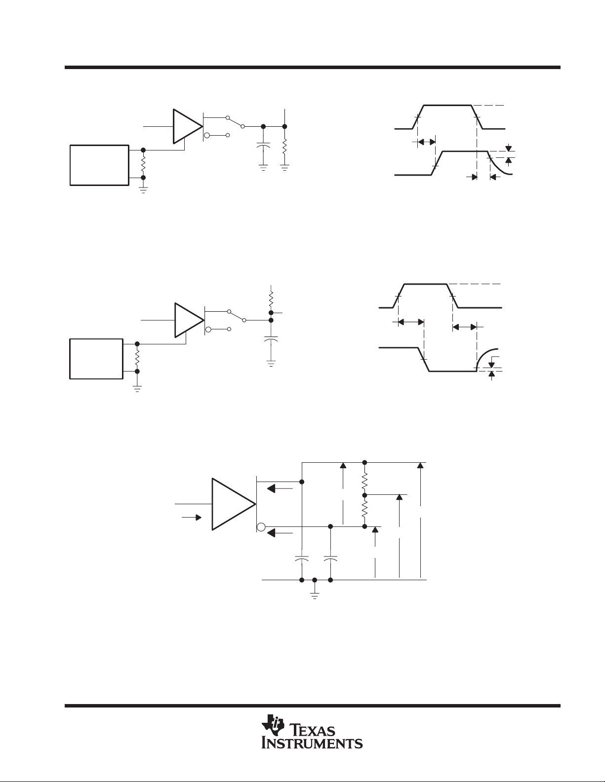
PARAMETER MEASUREMENT INFORMATION
Output
S1
0 or 3 V
CL = 50 pF
Generator
(see Note A)
NOTES: A. The input pulse is supplied by a generator having the following characteristics: PRR = 1.25 kHz, 50% duty cycle, tr ≤ 10 ns,
tf ≤ 10 ns, ZO = 50 Ω.
B. CL includes probe and jig capacitance.
50 Ω
Figure 2. Driver t
0 or 3 V
Generator
(see Note A)
50 Ω
(see Note B)
TEST CIRCUIT
CL = 50 pF
(see Note B)
PZH
S1
and t
PHZ
5 V
RL = 110 Ω
Output
RL = 110 Ω
Test Circuit and Voltage Waveforms
Input
Output
Input
Output
t
PZL
1.5 V
t
PZH
2.3 V
VOLTAGE WAVEFORMS
1.5 V
2.3 V
t
PHZ
1.5 V
1.5 V
t
PLZ
3 V
0 V
0.5 V
3 V
0 V
5 V
0.5 V
V
OL
V
OH
V
≈ 0 V
off
TEST CIRCUIT
NOTES: A. The input pulse is supplied by a generator having the following characteristics: PRR = 1.25 kHz, 50% duty cycle, tr ≤ 10 ns,
NOTES: A. Resistance values are in ohms and are 1% tolerance.
tf ≤ 10 ns, ZO = 50 Ω.
B. CL includes probe and jig capacitance.
Figure 3. Driver t
Input
B. CL includes probe and jig capacitance.
D
I
I
PZL
and t
I
I
Test Circuit and Voltage Waveforms
PLZ
A
V
O(A)
B
O(B)
C
L
OD
V
O(B)
C
L
VOLTAGE WAVEFORMS
27 Ω
27 Ω
V
O(A)
V
OC
Output
Figure 4. Driver Test Circuit, Voltage, and Current Definitions
POST OFFICE BOX 655303 • DALLAS, TEXAS 75265
7
Page 8

SN65LBC184, SN75LBC184
DIFFERENTIAL TRANSCEIVER
WITH TRANSIENT VOLTAGE SUPPRESSION
SLLS236A – OCTOBER 1996 – REVISED MA Y 1998
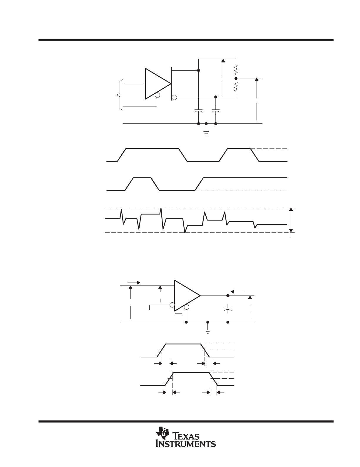
PARAMETER MEASUREMENT INFORMATION
Input
V
O(A)
V
O(B)
V
OD
t
PLH
50% 50%
10%
90% 90%
50% 50%
t
r
t
PHL
50% 50%
10%
t
r
t
d(DH)
10%
t
PHL
10%
t
t
PLH
90%90%
t
t
d(DL)
3 V
0 V
∼ 3.5 V
∼ 2.3 V
∼ 1 V
f
∼ 3.5 V
∼ 2.3 V
∼ 1 V
f
∼ 2.5 V
0 V
∼ –2.5 V
V
OC
Figure 5. Driver Timing, Voltage and Current Waveforms
∆V
OC(SS)
V
OC(PP)
8
POST OFFICE BOX 655303 • DALLAS, TEXAS 75265
Page 9
SN65LBC184, SN75LBC184
DIFFERENTIAL TRANSCEIVER
WITH TRANSIENT VOLTAGE SUPPRESSION
SLLS236A – OCTOBER 1996 – REVISED MA Y 1998
PARAMETER MEASUREMENT INFORMATION
Inputs
Output
Inputs
DE
D
DE
A
V
D
B
C
L
OD
C
L
27 Ω
27 Ω
Output
V
OC
3 V
0 V
3 V
0 V
NOTES: A. Resistance values are in ohms and are 1% tolerance.
NOTE A: This value includes probe and jig capacitance (± 10%).
B. CL includes probe and jig capacitance (± 10%).
Figure 6. Driver V
I
I
Input
V
I
Inputs
Output
Figure 7. Receiver t
t
PLH
1.5 V
PLH
A
B
OC(PP)
V
ID
10%
t
r
and t
50%
PHL
Test Circuit and Waveforms
I
t
PHL
t
O
Output
V
O
3 V
1.5 V
0 V
V
OH
50%
V
OL
f
RE
90%
R
50 pF
(see Note A)
50%
90%
10%
Test Circuit and Voltage Waveforms
V
OC(PP)
POST OFFICE BOX 655303 • DALLAS, TEXAS 75265
9
Page 10

SN65LBC184, SN75LBC184
DIFFERENTIAL TRANSCEIVER
WITH TRANSIENT VOLTAGE SUPPRESSION
SLLS236A – OCTOBER 1996 – REVISED MA Y 1998
PARAMETER MEASUREMENT INFORMATION
0 V or 3 V
1.5 V
Input
A
A
B
RE
R
50 pF
(see Note A)
3 V
0 V
5 V
620 Ω
620 Ω
V
O
Inputs
Output
NOTE A: This value includes probe and jig capacitance (± 10%).
RE
V
t
PHZ
O
1.5 V
0.5 V
Figure 8. Receiver t
t
PZH
PZL
, t
PLZ
, t
0.5 V
PZH
, and t
3 V
0 V
t
PLZ
V
OH
∼ 2.5 V
PHZ
0.5 V
Test Circuit and Voltage Waveforms
t
PZL
0.5 V
3 V
0 V
∼ 2.5 V
V
OL
10
POST OFFICE BOX 655303 • DALLAS, TEXAS 75265
Page 11

SN65LBC184, SN75LBC184
DIFFERENTIAL TRANSCEIVER
WITH TRANSIENT VOLTAGE SUPPRESSION
SLLS236A – OCTOBER 1996 – REVISED MA Y 1998
APPLICATION INFORMATION
’LBC184 test description
The ’LBC184 is tested against the CEI IEC 1000–4–5 recommended transient identified as the combination
wave. The combination wave provides a 1.2-/50-µs open-circuit voltage waveform and a 8-/20-µs short-circuit
current waveform shown in Figure 9. The testing is performed with a combination/hybrid pulse generator with
an effective output impedance of 2 Ω . The setup for the overvoltage stress is shown in Figure 10 with all testing
performed with power applied to the ’LBC184 circuit.
NOTE
High voltage transient testing is done on a sampling basis.
V
I(peak)
0.5 V
1.2 µs
P
tt
50 µs 20 µs
I
I(peak)
0.5 I
8 µs
P
Figure 9. Short-Circuit Current Waveforms
The ’LBC184 is tested and evaluated for both maximum (single pulse) as well as life test (multiple pulse)
capabilities. The ’LBC184 is evaluated against transients of both positive and negative polarity and all testing
is performed with the worst-case transient polarity . T ransient pulses are applied to the bus pins (A & B) across
ground as shown in Figure 10.
I
Key Tech
1.2/50 – 8/20
Combination Pulse
Generator
2-Ω Internal Impedance
High
Low
41.9 Ω
3 Ω
Current
Limiter
P
V
P
7
5
B/A
SN75LBC184
GND
Figure 10. Overvoltage-Stress Test Circuit
An example waveform as seen by the ’LBC184 is shown in Figure 1 1. The bottom trace is current, the middle
trace shows the clamping voltage of the device and the top trace is power as calculated from the voltage and
current waveforms. This example shows a peak clamping voltage of 16 V, peak current of 33.6 A yielding an
absorbed peak power of 538 W.
NOTE
A circuit reset may be required to ensure normal data communications following a transient noise
pulse of greater than 250 W peak.
POST OFFICE BOX 655303 • DALLAS, TEXAS 75265
11
Page 12

SN65LBC184, SN75LBC184
DIFFERENTIAL TRANSCEIVER
WITH TRANSIENT VOLTAGE SUPPRESSION
SLLS236A – OCTOBER 1996 – REVISED MA Y 1998
APPLICATION INFORMATION
Power
Clamping V oltage
Input Current
0
0
0
0204060
80 100 120 140 160 180
t – 20 µs/Div
Figure 11. Typical Surge Waveform Measured At Terminals 5 and 7
538 W Peak
16 V Peak,
V
I(peak)
33.6 A Peak,
I
I(peak)
12
POST OFFICE BOX 655303 • DALLAS, TEXAS 75265
Page 13

SN65LBC184, SN75LBC184
DIFFERENTIAL TRANSCEIVER
WITH TRANSIENT VOLTAGE SUPPRESSION
SLLS236A – OCTOBER 1996 – REVISED MA Y 1998
MECHANICAL INFORMATION
D (R-PDSO-G**) PLASTIC SMALL-OUTLINE PACKAGE
14 PIN SHOWN
14
1
0.069 (1,75) MAX
0.050 (1,27)
A
0.020 (0,51)
0.014 (0,35)
0.010 (0,25)
0.004 (0,10)
8
7
0.010 (0,25)
0.157 (4,00)
0.150 (3,81)
M
0.244 (6,20)
0.228 (5,80)
Seating Plane
0.004 (0,10)
PINS **
DIM
A MAX
A MIN
0.008 (0,20) NOM
Gage Plane
0°–8°
8
0.197
(5,00)
0.189
(4,80)
14
0.344
(8,75)
0.337
(8,55)
0.010 (0,25)
0.044 (1,12)
0.016 (0,40)
4040047/B 03/95
16
0.394
(10,00)
0.386
(9,80)
NOTES: A. All linear dimensions are in inches (millimeters).
B. This drawing is subject to change without notice.
C. Body dimensions do not include mold flash or protrusion, not to exceed 0.006 (0,15).
D. Four center pins are connected to die mount pad.
E. Falls within JEDEC MS-012
POST OFFICE BOX 655303 • DALLAS, TEXAS 75265
13
Page 14

SN65LBC184, SN75LBC184
DIFFERENTIAL TRANSCEIVER
WITH TRANSIENT VOLTAGE SUPPRESSION
SLLS236A – OCTOBER 1996 – REVISED MA Y 1998
MECHANICAL INFORMATION
P (R-PDIP-T8) PLASTIC DUAL-IN-LINE PACKAGE
0.400 (10,60)
0.355 (9,02)
58
0.260 (6,60)
0.240 (6,10)
41
0.070 (1,78) MAX
0.020 (0,51) MIN
0.200 (5,08) MAX
0.125 (3,18) MIN
0.100 (2,54)
0.021 (0,53)
0.015 (0,38)
NOTES: A. All linear dimensions are in inches (millimeters).
B. This drawing is subject to change without notice.
C. Falls within JEDEC MS-001
0.010 (0,25)
M
0.310 (7,87)
0.290 (7,37)
Seating Plane
0°–15°
0.010 (0,25) NOM
4040082/B 03/95
14
POST OFFICE BOX 655303 • DALLAS, TEXAS 75265
Page 15

IMPORTANT NOTICE
T exas Instruments and its subsidiaries (TI) reserve the right to make changes to their products or to discontinue
any product or service without notice, and advise customers to obtain the latest version of relevant information
to verify, before placing orders, that information being relied on is current and complete. All products are sold
subject to the terms and conditions of sale supplied at the time of order acknowledgement, including those
pertaining to warranty, patent infringement, and limitation of liability.
TI warrants performance of its semiconductor products to the specifications applicable at the time of sale in
accordance with TI’s standard warranty. Testing and other quality control techniques are utilized to the extent
TI deems necessary to support this warranty . Specific testing of all parameters of each device is not necessarily
performed, except those mandated by government requirements.
CERT AIN APPLICATIONS USING SEMICONDUCTOR PRODUCTS MAY INVOLVE POTENTIAL RISKS OF
DEATH, PERSONAL INJURY, OR SEVERE PROPERTY OR ENVIRONMENTAL DAMAGE (“CRITICAL
APPLICATIONS”). TI SEMICONDUCTOR PRODUCTS ARE NOT DESIGNED, AUTHORIZED, OR
WARRANTED TO BE SUITABLE FOR USE IN LIFE-SUPPORT DEVICES OR SYSTEMS OR OTHER
CRITICAL APPLICA TIONS. INCLUSION OF TI PRODUCTS IN SUCH APPLICATIONS IS UNDERST OOD TO
BE FULLY AT THE CUSTOMER’S RISK.
In order to minimize risks associated with the customer’s applications, adequate design and operating
safeguards must be provided by the customer to minimize inherent or procedural hazards.
TI assumes no liability for applications assistance or customer product design. TI does not warrant or represent
that any license, either express or implied, is granted under any patent right, copyright, mask work right, or other
intellectual property right of TI covering or relating to any combination, machine, or process in which such
semiconductor products or services might be or are used. TI’s publication of information regarding any third
party’s products or services does not constitute TI’s approval, warranty or endorsement thereof.
Copyright 1998, Texas Instruments Incorporated
 Loading...