

Datasheet SN65LBC180D, SN65LBC180DR, SN65LBC180N, SN75LBC180D, SN75LBC180DR Datasheet (Texas Instruments)
...
LOW-POWER DIFFERENTIAL LINE DRIVER AND RECEIVER PAIRS
D
Designed for High-Speed Multipoint Data
Transmission Over Long Cables
D
Operate With Pulse Durations as Low
as 30 ns
D
Low Supply Current ...5 mA Max
D
Meet or Exceed the Requirements of ANSI
Standard RS-485 and ISO 8482:1987(E)
D
3-State Outputs for Party-Line Buses
D
Common-Mode Voltage Range of
–7 V to 12 V
D
Thermal Shutdown Protection Prevents
Driver Damage From Bus Contention
D
Positive and Negative Output Current
Limiting
D
Pin Compatible With the SN75ALS180
description
The SN65LBC180 and SN75LBC180 differential
driver and receiver pairs are monolithic integrated
circuits designed for bidirectional data
communication over long cables that take on the
characteristics of transmission lines. They are
balanced, or differential, voltage mode devices
that meet or exceed the requirements of industry
standards ANSI RS-485 and ISO 8482:1987(E).
Both devices are designed using TI’s proprietary
LinBiCMOS with the low power consumption of
CMOS and the precision and robustness of
bipolar transistors in the same circuit.
SLLS174B – FEBRUARY 1994 – REVISED JANUARY 2000
GND
GND
NC–No internal connection
INPUT
D
H
L
X
DIFFERENTIAL INPUTS
A–B
VID ≥ 0.2 V
–0.2 V < VID < 0.2 V
VID ≤ – 0.2 V
X
Open circuit
H = high level,
Z = high impedance (off)
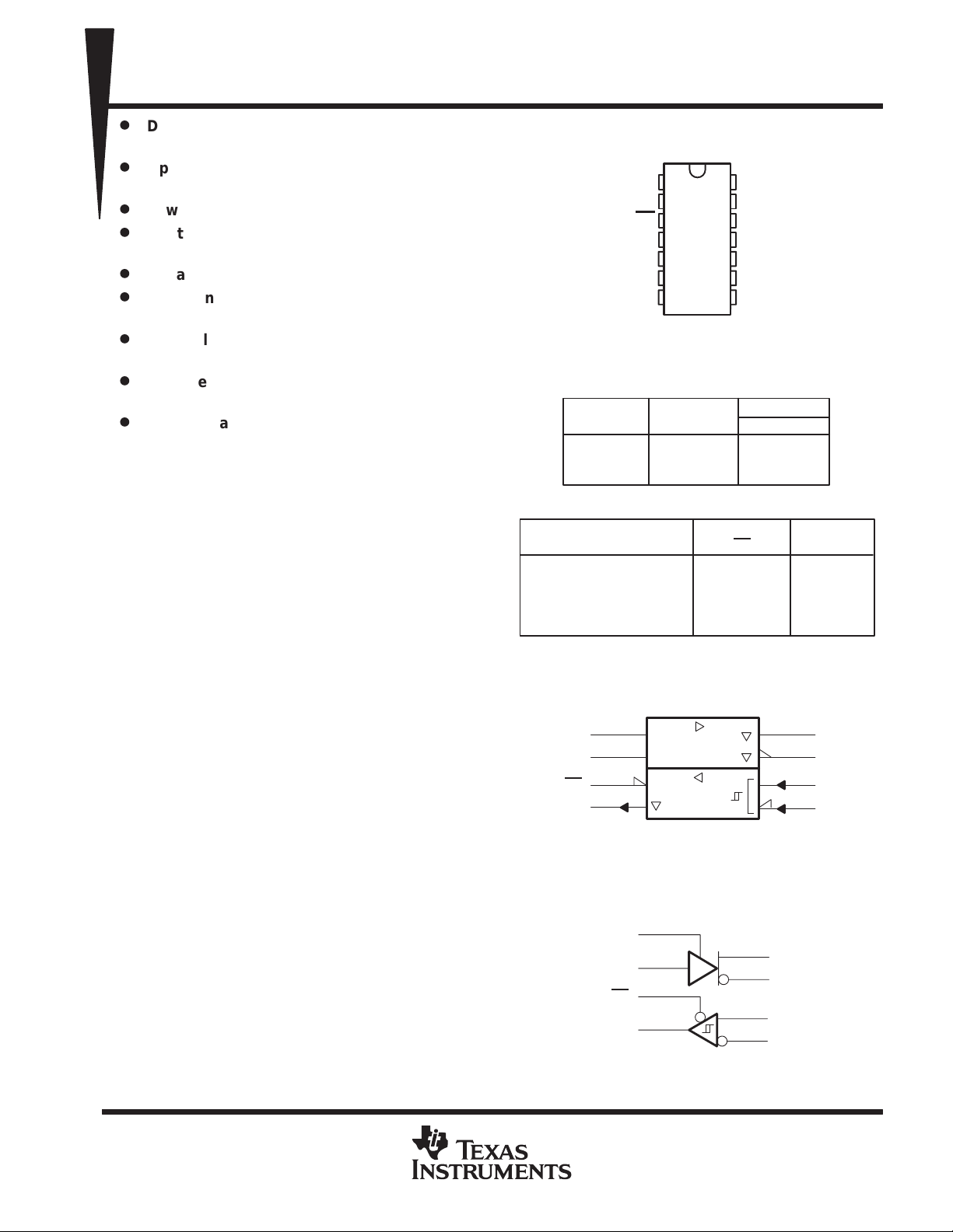
logic symbol
L =
†
SN65LBC180, SN75LBC180
D OR N PACKAGE
(TOP VIEW)
NC
1
R
2
RE
3
DE
4
D
5
6
7
Function Tables
DRIVER
ENABLE
DE
H
H
L
RECEIVER
low level, ? = indeterminate,
V
14
V
13
A
12
B
11
Z
10
Y
9
8
NC
ENABLE
RE
L
L
L
H
L
CC
CC
OUTPUTS
Y Z
H L
L H
Z Z
X =
OUTPUT
R
H
?
L
Z
H
irrelevant,
Both the SN65LBC180 and SN75LBC180
combine a differential line driver and receiver with
3-state outputs and operate from a single 5-V
supply. The driver and receiver have active-high
and active-low enables, respectively, which can
be externally connected to function as a direction
control. The driver differential outputs and the
receiver differential inputs are connected to
separate terminals for full-duplex operation and
are designed to present minimum loading to the
bus whether disabled or powered off (V
CC
These parts feature a wide common-mode
voltage range making them suitable for
point-to-point or multipoint data-bus applications.
LinBiCMOS is a trademark of Texas Instruments Incorporated.
PRODUCTION DATA information is current as of publication date.
Products conform to specifications per the terms of Texas Instruments
standard warranty. Production processing does not necessarily include
testing of all parameters.
= 0).
4
DE
5
D
3
RE
2
R
†
This symbol is in accordance with ANSI/IEEE Std 91-1984
and IEC Publication 617-12.
EN1
EN2
2
1
1
9
10
12
11
logic diagram (positive logic)
4
DE
5
D
3
RE
2
R
Copyright 2000, Texas Instruments Incorporated
10
12
11
9
Y
Z
A
B
Y
Z
A
B
POST OFFICE BOX 655303 • DALLAS, TEXAS 75265
1

SN65LBC180, SN75LBC180
LOW-POWER DIFFERENTIAL LINE DRIVER AND RECEIVER PAIRS
SLLS174B – FEBRUARY 1994 – REVISED JANUARY 2000
description (continued)
The devices also provide positive and negative output-current limiting and thermal shutdown for protection from
line fault conditions. The line driver shuts down at a junction temperature of approximately 172°C.
The SN65LBC180 and SN75LBC180 are available in the 14-pin dual-in-line and small-outline packages. The
SN75LBC180 is characterized for operation over the commercial temperature range of 0°C to 70°C. The
SN65LBC180 is characterized over the industrial temperature range of –40°C to 85°C.
schematics of inputs and outputs
RECEIVER A INPUTEQUIVALENT OF D, DE, AND RE INPUTS
V
CC
Input
100 kΩ
NOM
18 kΩ
NOM
3 kΩ
NOM
Input
22 kΩ
V
CC
Input
100 kΩ
NOM
RECEIVER B INPUT
V
CC
3 kΩ
18 kΩ
NOM
12 kΩ
NOM
1.1 kΩ
NOM
12 kΩ
1.1 kΩ
NOM
DRIVER OUTPUT TYPICAL OF RECEIVER OUTPUT
V
CC
Output
V
A Output
CC
2
POST OFFICE BOX 655303 • DALLAS, TEXAS 75265

High-level output current, I
mA
Low-level output current, I
mA
Operating free-air temperature, T
°C
SN65LBC180, SN75LBC180
LOW-POWER DIFFERENTIAL LINE DRIVER AND RECEIVER PAIRS
SLLS174B – FEBRUARY 1994 – REVISED JANUARY 2000
absolute maximum ratings over operating free-air temperature range (unless otherwise noted)
Supply voltage range, VCC (see Note 1) –0.3 V to 7 V. . . . . . . . . . . . . . . . . . . . . . . . . . . . . . . . . . . . . . . . . . . . . .
Input voltage range, VI (A, B)(see Note 1) –10 V to 15 V. . . . . . . . . . . . . . . . . . . . . . . . . . . . . . . . . . . . . . . . . . . . .
Voltage range at D, R, DE, RE (see Note 1) –0.3 V to VCC + 0.5 V. . . . . . . . . . . . . . . . . . . . . . . . . . . . . . . . . . .
Continuous total power dissipation (see Note 2) Internally limited. . . . . . . . . . . . . . . . . . . . . . . . . . . . . . . . . . . . . .
Total power dissipation See Dissipation Rating Table. . . . . . . . . . . . . . . . . . . . . . . . . . . . . . . . . . . . . . . . . . . . . . .
Operating free-air temperature range, T
: SN65LBC180 –40°C to 85°C. . . . . . . . . . . . . . . . . . . . . . . . . . . . . . .
A
SN75LBC180 0°C to 70°C. . . . . . . . . . . . . . . . . . . . . . . . . . . . . . . . .
Storage temperature range, T
–65°C to 150°C. . . . . . . . . . . . . . . . . . . . . . . . . . . . . . . . . . . . . . . . . . . . . . . . . . .
stg
Lead temperature 1,6 mm (1/16 inch) from case for 10 seconds 260°C. . . . . . . . . . . . . . . . . . . . . . . . . . . . . . .
†
Stresses beyond those listed under “absolute maximum ratings” may cause permanent damage to the device. These are stress ratings only, and
functional operation of the device at these or any other conditions beyond those indicated under “recommended operating conditions” is not
implied. Exposure to absolute-maximum-rated conditions for extended periods may affect device reliability.
NOTES: 1. All voltage values are with respect to GND.
2. The maximum operating junction temperature is internally limited. Use the dissipation rating table to operate below this temperature.
DISSIPATION RATING TABLE
PACKAGE
D 950 mW 7.6 mW/°C 608 mW 494 mW
N 1150 mW 9.2 mW/°C 736 mW 598 mW
TA ≤ 25°C
POWER RATING
DERATING FACTOR
ABOVE TA = 25°C
TA = 70°C
POWER RATING
TA = 85°C
POWER RATING
recommended operating conditions
MIN NOM MAX UNIT
Supply voltage, V
High-level input voltage, V
Low-level input voltage, V
Differential input voltage, V
Voltage at any bus terminal (separately or common mode), VO, VI, or V
p
‡
The algebraic convention where the least positive (more negative) limit is designated minimum, is used in this data sheet for the differential input
voltage, voltage at any bus terminal, operating temperature, input threshold voltage, and common-mode output voltage.
CC
IH
IL
ID
IC
p
p
OH
OL
p
A
D, DE, and RE 2 V
D, DE, and RE 0.8 V
A, B, Y, or Z –7
Y or Z –60
R –8
Y or Z 60
R 8
SN65LBC180 –40 85
SN75LBC180 0 70
4.75 5 5.25 V
‡
–6
‡
6 V
12 V
°
†
POST OFFICE BOX 655303 • DALLAS, TEXAS 75265
3
SN65LBC180, SN75LBC180
L
,
| V
|
gg
V
L
,
ICCSupply current
Receiver disabled
mA
R
See Figure 3
LOW-POWER DIFFERENTIAL LINE DRIVER AND RECEIVER PAIRS
SLLS174B – FEBRUARY 1994 – REVISED JANUARY 2000
DRIVER SECTION
electrical characteristics over recommended operating conditions (unless otherwise noted)
PARAMETER TEST CONDITIONS MIN TYP†MAX UNIT
V
IK
OD
∆| VOD |
V
OC
∆| VOC |
I
O
I
OZ
I
IH
I
IL
I
OS
†
All typical values are at VCC = 5 V and TA = 25°C.
NOTES: 3. The minimum VOD specification of the SN65LBC180 may not fully comply with ANSI RS-485 at operating temperatures below 0°C.
Input clamp voltage II = –18 mA –1.5 V
R
= 54 Ω,
Differential output voltage magnitude
(see Note 3)
Change in magnitude of differential output
voltage (see Note 4)
Common-mode output voltage 1 2.5 3 V
Change in magnitude of common-mode output
voltage (see Note 4)
Output current with power off VCC = 0, VO = –7 V to 12 V ±100 µA
High-impedance-state output current VO = –7 V to 12 V ±100 µA
High-level input current VI = 2.4 V –100 µA
Low-level input current VI = 0.4 V –100 µA
Short-circuit output current –7 V ≤ VO ≤ 12 V ±250 mA
pp
System designers should take the possibly lower output signal into account in determining the maximum signal-transmission
distance.
4. ∆|VOD| and ∆|VOC| are the changes in the steady-state magnitude of VOD and VOC, respectively, that occur when the input is
changed from a high level to a low level.
See Figure 1
= 60 Ω,
R
See Figure 2
See Figures 1 and 2 ±0.2 V
RL = 54 Ω, See Figure 1
SN65LBC180 1.1 2.5 5
SN75LBC180 1.5 2.5 5
SN65LBC180 1.1 2 5
SN75LBC180 1.5 2 5
±0.2 V
Outputs enabled 5
Outputs disabled 3
switching characteristics, VCC = 5 V, TA = 25°C
PARAMETER TEST CONDITIONS MIN TYP MAX UNIT
t
d(OD)
t
t(OD)
t
PZH
t
PZL
t
PHZ
t
PLZ
Differential output delay time
Differential output transition time
Output enable time to high level RL = 110 Ω, See Figure 4 35 ns
Output enable time to low level RL = 110 Ω, See Figure 5 35 ns
Output disable time from high level RL = 110 Ω, See Figure 4 50 ns
Output disable time from low level RL = 110 Ω, See Figure 5 35 ns
= 54 Ω,
L
7 12 18 ns
5 10 20 ns
4
POST OFFICE BOX 655303 • DALLAS, TEXAS 75265
IIBus input current
mA
ICCSupply current
Driver disabled
mA
V
S
6
See Figure 7
SN65LBC180, SN75LBC180
LOW-POWER DIFFERENTIAL LINE DRIVER AND RECEIVER PAIRS
SLLS174B – FEBRUARY 1994 – REVISED JANUARY 2000
RECEIVER SECTION
electrical characteristics over recommended operating conditions (unless otherwise noted)
PARAMETER TEST CONDITIONS MIN TYP MAX UNIT
V
Positive-going input threshold voltage IO = –8 mA 0.2 V
IT+
V
Negative-going input threshold voltage IO = 8 mA –0.2 V
IT–
V
Hysteresis voltage (V
hys
V
Enable-input clamp voltage II = –18 mA –1.5 V
IK
V
High-level output voltage VID = 200 mV, IOH = –8 mA 3.5 4.5 V
OH
V
Low-level output voltage VID = –200 mV, IOL = 8 mA 0.3 0.5 V
OL
I
High-impedance-state output current VO = 0 V to V
OZ
I
High-level enable-input current VIH = 2.4 V –50 µA
IH
I
Low-level enable-input current VIL = 0.4 V –100 µA
IL
p
pp
IT+
– V
) 45 mV
IT–
CC
VI = 12 V,
Other input at 0 V
VI = 12 V,
Other input at 0 V
VI = –7 V ,
Other input at 0 V
VI = –7 V ,
Other input at 0 V
VCC = 5 V,
VCC = 0 V,
VCC = 5 V,
VCC = 0 V,
Outputs enabled 5
Outputs disabled 3
0.7 1
0.8 1
–0.5 –0.8
–0.5 –0.8
±20 µA
switching characteristics, VCC = 5 V, TA = 25°C
PARAMETER TEST CONDITIONS MIN TYP MAX UNIT
t
Propagation delay time, high- to low-level output 11 22 33 ns
PHL
t
Propagation delay time, low- to high-level output
PLH
t
Pulse skew ( t
sk(p)
t
Transition time 5 8 ns
t
t
Output enable time to high level 35 ns
PZH
t
Output enable time to low level
PZL
t
Output disable time from high level
PHZ
t
Output disable time from low level 30 ns
PLZ
PHL
– t
PLH
)
ID
= –1.5 V to 1.5 V,
ee Figure
11 22 33 ns
3 6 ns
30 ns
35 ns
POST OFFICE BOX 655303 • DALLAS, TEXAS 75265
5
SN65LBC180, SN75LBC180
LOW-POWER DIFFERENTIAL LINE DRIVER AND RECEIVER PAIRS
SLLS174B – FEBRUARY 1994 – REVISED JANUARY 2000
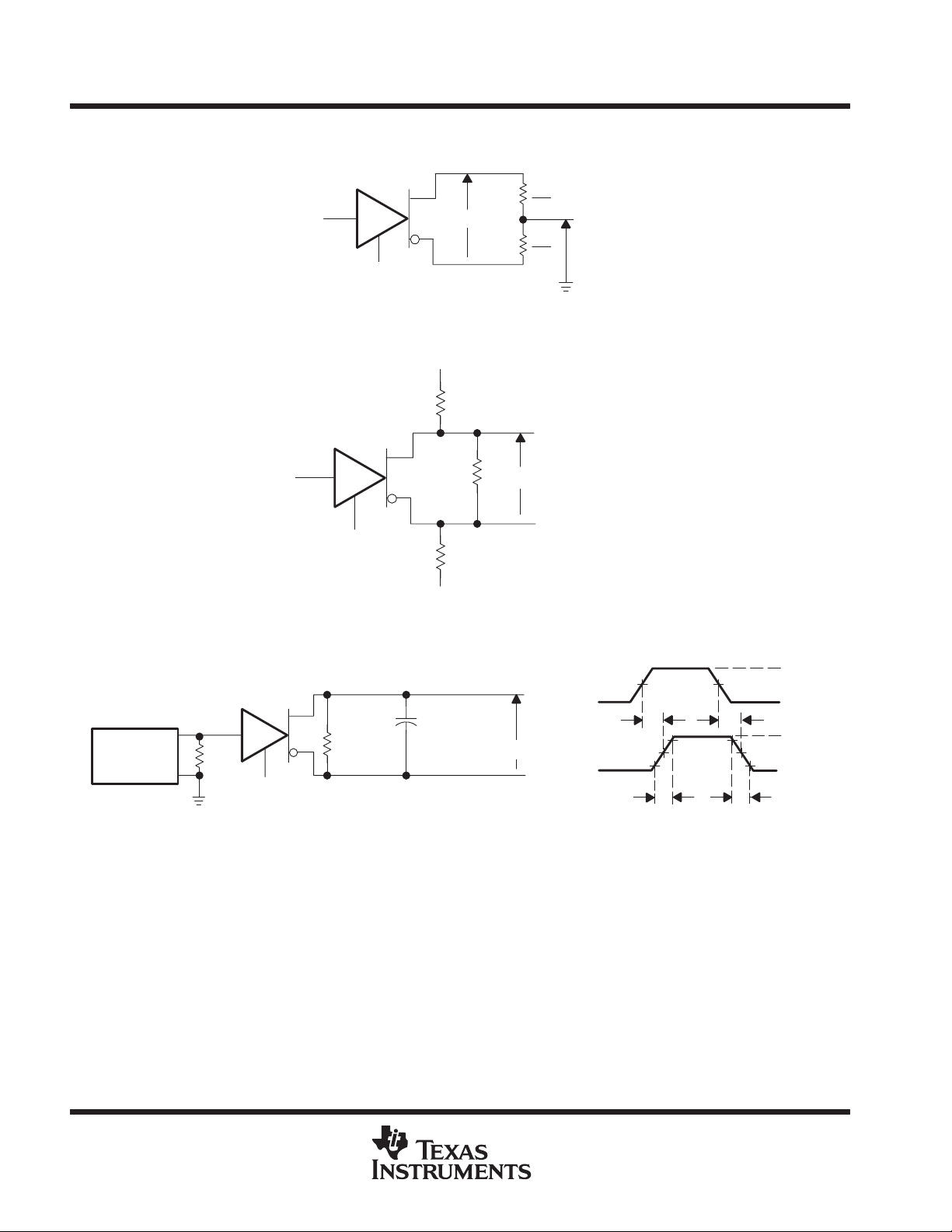
PARAMETER MEASUREMENT INFORMATION
Y
R
L
0 V or 3 V
D
DE at 3 V
V
OD
Z
Figure 1. Differential and Common-Mode Output Voltages
2
R
L
2
V
OC
Generator
(see Note A)
50 Ω
0 V or 3 V
DE at 3 V
D
DE at 3 V
V
test
RL = 60 Ω
V
test
–7 V < V
R1
375 Ω
R2
375 Ω
Figure 2. Driver VOD Test Circuit
CL = 50 pF
(see Note B)
RL = 54 Ω
Output
< 12 V
test
Y
V
OD
Z
50%
10%
3 V
0 V
t
d(OD)
≈ 2.5 V
≈ – 2.5 V
t
t(OD)
Input
Y
t
d(OD)
Output
Z
t
t(OD)
1.5 V
1.5 V 1.5 V
90%
50%
10%
90%
TEST CIRCUIT VOLTAGE WAVEFORMS
NOTES: A. The input pulse is supplied by a generator having the following characteristics: PRR > 1 MHz, 50% duty cycle, tr ≤ 6 ns, tf ≤ 6 ns,
ZO=50Ω.
B. CL includes probe and jig capacitance.
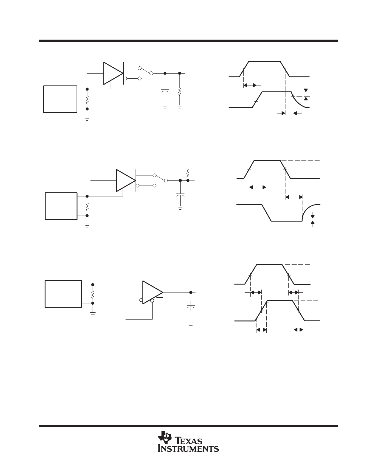
Figure 3. Driver Test Circuit and Differential Output Delay and Transition Time Voltage Waveforms
6
POST OFFICE BOX 655303 • DALLAS, TEXAS 75265
SN65LBC180, SN75LBC180
LOW-POWER DIFFERENTIAL LINE DRIVER AND RECEIVER PAIRS
SLLS174B – FEBRUARY 1994 – REVISED JANUARY 2000
PARAMETER MEASUREMENT INFORMATION
0 V or 3 V
Generator
(see Note A)
0 V or 3 V
Generator
(see Note A)
D
Input
50 Ω
DE
(see Note B)
TEST CIRCUIT
S1
Z
CL = 50 pF
Output
RL = 110 Ω
Input
Output
1.5 V
VOLTAGE WAVEFORMS
t
PZH
2.3 V
t
PHZ
1.5 V
Y
Figure 4. Driver Test Circuit and Enable and Disable Time Waveforms
5 V
Input
t
Output
PZL
2.3 V
50 Ω
D
Input
DE
Y
S1
Z
CL = 50 pF
(see Note B)
RL = 110 Ω
Output
3 V
0 V
0.5 V
V
OH
V
≈ 0
off
3 V
1.5 V1.5 V
0 V
t
PLZ
5 V
0.5 V
V
OL
TEST CIRCUIT VOLTAGE WAVEFORMS
Figure 5. Driver Test Circuit and Enable and Disable Time Voltage Waveforms
3 V
Input
Generator
(see Note A)
NOTES: A. The input pulse is supplied by a generator having the following characteristics: PRR ≤ 1 MHz, 50% duty cycle, tr ≤ 6 ns, tf ≤ 6 ns,
ZO=50Ω.
B. CL includes probe and jig capacitance.
50 Ω
1.5 V
0 V
TEST CIRCUIT VOLTAGE WAVEFORMS
A
R
B
RE
CL = 15 pF
(see Note B)
Output
Input
Output
t
PLH
1.3 V
10%
t
t
1.5 V
1.5 V
0 V
t
PHL
V
90%90%
1.3 V
10%
t
t
OH
V
OL
Figure 6. Receiver Test Circuit and Propagation Delay Time Voltage Waveforms
POST OFFICE BOX 655303 • DALLAS, TEXAS 75265
7

SN65LBC180, SN75LBC180
LOW-POWER DIFFERENTIAL LINE DRIVER AND RECEIVER PAIRS
SLLS174B – FEBRUARY 1994 – REVISED JANUARY 2000
PARAMETER MEASUREMENT INFORMATION
Input
Output
1.5 V
– 1.5 V
Generator
(see Note A)
S1
t
PZH
50 Ω
Input
1.5 V
A
B
3 V
0 V
RE
S1 to 1.5 V
S2 Open
S3 Closed
V
OH
1.5 V
0 V
Output
R
CL = 15 pF
(see Note B)
TEST CIRCUIT
Output
Input
5 kΩ
2 kΩ
IN916 or Equivalent
(4 places)
S3
t
PZL
S2
1.5 V
3 V
1.5 V
0 V
5 V
S1 to – 1.5 V
S2 Closed
S3 Open
≈ 4.5 V
V
OL
3 V
Input
t
PHZ
Output
1.5 V
0 V
S1 to 1.5 V
S2 Closed
S3 Closed
V
OH
Input
Output
t
PLZ
1.5 V
0.5 V
≈ 1.3 V
0.5 V
VOLTAGE WAVEFORMS
NOTES: A. The input pulse is supplied by a generator having the following characteristics: PRR ≤ 1 MHz, 50% duty cycle, tr ≤ 6 ns, tf ≤ 6 ns,
ZO=50Ω.
B. CL includes probe and jig capacitance.
3 V
S1 to – 1.5 V
S2 Closed
S3 Closed
0 V
≈ 1.3 V
V
OL
Figure 7. Receiver Output Enable and Disable Times
8
POST OFFICE BOX 655303 • DALLAS, TEXAS 75265

SN65LBC180, SN75LBC180
LOW-POWER DIFFERENTIAL LINE DRIVER AND RECEIVER PAIRS
SLLS174B – FEBRUARY 1994 – REVISED JANUARY 2000
TYPICAL CHARACTERISTICS
5
4.5
4
3.5
3
2.5
2
1.5
– High-Level Output Voltage – V
1
OH
V
0.5
0
DRIVER
HIGH-LEVEL OUTPUT VOLTAGE
vs
HIGH-LEVEL OUTPUT CURRENT
0102030
IOH – High-Level Output Current – mA
40 50 60
Figure 8
VCC = 5 V
TA = 25°C
70 80 90 100
LOW-LEVEL OUTPUT VOLTAGE
LOW-LEVEL OUTPUT CURRENT
5
VCC = 5 V
4.5
TA = 25°C
4
3.5
3
2.5
2
1.5
– Low-Level Output Voltage – V
1
OL
V
0.5
0
0204060
IOL – Low-Level Output Current – mA
DRIVER
vs
80 100 120
Figure 9
DIFFERENTIAL OUTPUT VOLTAGE
OUTPUT CURRENT
4
VCC = 5 V
TA = 25°C
3.5
3
2.5
2
1.5
– Differential Output Voltage – V
1
OD
V
0.5
0
0102030405060
IO – Output Current – mA
Figure 10
DRIVER
vs
70 80 90 100
DIFFERENTIAL OUTPUT VOLTAGE
3
VCC = 5 V
Load = 54 Ω
VIH = 2 V
2.5
2
1.5
1
– Differential Output Voltage – V
OD
V
0.5
0
– 50 – 25 0 25
TA – Free-Air Temperature – °C
DRIVER
vs
FREE-AIR TEMPERATURE
50 75
Figure 11
100 125
POST OFFICE BOX 655303 • DALLAS, TEXAS 75265
9

SN65LBC180, SN75LBC180
LOW-POWER DIFFERENTIAL LINE DRIVER AND RECEIVER PAIRS
SLLS174B – FEBRUARY 1994 – REVISED JANUARY 2000
TYPICAL CHARACTERISTICS
DIFFERENTIAL DELAY TIMES
20
VCC = 5 V
Load = 54 Ω
15
10
– Differential Delay Time – ns
5
d(OD)
t
0
– 50 – 25 0 25
DRIVER
vs
FREE-AIR TEMPERATURE
t
d(ODL)
t
d(ODH)
50 75
TA – Free-Air Temperature – °C
Figure 12
100 125
80
RL = 54 Ω
60
40
20
0
–20
– Output Current – mA
–40
O
I
–60
–80
0
VCC – Supply Voltage – V
DRIVER
OUTPUT CURRENT
vs
SUPPLY VOLTAGE
Figure 13
I
I
OL
OH
654321
HIGH-LEVEL OUTPUT VOLTAGE
HIGH-LEVEL OUTPUT CURRENT
6
5
4
3
2
– High-Level Output Voltage – V
1
OH
V
0
0 –10 – 20 – 30
IOH – High-Level Output Current – mA
RECEIVER
vs
Figure 14
VID = 200 mV
– 40 – 50
1
0.9
0.8
0.7
0.6
0.5
0.4
0.3
– Low-Level Output Voltage – V
0.2
OL
V
0.1
0
0510
RECEIVER
LOW-LEVEL OUTPUT VOLTAGE
vs
LOW-LEVEL OUTPUT CURRENT
VCC = 5 V
TA = 25°C
VID = – 200 mV
15 20 25
IOL – Low-Level Output Current – mA
Figure 15
30
35 40
10
POST OFFICE BOX 655303 • DALLAS, TEXAS 75265
SN65LBC180, SN75LBC180
LOW-POWER DIFFERENTIAL LINE DRIVER AND RECEIVER PAIRS
SLLS174B – FEBRUARY 1994 – REVISED JANUARY 2000
TYPICAL CHARACTERISTICS
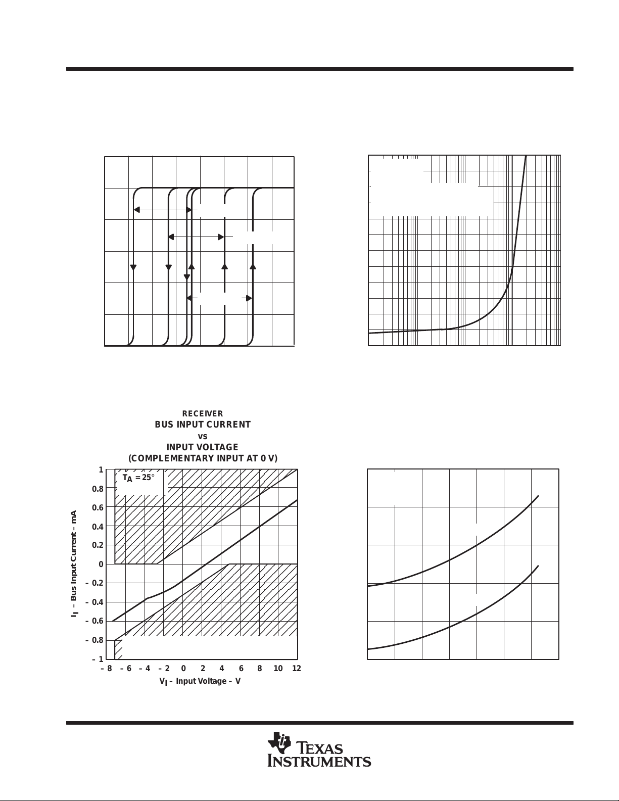
RECEIVER
OUTPUT VOLTAGE
vs
DIFFERENTIAL INPUT VOLTAGE
6
5
VIC = 12 V
4
VIC = 0 V
3
2
– Output Voltage – V
O
V
1
0
– 80 – 60 – 40 – 20 0 20 40 60 80
VID – Differential Input Voltage – mV
VIC = –7 V
Figure 16
AVERAGE SUPPLY CURRENT
vs
FREQUENCY
60
TA = 25°C
55
VCC = 5 V
50
DRVR and RCVR Enabled
Driver Load = Receiver Inputs
45
Receiver Load = 50 pF
40
35
30
25
20
– Average Supply Current – mAI
15
CC
10
5
0
10 k 100 k 1 M 10 M 100 M
f – Frequency – Hz
Figure 17
BUS INPUT CURRENT
(COMPLEMENTARY INPUT AT 0 V)
1
TA = 25°C
VCC = 5 V
0.8
0.6
0.4
0.2
0
– 0.2
– 0.4
– Bus Input Current – mA
I
I
– 0.6
– 0.8
– 1
The shaded region of this graph represents
more than 1 unit load per RS-485.
– 8 – 6 – 4 – 2 0 2
VI – Input Voltage – V
RECEIVER
vs
INPUT VOLTAGE
468
Figure 18
10 12
RECEIVER
PROPAGATION DELAY TIME
FREE-AIR TEMPERATURE
24.5
VCC = 5 V
CL = 15 pF
VIO = ±1.5 V
24
23.5
23
Propagation Delay Time – ns
22.5
22
– 40 – 20 0 20 40 60
TA – Free-Air Temperature – °C
Figure 19
vs
t
PHL
t
PLH
80 100
POST OFFICE BOX 655303 • DALLAS, TEXAS 75265
11

SN65LBC180, SN75LBC180
LOW-POWER DIFFERENTIAL LINE DRIVER AND RECEIVER PAIRS
SLLS174B – FEBRUARY 1994 – REVISED JANUARY 2000
APPLICATION INFORMATION
SN65LBC180
SN75LBC180
R
T
Up to 32
Unit Loads
• • •
NOTE A: The line should be terminated at both ends in its characteristic impedance (RT = ZO). Stub lengths off the main line should be kept
as short as possible. One SN75LBC180 typically represents less than one unit load.
R
T
SN65LBC180
SN75LBC180
Figure 20. Typical Application Circuit
12
POST OFFICE BOX 655303 • DALLAS, TEXAS 75265

SN65LBC180, SN75LBC180
LOW-POWER DIFFERENTIAL LINE DRIVER AND RECEIVER PAIRS
SLLS174B – FEBRUARY 1994 – REVISED JANUARY 2000
MECHANICAL DATA
D (R-PDSO-G**) PLASTIC SMALL-OUTLINE PACKAGE
14 PINS SHOWN
0.050 (1,27)
14
1
0.069 (1,75) MAX
A
0.020 (0,51)
0.014 (0,35)
0.010 (0,25)
0.004 (0,10)
DIM
8
7
PINS **
0.010 (0,25)
0.157 (4,00)
0.150 (3,81)
M
0.244 (6,20)
0.228 (5,80)
Seating Plane
0.004 (0,10)
8
14
0.008 (0,20) NOM
0°–8°
16
Gage Plane
0.010 (0,25)
0.044 (1,12)
0.016 (0,40)
A MAX
A MIN
NOTES: A. All linear dimensions are in inches (millimeters).
B. This drawing is subject to change without notice.
C. Body dimensions do not include mold flash or protrusion, not to exceed 0.006 (0,15).
D. Falls within JEDEC MS-012
POST OFFICE BOX 655303 • DALLAS, TEXAS 75265
0.197
(5,00)
0.189
(4,80)
0.344
(8,75)
0.337
(8,55)
0.394
(10,00)
0.386
(9,80)
4040047/D 10/96
13

SN65LBC180, SN75LBC180
LOW-POWER DIFFERENTIAL LINE DRIVER AND RECEIVER PAIRS
SLLS174B – FEBRUARY 1994 – REVISED JANUARY 2000
MECHANICAL DATA
N (R-PDIP-T**) PLASTIC DUAL-IN-LINE PACKAGE
16 PINS SHOWN
16
1
0.035 (0,89) MAX
PINS **
DIM
A
9
0.260 (6,60)
0.240 (6,10)
8
0.070 (1,78) MAX
0.020 (0,51) MIN
0.200 (5,08) MAX
A MAX
A MIN
Seating Plane
14
0.775
(19,69)
0.745
(18,92)
16
0.775
(19,69)
0.745
(18,92)
18
0.920
(23,37)
0.850
(21,59)
20
0.975
(24,77)
0.940
(23,88)
0.310 (7,87)
0.290 (7,37)
0.100 (2,54)
0.021 (0,53)
0.015 (0,38)
NOTES: A. All linear dimensions are in inches (millimeters).
B. This drawing is subject to change without notice.
C. Falls within JEDEC MS-001 (20-pin package is shorter than MS-001).
0.010 (0,25)
M
0.125 (3,18) MIN
0°–15°
0.010 (0,25) NOM
14/18 PIN ONL Y
4040049/C 08/95
14
POST OFFICE BOX 655303 • DALLAS, TEXAS 75265

IMPORTANT NOTICE
T exas Instruments and its subsidiaries (TI) reserve the right to make changes to their products or to discontinue
any product or service without notice, and advise customers to obtain the latest version of relevant information
to verify, before placing orders, that information being relied on is current and complete. All products are sold
subject to the terms and conditions of sale supplied at the time of order acknowledgement, including those
pertaining to warranty, patent infringement, and limitation of liability.
TI warrants performance of its semiconductor products to the specifications applicable at the time of sale in
accordance with TI’s standard warranty. Testing and other quality control techniques are utilized to the extent
TI deems necessary to support this warranty . Specific testing of all parameters of each device is not necessarily
performed, except those mandated by government requirements.
CERTAIN APPLICATIONS USING SEMICONDUCT OR PRODUCTS MAY INVOLVE POTENTIAL RISKS OF
DEATH, PERSONAL INJURY, OR SEVERE PROPERTY OR ENVIRONMENTAL DAMAGE (“CRITICAL
APPLICATIONS”). TI SEMICONDUCTOR PRODUCTS ARE NOT DESIGNED, AUTHORIZED, OR
WARRANTED TO BE SUITABLE FOR USE IN LIFE-SUPPORT DEVICES OR SYSTEMS OR OTHER
CRITICAL APPLICA TIONS. INCLUSION OF TI PRODUCTS IN SUCH APPLICATIONS IS UNDERST OOD TO
BE FULLY AT THE CUSTOMER’S RISK.
In order to minimize risks associated with the customer’s applications, adequate design and operating
safeguards must be provided by the customer to minimize inherent or procedural hazards.
TI assumes no liability for applications assistance or customer product design. TI does not warrant or represent
that any license, either express or implied, is granted under any patent right, copyright, mask work right, or other
intellectual property right of TI covering or relating to any combination, machine, or process in which such
semiconductor products or services might be or are used. TI’s publication of information regarding any third
party’s products or services does not constitute TI’s approval, warranty or endorsement thereof.
Copyright 2000, Texas Instruments Incorporated
 Loading...