

Datasheet SN65LBC031D, SN65LBC031DR, SN65LBC031P, SN65LBC031QD, SN65LBC031QDR Datasheet (Texas Instruments)
SN65LBC031Q
HIGH-SPEED CONTROLLER AREA NETWORK (CAN) TRANSCEIVERS
SLRS048B – MAY 1998 – REVISED MAY 2000
1
POST OFFICE BOX 655303 • DALLAS, TEXAS 75265
D
SN65LBC031Q Meets Standard ISO/DIS
11898 (up to 500 k Baud)
D
Driver Output Capability at 50 mA
D
Wide Positive and Negative Input/output
Bus Voltage Range
D
Bus Outputs Short-Circuit-Protected to
Battery Voltage and Ground
D
Thermal Shutdown
D
Available in Q-Temp Automotive
– High Reliability Automotive Applications
– Configuration Control/Print Support
– Qualification to Automotive Standards
description
The SN65LBC031Q is a CAN transceiver used as
an interface between a CAN controller and the
physical bus for high speed applications of up to
500 k Baud. The device provides transmit
capability to the differential bus and differential
receive capability to the controller. The transmitter
outputs (CANH and CANL), feature internal
transition regulation to provide controlled
symmetry resulting in low EMI emissions. Both
transmitter outputs are fully protected against battery short circuits and electrical transients that can occur on
the bus lines. In the event of excessive device power dissipation the output drivers are disabled by the thermal
shutdown circuitry at a junction temperature of approximately 160°C. The inclusion of an internal pullup resistor
on the transmitter input ensures a defined output during power up and protocol controller reset. For normal
operation at 500 k Baud the ASC terminal is open or tied to GND. For slower speed operation at 125 k Baud
the bus output transition times can be increased to reduce EMI by connecting the ASC terminal to V
CC
. The
receiver includes an integrated filter that suppresses the signal into pulses less than 30 ns wide.
The SN65LBC031Q is characterized for operation over the automotive temperature range of –40°C to 125°C.
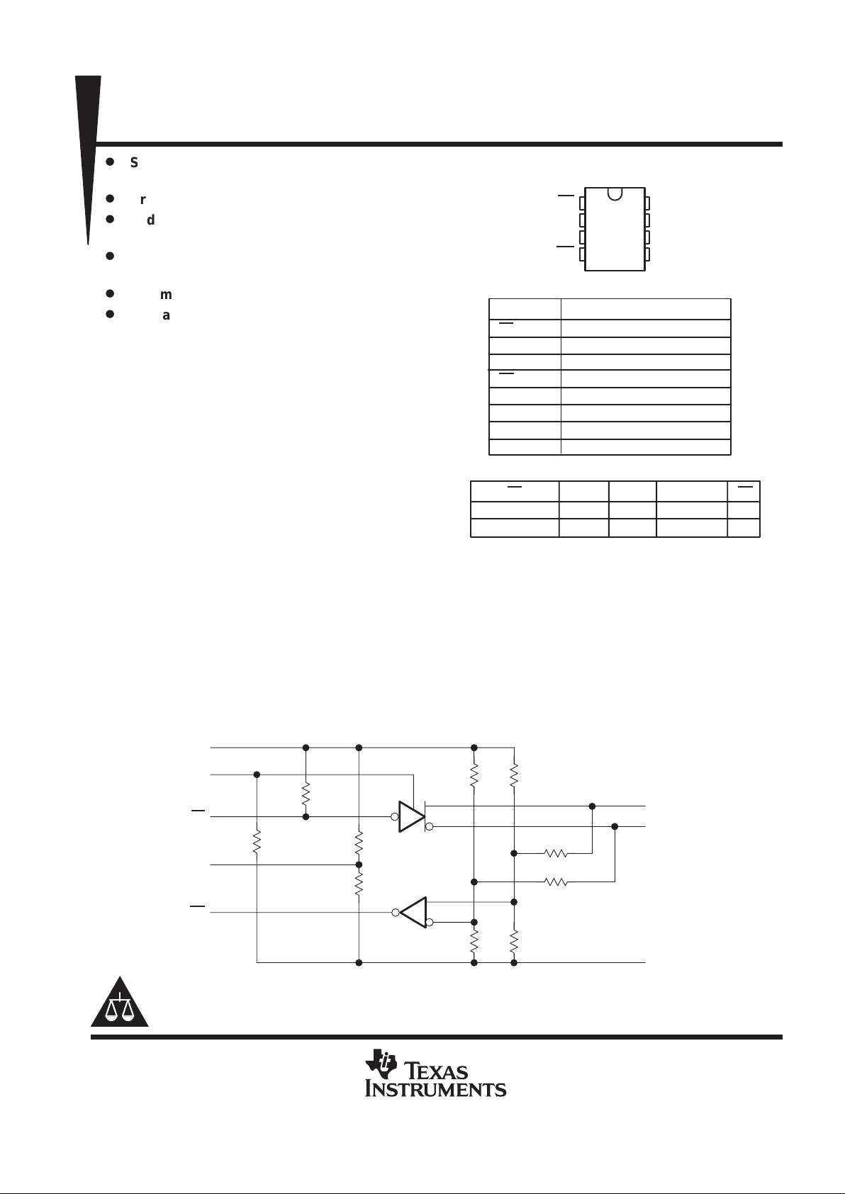
logic diagram
ASC
CANH
2R
2R
CANL
GND
V
CC
RX
REF
TX
RR
R2
R3
R1
R1
RR
Please be aware that an important notice concerning availability, standard warranty, and use in critical applications of
Texas Instruments semiconductor products and disclaimers thereto appears at the end of this data sheet.
Copyright 2000, Texas Instruments Incorporated
PRODUCTION DATA information is current as of publication date.
Products conform to specifications per the terms of Texas Instruments
standard warranty. Production processing does not necessarily include
testing of all parameters.
FUNCTION TABLE
TX
CANH
BUS STATE
CANL RX
L
High or floating
L = low, H = high
H
FloatingLFloating
L
H
Dominant
Recessive
1
2
3
4
8
7
6
5
TX
GND
V
CC
RX
ASC
CANH
CANL
REF
D PACKAGE
(TOP VIEW)
TERMINAL
TERMINAL FUNCTIONS
DESCRIPTION
TX
GND
RX
V
CC
REF
CANL
CANH
ASC
Transmitter input
Adjustable slope control
Ground
Supply voltage
Receiver output
Reference output
Low side bus output driver
High side bus output driver
SN65LBC031Q
HIGH-SPEED CONTROLLER AREA NETWORK (CAN) TRANSCEIVERS
SLRS048B – MAY 1998 – REVISED MAY 2000
2
POST OFFICE BOX 655303 • DALLAS, TEXAS 75265
absolute maximum ratings over operating free-air temperature range (unless otherwise noted)
†
Logic supply voltage, V
CC
(see Note 1) 7 V. . . . . . . . . . . . . . . . . . . . . . . . . . . . . . . . . . . . . . . . . . . . . . . . . . . . . . . .
Bus terminal voltage –5 V to 20 V. . . . . . . . . . . . . . . . . . . . . . . . . . . . . . . . . . . . . . . . . . . . . . . . . . . . . . . . . . . . . . . . .
Input current at TX and ASC terminal, II ±10 mA. . . . . . . . . . . . . . . . . . . . . . . . . . . . . . . . . . . . . . . . . . . . . . . . . . . .
Input voltage at TX
and ASC terminal, VI 2 × V
CC
. . . . . . . . . . . . . . . . . . . . . . . . . . . . . . . . . . . . . . . . . . . . . . . . . . .
Operating free-air temperature range, TA –40°C to125°C. . . . . . . . . . . . . . . . . . . . . . . . . . . . . . . . . . . . . . . . . .
Operating junction temperature range, TJ –40°C to 150°C. . . . . . . . . . . . . . . . . . . . . . . . . . . . . . . . . . . . . . . . . . .
Continuous total power dissipation at (or below) 25°C free-air temperature See Dissipation Rating Table. .
Storage temperature range, T
stg
–65°C to 150°C. . . . . . . . . . . . . . . . . . . . . . . . . . . . . . . . . . . . . . . . . . . . . . . . . . .
Case temperature for 10 sec TC, D package 260°C. . . . . . . . . . . . . . . . . . . . . . . . . . . . . . . . . . . . . . . . . . . . . . . .
†
Stresses beyond those listed under “absolute maximum ratings” may cause permanent damage to the device. These are stress ratings only, and
functional operation of the device at these or any other conditions beyond those indicated under “recommended operating conditions” is not
implied. Exposure to absolute-maximum-rated conditions for extended periods may affect device reliability.
NOTE 1: All voltage values, except differential bus voltage, are measured with respect to GND.
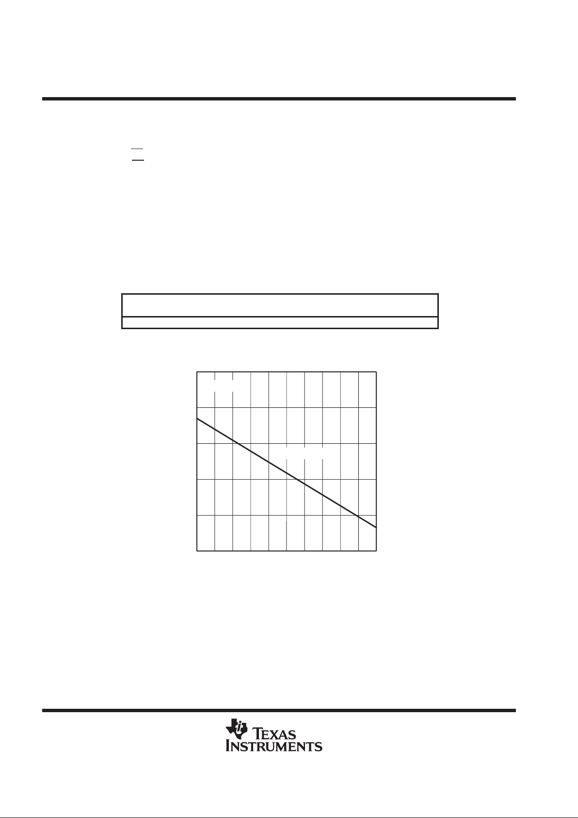
DISSIPATION RATING TABLE
PACKAGE
TA ≤ 25°C
POWER RATING
OPERATING FACTOR
ABOVE TC = 25°C
TC = 125°C
POWER RATING
D 725 mW 5.8 mW/°C 145 mW
800
400
0
25 45 65 85
– Maximum Continuous Dissipation – mW
DISSIPATION DERATING CURVE
vs
FREE-AIR TEMPERATURE
105 125
1000
600
200
P
D
TA – Free-Air Temperature – °C
TC = 25°C
35 55 75 95 115
D = 5.8 mW/°C
Figure 1
SN65LBC031Q
HIGH-SPEED CONTROLLER AREA NETWORK (CAN) TRANSCEIVERS
SLRS048B – MAY 1998 – REVISED MAY 2000
3
POST OFFICE BOX 655303 • DALLAS, TEXAS 75265
recommended operating conditions
MIN NOM MAX UNIT
Logic supply voltage, V
CC
4.5 5 5.5 V
Voltage at any bus terminal (separately or common mode), VI or VIC (see Note 3) –2 7 V
High-level input voltage, V
IH
TX 2 V
CC
V
Low-level input voltage, V
IL
TX 0 0.8 V
p
Transmitter –50 mA
High-level output current, I
OH
Receiver –400 µA
p
Transmitter 50
Low-level output current, I
OL
Receiver 1
mA
Operating free-air temperature, T
A
–40 125 °C
NOTES: 2. All voltage values, except differential bus voltage, are measured with respect to the ground terminal.
3. For bus voltages from –5 V to –2 V and 7 V to 20 V the receiver output is stable.
SYMBOL DEFINITION
DATA SHEET PARAMETER
DEFINITION
V
O(CANHR)
CANH bus output voltage (recessive state)
V
O(CANLR)
CANL bus output voltage (recessive state)
V
O(CANHD)
CANH bus output voltage (dominant state)
V
O(CANLD)
CANL bus output voltage (dominant state)
V
O(DIFFR)
Bus differential output voltage (recessive state)
V
O(DIFFD)
Bus differential output voltage (dominant state)
V
I(ASC)
Adjustable slope control input voltage
electrical characteristics over recommended ranges of supply voltage and operating free-air
temperature (unless otherwise noted)
PARAMETER TEST CONDITIONS MIN TYP MAX UNIT
V
O(REF)
Reference source output voltage I
REF
= ±20 µA 0.45V
CC
0.55V
CC
V
R
O(REF)
Reference source output resistance 5 10 kΩ
I
CC(REC)
Logic supply current, recessive state
12 20
I
CC(DOM)
Logic supply current, dominant state
See Figure 2
, S1
closed
55 80
mA

SN65LBC031Q
HIGH-SPEED CONTROLLER AREA NETWORK (CAN) TRANSCEIVERS
SLRS048B – MAY 1998 – REVISED MAY 2000
4
POST OFFICE BOX 655303 • DALLAS, TEXAS 75265
transmitter electrical characteristics over recommended ranges of supply and operating free-air
temperature (unless otherwise noted)
PARAMETER TEST CONDITIONS MIN TYP MAX UNIT
V
O(CANHR)
V
O(CANLR)
Output voltage (recessive state)
See Figure 2, S1 open
2 0.5V
CC
3 V
V
O(DIFFR)
Differential output voltage (recessive state)
g,
–500 0 50 mV
V
O(CANHD)
Output voltage (dominant state) 2.75 3.5 4.5
V
O(CANLD)
Output voltage (dominant state)
See Figure 2, S1 closed
0.5 1.5 2.25
V
V
O(DIFFD)
Differential output voltage (dominant state) 1.5 2 3
p
VIH = 2.4 V –100 –185
I
IH(TX)
High-level input current (TX)
VIH = V
CC
±2
µ
A
p
VIH = 2.4 V 100 165
I
IH(ASC)
High-level input current (ASC)
VIH = V
CC
200 340
µ
A
I
IL(TX)
Low-level input current (TX) VIL = 0.4 V –180 –400 µA
I
IL(ASC)
Low-level input current (ASC) VIL = 0.4 V 15 25 µA
C
I(TX)
TX input capacitance 8 pF
I
O(ssH)
CANH short circuit output current V
O(CANH)
= –2 V to 20 V –95 –200 mA
I
O(ssL)
CANL short circuit output current V
O(CANL)
= 20 V to –2 V 140 250 mA
NOTE 2: All voltage values, except differential bus voltage, are measured with respect to the ground terminal.
transceiver dynamic characteristics over recommended operating free-air temperature range and
V
CC
= 5 V
PARAMETER TEST CONDITIONS MIN TYP MAX UNIT
p
See Figures 2 and 3,
S1 closed,
V
I(ASC)
= 0 V or open circuit,
S2 open
280 ns
t
(loop)
Loop time
See Figures 2 and 3,
S1 closed,
V
I(ASC)
= VCC,
S2 closed
400 ns
Differential-output slew rate
See Figures 2 and 4,
S1 closed,
V
I(ASC)
= 0 or open circuit,
S2 open
35 V/µs
SR
(RD)
(recessive to dominant)
See Figures 2 and 4,
S1 closed,
V
I(ASC)
= VCC,
S2 closed
10 V/µs
Differential-output slew rate
See Figures 2 and 4,
S1 closed,
V
I(ASC)
= 0 or open circuit,
S2 open
10 V/µs
SR
(DR)
(dominant to recessive)
See Figures 2 and 4,
S1 closed,
V
I(ASC)
= VCC,
S2 closed
10 V/µs
t
d(RD)
p
55 ns
t
d(DR)
Differential-output delay time
See Figure 2
,
S1 closed
160 ns
t
pd(RECRD)
Receiver propagation delay
90 ns
t
pd(RECDR)
gy
time
See Figures 2 and 5
55 ns
NOTE 4: Receiver input pulse width should be >50 ns. Input pulses of <30 ns are suppressed.

SN65LBC031Q
HIGH-SPEED CONTROLLER AREA NETWORK (CAN) TRANSCEIVERS
SLRS048B – MAY 1998 – REVISED MAY 2000
5
POST OFFICE BOX 655303 • DALLAS, TEXAS 75265
receiver electrical characteristics over recommended ranges of common-mode input voltage,
supply voltage, and operating free-air temperature (unless otherwise noted)
PARAMETER TEST CONDITIONS MIN TYP MAX UNIT
V
IT(REC)
Differential input threshold voltage for recessive state
500
V
IT(DOM)
Differential input threshold voltage for dominant state
V
IC
= –
2 V to 7 V
900
mV
V
hys
Recessive-dominant input hysteresis 100 180 mV
V
OH(RX)
High-level output voltage
V
O(DIFF)
= 500 mV ,
IOH = –400 µA
VCC–0.5 V V
CC
V
V
OL(RX)
Low-level output voltage
V
O(DIFF)
= 900 mV ,
IOL = 1 mA
0 0.5 V
r
I(REC)
CANH and CANL input resistance in recessive state dc, no load 5 50 kΩ
r
I(DIFF)
Differential CANH and CANL input resistance in recessive
state
dc, no load 10 100 kΩ
C
i
CANH and CANL input capacitance 20 pF
C
i(DHL)
Differential CANH and CANL input capacitance 10 pF
NOTE 2: All voltage values, except differential bus voltage, are measured with respect to the ground terminal.
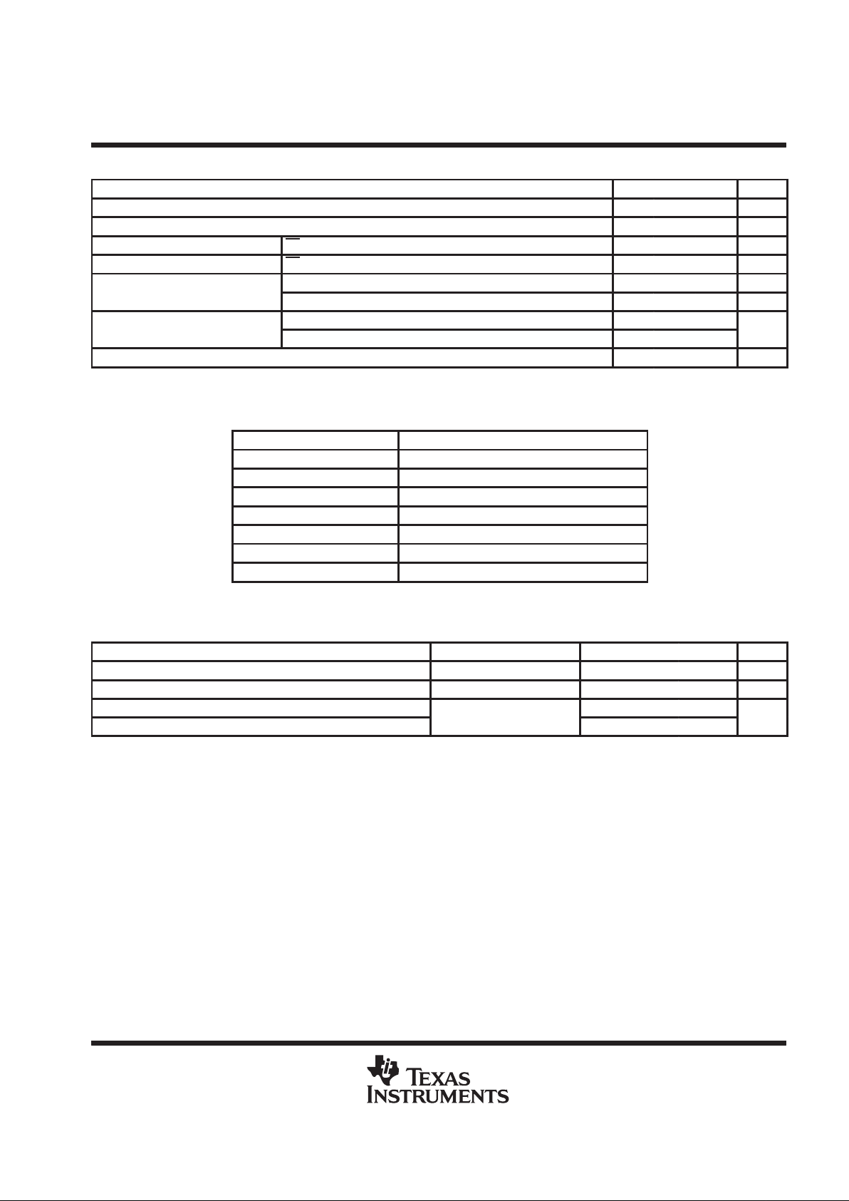
PARAMETER MEASUREMENT INFORMATION
CANH
CANL
V
CC
TX
Input
60 Ω 60 Ω
60 Ω 60 Ω
R
Generator
(see Note A)
RX Output
ASC
V
DIFF
56 pF
15 pF
56 pF
S2
S1
NOTE A: The input pulse is supplied to TX by a generator having a tr and tf = 5 ns.
Figure 2. Test Circuit

SN65LBC031Q
HIGH-SPEED CONTROLLER AREA NETWORK (CAN) TRANSCEIVERS
SLRS048B – MAY 1998 – REVISED MAY 2000
6
POST OFFICE BOX 655303 • DALLAS, TEXAS 75265
PARAMETER MEASUREMENT INFORMATION
t
loop
TX Input
RX
Output
10%
90%
1.5 V
3 V
0 V
V
OH
V
OL
t
loop
Figure 3. Loop Time
SR(RD)
TX Input
V
O(DIFF)
80%
20%
1.5 V
3 V
0 V
V
OH
V
OL
SR(DR)
80%
20%
Figure 4. Slew Rate
NOTE A: The input pulse is supplied to TX by a generator having a tr and tf = 5 ns.
NOTE A: The input pulse is supplied as V
DIFF
using CANH and CANL
respectively by a generator having a tr and tf = 5 ns.
t
pd(RECRD)
RX Output
V
O(DIFF)
10%
90%
0.9 V
t
pd(RECDR)
0.5 V
Figure 5. Receiver Delay Times
V
S
100 pF
100 pF
60 Ω
CANH
CANL
R
(SOURCE)
Transient Source
(Schaffner Generator)
Figure 6. Transient Stress Capability Test Circuit

SN65LBC031Q
HIGH-SPEED CONTROLLER AREA NETWORK (CAN) TRANSCEIVERS
SLRS048B – MAY 1998 – REVISED MAY 2000
7
POST OFFICE BOX 655303 • DALLAS, TEXAS 75265
PARAMETER MEASUREMENT INFORMATION
V
S
Transient Magnitude
vs
Time
90%
10%
0 V
t
r
t
d
t
2
t
1
– Transient Magnitude – %V
S
t – Time
Figure 7. Transient Stress Capability Waveform
Table 1. Test Circuit Results According to DIN 40839
TEST PULSE
TRANSIENT
MAGNITUDE
V
S
SOURCE
IMPEDANCE
R
SOURCE
PULSE WIDTH
td
(see Note 5)
PULSE RISE
TIME, tr
(see Note 6)
PULSE TIME,
t
2
(see Figure 7)
REPETITION
PERIOD, t
1
(see Figure 7)
NUMBER OF
PULSES
1 –100 V 10 Ω 2 ms 1 µs 200 ms 5 s 5000
2 100 V 10 Ω 50 µs 1 µs 200 ms 5 s 5000
3a –150 V 50 Ω 0.1 µs 5 ns 100 µs 100 µs See Note 7
3b 100 V 50 Ω 0.1 µs 5 ns 100 µs 100 µs See Note 7
5 60 V 1 Ω 400 ms 5 ms — — 1
NOTES: 5. Measured from 10% on rising edge to 10% on falling edge
6. Measured from 10% to 90% of pulse
7. Pulse package for a period of 3600 s, 10 ms pulse time, 90 ms stop time
SN65LBC031Q
HIGH-SPEED CONTROLLER AREA NETWORK (CAN) TRANSCEIVERS
SLRS048B – MAY 1998 – REVISED MAY 2000
8
POST OFFICE BOX 655303 • DALLAS, TEXAS 75265
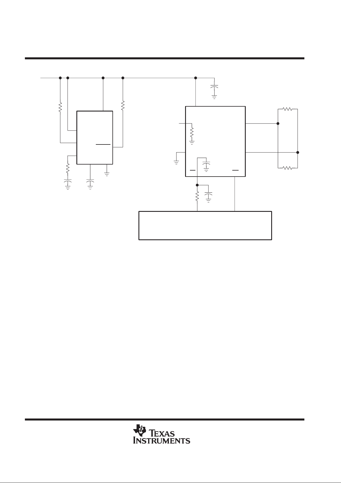
APPLICATION INFORMATION
154
3
6
7
2
8
GND
ASC
V
CC
5
3
C
t
2
RESIN
7
SENSE
RESET
V
CC
10 kΩ
REF GND
8
14
0.1 µF
5 V
CANH
CANL
REF
RX
100 nF
TL7705B
SN65LBC031Q
TX
C
in
CAN Microcontroller
120 Ω
120 Ω
10 kΩ
Figure 8. T ypical SN65LBC031Q Application

SN65LBC031Q
HIGH-SPEED CONTROLLER AREA NETWORK (CAN) TRANSCEIVERS
SLRS048B – MAY 1998 – REVISED MAY 2000
9
POST OFFICE BOX 655303 • DALLAS, TEXAS 75265
MECHANICAL DATA
D (R-PDSO-G**) PLASTIC SMALL-OUTLINE PACKAGE
14 PIN SHOWN
4040047/D 10/96
0.228 (5,80)
0.244 (6,20)
0.069 (1,75) MAX
0.010 (0,25)
0.004 (0,10)
1
14
0.014 (0,35)
0.020 (0,51)
A
0.157 (4,00)
0.150 (3,81)
7
8
0.044 (1,12)
0.016 (0,40)
Seating Plane
0.010 (0,25)
PINS **
0.008 (0,20) NOM
A MIN
A MAX
DIM
Gage Plane
0.189
(4,80)
(5,00)
0.197
8
(8,55)
(8,75)
0.337
14
0.344
(9,80)
16
0.394
(10,00)
0.386
0.004 (0,10)
M
0.010 (0,25)
0.050 (1,27)
0°–8°
NOTES: A. All linear dimensions are in inches (millimeters).
B. This drawing is subject to change without notice.
C. Body dimensions do not include mold flash or protrusion, not to exceed 0.006 (0,15).
D. Falls within JEDEC MS-012

IMPORTANT NOTICE
T exas Instruments and its subsidiaries (TI) reserve the right to make changes to their products or to discontinue
any product or service without notice, and advise customers to obtain the latest version of relevant information
to verify, before placing orders, that information being relied on is current and complete. All products are sold
subject to the terms and conditions of sale supplied at the time of order acknowledgment, including those
pertaining to warranty, patent infringement, and limitation of liability.
TI warrants performance of its semiconductor products to the specifications applicable at the time of sale in
accordance with TI’s standard warranty. T esting and other quality control techniques are utilized to the extent
TI deems necessary to support this warranty. Specific testing of all parameters of each device is not necessarily
performed, except those mandated by government requirements.
Customers are responsible for their applications using TI components.
In order to minimize risks associated with the customer’s applications, adequate design and operating
safeguards must be provided by the customer to minimize inherent or procedural hazards.
TI assumes no liability for applications assistance or customer product design. TI does not warrant or represent
that any license, either express or implied, is granted under any patent right, copyright, mask work right, or other
intellectual property right of TI covering or relating to any combination, machine, or process in which such
semiconductor products or services might be or are used. TI’s publication of information regarding any third
party’s products or services does not constitute TI’s approval, warranty or endorsement thereof.
Copyright 2000, Texas Instruments Incorporated
 Loading...