

Page 1

SN55461 THRU SN55463
SN75461 THRU SN75463
DUAL PERIPHERAL DRIVERS
SLRS022A – DECEMBER 1976 – REVISED OCT OBER 1995
PERIPHERAL DRIVERS FOR
HIGH-VOLTAGE, HIGH-CURRENT DRIVER
APPLICATIONS
• Characterized for Use to 300 mA
• High-Voltage Outputs
• No Output Latch-Up at 30 V (After
Conducting 300 mA)
• Medium-Speed Switching
• Circuit Flexibility for Varied Applications
and Choice of Logic Function
• TTL-Compatible Diode-Clamped Inputs
• Standard Supply Voltages
• Plastic DIP (P) With Copper Lead Frame for
Cooler Operation and Improved Reliability
• Package Options Include Plastic Small
Outline Packages, Ceramic Chip Carriers,
and Standard Plastic and Ceramic 300-mil
DIPs
SUMMARY OF SERIES 55461/75461
DEVICE
SN55461 AND FK, JG
SN55462 NAND FK, JG
SN55463 OR FK, JG
SN75461 AND D, P
SN75462 NAND D, P
SN75463 OR D, P
LOGIC PACKAGES
SN55461, SN55462, SN55463 . . . JG PACKAGE
SN75461, SN75462, SN75463 ...D OR P PACKAGE
SN55461, SN55462, SN55463 . . . FK PACKAGE
NC
1B
NC
1Y
NC
NC – No internal connection
(TOP VIEW)
1A
1B
1Y
GND
(TOP VIEW)
NC1ANCNCNC
3 2 1 20 19
4
5
6
7
8
910111213
NC
1
2
3
4
GND
NC
8
7
6
5
CC
V
2Y
18
17
16
15
14
V
2B
2A
2Y
CC
NC
2B
NC
2A
NC
description
These dual peripheral drivers are functionally interchangeable with SN55451B through SN55453B and
SN75451B through SN75453B peripheral drivers, but are designed for use in systems that require higher
breakdown voltages than those devices can provide at the expense of slightly slower switching speeds. Typical
applications include logic buffers, power drivers, relay drivers, lamp drivers, MOS drivers, line drivers, and
memory drivers.
The SN55461/SN75461, SN55462/SN75462, and SN55463/SN75463 are dual peripheral AND, NAND, and
OR drivers respectively (assuming positive logic), with the output of the gates internally connected to the bases
of the npn output transistors.
Series SN55461 drivers are characterized for operation over the full military temperature range of – 55°C
to 125°C. Series SN75461 drivers are characterized for operation from 0°C to 70°C.
PRODUCTION DATA information is current as of publication date.
Products conform to specifications per the terms of Texas Instruments
standard warranty. Production processing does not necessarily include
testing of all parameters.
Copyright 1995, Texas Instruments Incorporated
POST OFFICE BOX 655303 • DALLAS, TEXAS 75265
1
Page 2

SN55461 THRU SN55463
Peak collector or output current (t
cle ≤ 50%, see Note 4)
500
500
mA
PACKAGE
A
UNIT
SN75461 THRU SN75463
DUAL PERIPHERAL DRIVERS
SLRS022A – DECEMBER 1976 – REVISED OCT OBER 1995
absolute maximum ratings over operating free-air temperature range (unless otherwise noted)
SN55’ SN75’ UNIT
Supply voltage, VCC (see Note 1) 7 7 V
Input voltage, V
Intermitter voltage (see Note 2) 5.5 5.5 V
Off-state output voltage, V
Continuous collector or output current (see Note 3) 400 400 mA
Continuous total power dissipation See Dissipation Rating Table
Operating free-air temperature range, T
Storage temperature range, T
Case temperature for 60 seconds, T
Lead temperature 1,6 mm (1/16 inch) from case for 60 seconds JG package 300 °C
Lead temperature 1,6 mm (1/16 inch) from case for 10 seconds D or P package 260 °C
†
Stresses beyond those listed under “absolute maximum ratings” may cause permanent damage to the device. These are stress ratings only, and
functional operation of the device at these or any other conditions beyond those indicated under “recommended operating conditions” is not
implied. Exposure to absolute-maximum-rated conditions for extended periods may affect device reliability.
NOTES: 1. Voltage values are with respect to network GND unless otherwise specified.
I
O
p
2. This is the voltage between two emitters A and B.
3. This value applies when the base-emitter resistance (RBE) is equal to or less than 500 Ω.
4. Both halves of these dual circuits may conduct rated current simultaneously; however , power dissipation averaged over a short time
interval must fall within the continuous dissipation rating.
≤ 10 ms, duty cy
w
stg
C
A
FK package 260 °C
5.5 5.5 V
35 35 V
–55 to 125 0 to 70 °C
–65 to 150 –65 to 150 °C
†
T
≤ 25°C DERATING FACTOR T
POWER RATING ABOVE TA = 25°CAPOWER RATINGAPOWER RATING
D 725 mW 5.8 mW/°C 464 mW –
FK 1375 mW 11.0 mW/°C 880 mW 275 mW
JG 1050 mW 8.4 mW/°C 672 mW 210 mW
P 1000 mW 8.0 mW/°C 640 mW –
recommended operating conditions
Supply voltage, V
High-level input voltage, V
Low-level input voltage, V
Operating free-air temperature, T
CC
IH
IL
A
DISSIPATION RATING TABLE
= 70°C T
SN55’ SN75’
MIN NOM MAX MIN NOM MAX
4.5 5 5.5 4.75 5 5.25 V
2 2 V
–55 125 0 70 °C
= 125°C
0.8 0.8 V
2
POST OFFICE BOX 655303 • DALLAS, TEXAS 75265
Page 3

SN55461 THRU SN55463
PARAMETER
TEST CONDITIONS
†
UNIT
IOHHigh-level output current
CC
,
IH
,
300
100µA
CC
,
IL
,
0.25
0.5
0.25
0.4
VOLLow-level output voltage
V
CC
,
IL
,
0.5
0.8
0.5
0.7
O
,
L
,
ns
VOHHigh-level output voltage after switching
S
O
mV
SN75461 THRU SN75463
DUAL PERIPHERAL DRIVERS
SLRS022A – DECEMBER 1976 – REVISED OCT OBER 1995
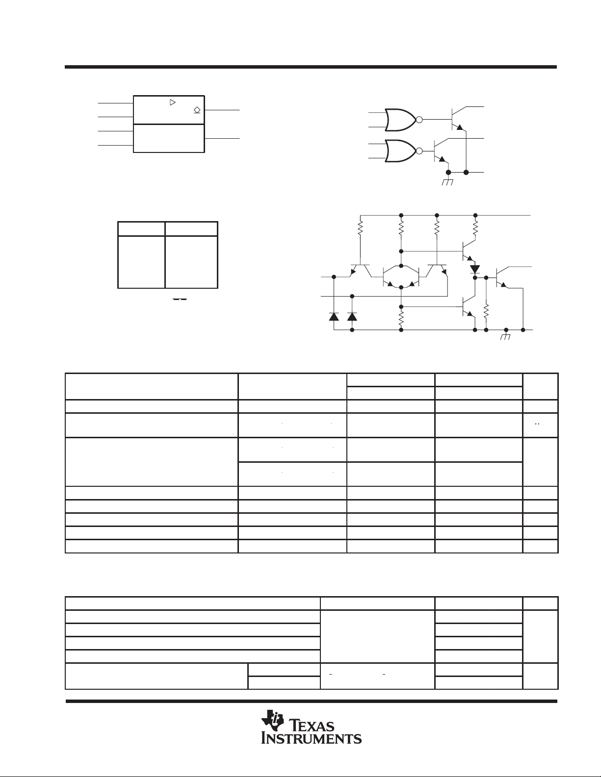
logic symbol
1
1A
2
1B
6
2A
7
2B
†
This symbol is in accordance with ANSI/IEEE Std 91-1984
and IEC Publication 617-12.
Pin numbers shown are for D, JG, and P packages.
†
&
FUNCTION TABLE
(each driver)
A
B
L L L (on state)
L H L (on state)
H L L (on state)
H H H (off state)
positive logic:
Y = AB or A
+ B
logic diagram (positive logic)
3
1Y
5
2Y
1A
1B
2A
2B
1
2
6
7
schematic (each driver)
Y
A
B
Resistor values shown are nominal.
4 kΩ 1.6 kΩ 130 Ω
500 Ω
1 kΩ
electrical characteristics over recommended operating free-air temperature range
SN55461 SN75461
MIN TYP‡MAX MIN TYP‡MAX
V
IK
I
I
I
IH
I
IL
I
CCH
I
CCL
†
For conditions shown as MIN or MAX, use the appropriate value specified under recommended operating conditions.
‡
All typical values are at VCC = 5 V, TA = 25°C.
Input clamp voltage VCC = MIN, II = –12 mA –1.2 –1.5 –1.2 –1.5 V
V
p
p
Input current at maximum input voltage VCC = MAX, VI = 5.5 V 1 1 mA
High-level input current VCC = MAX, VI = 2.4 V 40 40 µA
Low-level input current VCC = MAX, VI = 0.4 V –1 –1.6 –1 –1.6 mA
Supply current, outputs high VCC = MAX, VI = 5 V 8 11 8 11 mA
Supply current, outputs low VCC = MAX, VI = 0 56 76 56 76 mA
= MIN, V
VOH = 35 V
V
= MIN, V
IOL = 100 mA
V
= MIN, V
IOL = 300 mA
= MIN,
= 0.8 V,
= 0.8 V,
switching characteristics, VCC = 5 V, TA = 25°C
PARAMETER TEST CONDITIONS MIN TYP MAX UNIT
t
PLH
t
PHL
t
TLH
t
THL
Propagation delay time, low-to-high-level output 30 55
Propagation delay time, high-to-low-level output
Transition time, low-to-high-level output
Transition time, high-to-low-level output 10 20
p
SN55461
SN75461
I
≈ 200 mA, C
RL = 50 Ω,
VS = 30 V, IO ≈ 300 mA,
See Figure 2
= 15 pF,
See Figure 1
VS–10
VS–10
3
1Y
5
2Y
4
GND
25 40
8 20
V
CC
Y
GND
POST OFFICE BOX 655303 • DALLAS, TEXAS 75265
3
Page 4

SN55461 THRU SN55463
PARAMETER
TEST CONDITIONS
†
UNIT
IOHHigh-level output current
CC
,
IL
,
300
100µA
CC
,
IH
,
0.25
0.5
0.25
0.4
VOLLow-level output voltage
V
CC
,
IH
,
0.5
0.8
0.5
0.7
O
,
L
,
ns
VOHHigh-level output voltage after switching
S
O
mV
SN75461 THRU SN75463
DUAL PERIPHERAL DRIVERS
SLRS022A – DECEMBER 1976 – REVISED OCT OBER 1995
logic symbol
1A
1B
2A
2B
†
This symbol is in accordance with ANSI/IEEE Std 91-1984
and IEC Publication 617-12.
Pin numbers shown are for D, JG, and P packages.
†
1
2
6
7
FUNCTION TABLE
(each driver)
A
B
L L H (off state)
L H H (off state)
H L H (off state)
H H L (on state)
positive logic:
Y = AB
or A + B
logic diagram (positive logic)
&
3
1Y
5
2Y
1A
1B
2A
2B
1
2
6
7
schematic (each driver)
1 kΩ
1.6 kΩ
1.6 kΩ
1 kΩ
Y
A
B
Resistor values shown are nominal.
4 kΩ
electrical characteristics over recommended operating free-air temperature range
SN55462 SN75462
MIN TYP‡MAX MIN TYP‡MAX
V
Input clamp voltage VCC = MIN, II = –12 mA –1.2 –1.5 –1.2 –1.5 V
IK
V
p
p
I
Input current at maximum input voltage VCC = MAX, VI = 5.5 V 1 1 mA
I
I
High-level input current VCC = MAX, VI = 2.4 V 40 40 µA
IH
I
Low-level input current VCC = MAX, VI = 0.4 V –1.1 –1.6 –1.1 –1.6 mA
IL
I
Supply current, outputs high VCC = MAX, VI = 0 13 17 13 17 mA
CCH
I
Supply current, outputs low VCC = MAX, VI = 5 V 61 76 61 76 mA
CCL
†
For conditions shown as MIN or MAX, use the appropriate value specified under recommended operating conditions.
‡
All typical values are at VCC = 5 V, TA = 25°C.
= MIN, V
VOH = 35 V
V
= MIN, V
IOL = 100 mA
V
= MIN, V
IOL = 300 mA
= 0.8 V,
= MIN,
= MIN,
switching characteristics, VCC = 5 V, TA = 25°C
PARAMETER TEST CONDITIONS MIN TYP MAX UNIT
t
Propagation delay time, low-to-high-level output 45 65
PLH
t
Propagation delay time, high-to-low-level output
PHL
t
Transition time, low-to-high-level output
TLH
t
Transition time, high-to-low-level output 10 20
THL
p
SN55462
SN75462
I
≈ 200 mA, C
RL = 50 Ω,
VS = 30 V, IO ≈ 300 mA,
See Figure 2
= 15 pF,
See Figure 1
VS–10
VS–10
3
1Y
5
2Y
4
GND
130 Ω
500 Ω
30 50
13 25
V
CC
Y
GND
4
POST OFFICE BOX 655303 • DALLAS, TEXAS 75265
Page 5
SN55461 THRU SN55463
PARAMETER
TEST CONDITIONS
†
UNIT
IOHHigh-level output current
CC
,
IH
,
300
100µA
CC
,
IL
,
0.25
0.5
0.25
0.4
VOLLow-level output voltage
V
CC
,
IL
,
0.5
0.8
0.5
0.7
O
,
L
,
ns
VOHHigh-level output voltage after switching
S
O
mV
SN75461 THRU SN75463
DUAL PERIPHERAL DRIVERS
SLRS022A – DECEMBER 1976 – REVISED OCT OBER 1995
logic symbol
1A
1B
2A
2B
†
This symbol is in accordance with ANSI/IEEE Std 91-1984
and IEC Publication 617-12.
Pin numbers shown are for D, JG, and P packages.
†
1
2
6
7
FUNCTION TABLE
(each driver)
A
B
L L L (on state)
L H H (off state)
H L H (off state)
H H H (off state)
positive logic:
Y = A + B or A
≥1
3
1Y
5
2Y
Y
B
logic diagram (positive logic)
1
1A
2
1B
6
2A
7
2B
schematic (each driver)
4 kΩ 1.6 kΩ 130 Ω
A
B
1 kΩ
Resistor values shown are nominal.
4 kΩ
3
1Y
5
2Y
4
GND
V
CC
Y
500 Ω
GND
electrical characteristics over recommended operating free-air temperature range
SN55463 SN75463
TYP
‡
MAX MIN
TYP
MIN
V
Input clamp voltage VCC = MIN, II = –12 mA –1.2 –1.5 –1.2 –1.5 V
IK
V
p
p
I
Input current at maximum input voltage VCC = MAX, VI = 5.5 V 1 1 mA
I
I
High-level input current VCC = MAX, VI = 2.4 V 40 40 µA
IH
I
Low-level input current VCC = MAX, VI = 0.4 V –1 –1.6 –1 –1.6 mA
IL
I
Supply current, outputs high VCC = MAX, VI = 5 V 8 11 8 11 mA
CCH
I
Supply current, outputs low VCC = MAX, VI = 0 58 76 58 76 mA
CCL
†
For conditions shown as MIN or MAX, use the appropriate value specified under recommended operating conditions.
‡
All typical values are at VCC = 5 V, TA = 25°C.
= MIN, V
VOH = 35 V
V
= MIN, V
IOL = 100 mA
V
= MIN, V
IOL = 300 mA
= MIN,
= 0.8 V,
= 0.8 V,
switching characteristics, VCC = 5 V, TA = 25°C
PARAMETER TEST CONDITIONS MIN TYP MAX UNIT
t
Propagation delay time, low-to-high-level output 30 55
PLH
t
Propagation delay time, high-to-low-level output
PHL
t
Transition time, low-to-high-level output
TLH
t
Transition time, high-to-low-level output 10 25
THL
p
SN55463
SN75463
I
≈ 200 mA, C
RL = 50 Ω,
VS = 30 V, IO ≈ 300 mA,
See Figure 2
= 15 pF,
See Figure 1
VS–10
VS–10
‡
MAX
25 40
8 25
POST OFFICE BOX 655303 • DALLAS, TEXAS 75265
5
Page 6

SN55461 THRU SN55463
SN75461 THRU SN75463
DUAL PERIPHERAL DRIVERS
SLRS022A – DECEMBER 1976 – REVISED OCT OBER 1995
PARAMETER MEASUREMENT INFORMATION
≤ 5 ns
2.4 VInput
’461
’462
Pulse
Generator
(see Note A)
’463
0.4 V
TEST CIRCUIT
NOTES: A. The pulse generator has the following characteristics: PRR ≤ 1 MHz, ZO ≈ 50 Ω.
B. CL includes probe and jig capacitance.
RL = 50 Ω
Circuit
Under
Test
(see Note B)
GND
SUB
10 V
Output
CL = 15 pF
(see Note B)
Input
’461
’463
≤ 5 ns ≤ 10 ns
Input
’462
t
PHL
Output
t
THL
Figure 1. Test Circuit and Voltage Waveforms for Switching Times
Pulse
Generator
(see Note A)
2.4 VInput
’461
’462
’463
5 V
1N3064
Circuit
Under
Test
(see Note B)
GND
VS = 30 V
2 mH
65 Ω
Output
CL = 15 pF
(see Note B)
SUB
≤ 5 ns
Input
’461
’463
≤ 5 ns ≤ 10 ns
Input
’462
Output
10% 10%
0.5 µs
90% 90%
1.5 V1.5 V
50% 50%
10% 10%
VOLTAGE WAVEFORMS
1.5 V1.5 V
10% 10%
40 µs
90% 90%
1.5 V1.5 V
1.5 V1.5 V
90%90%
10%10%
≤ 10 ns
90%90%
10%10%
≤ 10 ns
t
PLH
90%90%
t
TLH
3 V
0 V
3 V
0 V
V
V
3 V
0 V
3 V
0 V
V
OH
OL
OH
0.4 V
TEST CIRCUIT
NOTES: A. The pulse generator has the following characteristics: PRR ≤ 12.5 kHz, ZO = 50 Ω.
B. CL includes probe and jig capacitance.
Figure 2. Test Circuit and Voltage Waveforms for Latch-Up Test
6
POST OFFICE BOX 655303 • DALLAS, TEXAS 75265
VOLTAGE WAVEFORMS
V
OL
Page 7

PACKAGE OPTION ADDENDUM
www.ti.com
17-Oct-2005
PACKAGING INFORMATION
Orderable Device Status
(1)
Package
Type
Package
Drawing
Pins Package
Qty
Eco Plan
JM38510/12908BPA ACTIVE CDIP JG 8 1 TBD A42 SNPB Level-NC-NC-NC
JM38510/12909BPA OBSOLETE CDIP JG 8 TBD Call TI Call TI
SN55461JG OBSOLETE CDIP JG 8 TBD Call TI Call TI
SN55462JG OBSOLETE CDIP JG 8 TBD Call TI Call TI
SN55463JG OBSOLETE CDIP JG 8 TBD Call TI Call TI
SN75461D OBSOLETE SOIC D 8 TBD Call TI Call TI
SN75461P OBSOLETE PDIP P 8 TBD Call TI Call TI
SN75462D ACTIVE SOIC D 8 75 Green (RoHS &
no Sb/Br)
SN75462DE4 ACTIVE SOIC D 8 75 Green (RoHS &
no Sb/Br)
SN75462DR ACTIVE SOIC D 8 2500 Green (RoHS &
no Sb/Br)
SN75462DRE4 ACTIVE SOIC D 8 2500 Green (RoHS &
no Sb/Br)
SN75462P ACTIVE PDIP P 8 50 Pb-Free
SN75462PE4 ACTIVE PDIP P 8 50 Pb-Free
SN75463D OBSOLETE SOIC D 8 TBD Call TI Call TI
SN75463DR OBSOLETE SOIC D 8 TBD Call TI Call TI
SN75463P ACTIVE PDIP P 8 50 Pb-Free
SN75463PE4 ACTIVE PDIP P 8 50 Pb-Free
SNJ55461FK OBSOLETE LCCC FK 20 TBD Call TI Call TI
SNJ55461JG OBSOLETE CDIP JG 8 TBD Call TI Call TI
SNJ55462FK ACTIVE LCCC FK 20 1 TBD POST-PLATE Level-NC-NC-NC
SNJ55462JG ACTIVE CDIP JG 8 1 TBD A42 SNPB Level-NC-NC-NC
SNJ55463JG OBSOLETE CDIP JG 8 TBD Call TI Call TI
(1)
The marketing status values are defined as follows:
ACTIVE: Product device recommended for new designs.
LIFEBUY: TI has announced that the device will be discontinued, and a lifetime-buy period is in effect.
NRND: Not recommended for new designs. Device is in production to support existing customers, but TI does not recommend using this part in
a new design.
PREVIEW: Device has been announced but is not in production. Samples may or may not be available.
OBSOLETE: TI has discontinued the production of the device.
(RoHS)
(RoHS)
(RoHS)
(RoHS)
(2)
Lead/Ball Finish MSL Peak Temp
CU NIPDAU Level-1-260C-UNLIM
CU NIPDAU Level-1-260C-UNLIM
CU NIPDAU Level-1-260C-UNLIM
CU NIPDAU Level-1-260C-UNLIM
CU NIPDAU Level-NC-NC-NC
CU NIPDAU Level-NC-NC-NC
CU NIPDAU Level-NC-NC-NC
CU NIPDAU Level-NC-NC-NC
(3)
(2)
Eco Plan - The planned eco-friendly classification: Pb-Free (RoHS) or Green (RoHS & no Sb/Br) - please check
http://www.ti.com/productcontent for the latest availability information and additional product content details.
TBD: The Pb-Free/Green conversion plan has not been defined.
Pb-Free (RoHS): TI's terms "Lead-Free" or "Pb-Free" mean semiconductor products that are compatible with the current RoHS requirements
for all 6 substances, including the requirement that lead not exceed 0.1% by weight in homogeneous materials. Where designed to be soldered
at high temperatures, TI Pb-Free products are suitable for use in specified lead-free processes.
Green (RoHS & no Sb/Br): TI defines "Green" to mean Pb-Free (RoHS compatible), and free of Bromine (Br) and Antimony (Sb) based flame
retardants (Br or Sb do not exceed 0.1% by weight in homogeneous material)
(3)
MSL, Peak Temp. -- The Moisture Sensitivity Level rating according to the JEDEC industry standard classifications, and peak solder
temperature.
Addendum-Page 1
Page 8

PACKAGE OPTION ADDENDUM
www.ti.com
Important Information and Disclaimer:The information provided on this page represents TI's knowledge and belief as of the date that it is
provided. TI bases its knowledge and belief on information provided by third parties, and makes no representation or warranty as to the
accuracy of such information. Efforts are underway to better integrate information from third parties. TI has taken and continues to take
reasonable steps to provide representative and accurate information but may not have conducted destructive testing or chemical analysis on
incoming materials and chemicals. TI and TI suppliers consider certain information to be proprietary, and thus CAS numbers and other limited
information may not be available for release.
In no event shall TI's liability arising out of such information exceed the total purchase price of the TI part(s) at issue in this document sold by TI
to Customer on an annual basis.
17-Oct-2005
Addendum-Page 2
Page 9

MECHANICAL DATA
MCER001A – JANUARY 1995 – REVISED JANUARY 1997
JG (R-GDIP-T8) CERAMIC DUAL-IN-LINE
0.400 (10,16)
0.355 (9,00)
0.063 (1,60)
0.015 (0,38)
0.100 (2,54)
8
1
5
4
0.065 (1,65)
0.045 (1,14)
0.020 (0,51) MIN
0.023 (0,58)
0.015 (0,38)
0.280 (7,11)
0.245 (6,22)
0.310 (7,87)
0.290 (7,37)
0.200 (5,08) MAX
Seating Plane
0.130 (3,30) MIN
0°–15°
0.014 (0,36)
0.008 (0,20)
NOTES: A. All linear dimensions are in inches (millimeters).
B. This drawing is subject to change without notice.
C. This package can be hermetically sealed with a ceramic lid using glass frit.
D. Index point is provided on cap for terminal identification.
E. Falls within MIL STD 1835 GDIP1-T8
4040107/C 08/96
POST OFFICE BOX 655303 • DALLAS, TEXAS 75265
Page 10

MECHANICAL DATA
MLCC006B – OCTOBER 1996
FK (S-CQCC-N**) LEADLESS CERAMIC CHIP CARRIER
28 TERMINAL SHOWN
A SQ
B SQ
20
22
23
24
25
19
21
12826 27
12
1314151618 17
0.020 (0,51)
0.010 (0,25)
MIN
0.342
(8,69)
0.442
0.640
0.739
0.938
1.141
A
0.358
(9,09)
0.458
(11,63)
0.660
(16,76)
0.761
(19,32)(18,78)
0.962
(24,43)
1.165
(29,59)
NO. OF
TERMINALS
**
11
10
9
8
7
6
5
432
20
28
44
52
68
84
0.020 (0,51)
0.010 (0,25)
(11,23)
(16,26)
(23,83)
(28,99)
MINMAX
0.307
(7,80)
0.406
(10,31)
0.495
(12,58)
0.495
(12,58)
0.850
(21,6)
1.047
(26,6)
0.080 (2,03)
0.064 (1,63)
B
MAX
0.358
(9,09)
0.458
(11,63)
0.560
(14,22)
0.560
(14,22)
0.858
(21,8)
1.063
(27,0)
0.055 (1,40)
0.045 (1,14)
0.028 (0,71)
0.022 (0,54)
0.050 (1,27)
NOTES: A. All linear dimensions are in inches (millimeters).
B. This drawing is subject to change without notice.
C. This package can be hermetically sealed with a metal lid.
D. The terminals are gold plated.
E. Falls within JEDEC MS-004
POST OFFICE BOX 655303 • DALLAS, TEXAS 75265
0.045 (1,14)
0.035 (0,89)
0.045 (1,14)
0.035 (0,89)
4040140/D 10/96
Page 11

MECHANICAL DATA
MPDI001A – JANUARY 1995 – REVISED JUNE 1999
P (R-PDIP-T8) PLASTIC DUAL-IN-LINE
0.400 (10,60)
0.355 (9,02)
8
5
0.260 (6,60)
0.240 (6,10)
1
0.021 (0,53)
0.015 (0,38)
NOTES: A. All linear dimensions are in inches (millimeters).
B. This drawing is subject to change without notice.
C. Falls within JEDEC MS-001
4
0.070 (1,78) MAX
0.020 (0,51) MIN
0.200 (5,08) MAX
0.125 (3,18) MIN
0.100 (2,54)
0.010 (0,25)
Seating Plane
M
0.325 (8,26)
0.300 (7,62)
0.015 (0,38)
Gage Plane
0.010 (0,25) NOM
0.430 (10,92)
MAX
4040082/D 05/98
For the latest package information, go to http://www.ti.com/sc/docs/package/pkg_info.htm
POST OFFICE BOX 655303 • DALLAS, TEXAS 75265
Page 12

Page 13

IMPORTANT NOTICE
Texas Instruments Incorporated and its subsidiaries (TI) reserve the right to make corrections, modifications,
enhancements, improvements, and other changes to its products and services at any time and to discontinue
any product or service without notice. Customers should obtain the latest relevant information before placing
orders and should verify that such information is current and complete. All products are sold subject to TI’s terms
and conditions of sale supplied at the time of order acknowledgment.
TI warrants performance of its hardware products to the specifications applicable at the time of sale in
accordance with TI’s standard warranty. Testing and other quality control techniques are used to the extent TI
deems necessary to support this warranty . Except where mandated by government requirements, testing of all
parameters of each product is not necessarily performed.
TI assumes no liability for applications assistance or customer product design. Customers are responsible for
their products and applications using TI components. To minimize the risks associated with customer products
and applications, customers should provide adequate design and operating safeguards.
TI does not warrant or represent that any license, either express or implied, is granted under any TI patent right,
copyright, mask work right, or other TI intellectual property right relating to any combination, machine, or process
in which TI products or services are used. Information published by TI regarding third-party products or services
does not constitute a license from TI to use such products or services or a warranty or endorsement thereof.
Use of such information may require a license from a third party under the patents or other intellectual property
of the third party, or a license from TI under the patents or other intellectual property of TI.
Reproduction of information in TI data books or data sheets is permissible only if reproduction is without
alteration and is accompanied by all associated warranties, conditions, limitations, and notices. Reproduction
of this information with alteration is an unfair and deceptive business practice. TI is not responsible or liable for
such altered documentation.
Resale of TI products or services with statements different from or beyond the parameters stated by TI for that
product or service voids all express and any implied warranties for the associated TI product or service and
is an unfair and deceptive business practice. TI is not responsible or liable for any such statements.
Following are URLs where you can obtain information on other Texas Instruments products and application
solutions:
Products Applications
Amplifiers amplifier.ti.com Audio www.ti.com/audio
Data Converters dataconverter.ti.com Automotive www.ti.com/automotive
DSP dsp.ti.com Broadband www.ti.com/broadband
Interface interface.ti.com Digital Control www.ti.com/digitalcontrol
Logic logic.ti.com Military www.ti.com/military
Power Mgmt power.ti.com Optical Networking www.ti.com/opticalnetwork
Microcontrollers microcontroller.ti.com Security www.ti.com/security
Telephony www.ti.com/telephony
Video & Imaging www.ti.com/video
Wireless www.ti.com/wireless
Mailing Address: Texas Instruments
Post Office Box 655303 Dallas, Texas 75265
Copyright 2005, Texas Instruments Incorporated
 Loading...