

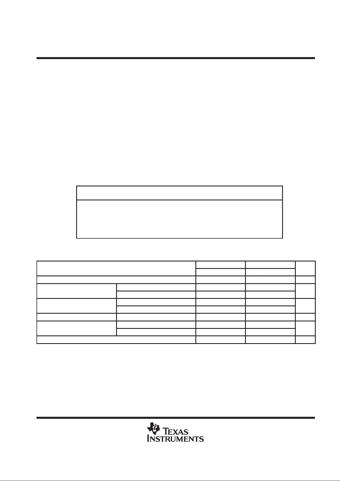
Texas Instruments SN55138J, SN75138D, SN75138N, SN75138NS, SNJ55138FK Datasheet
...
SN55138, SN75138
QUADRUPLE BUS TRANSCEIVERS
SLLS079B – SEPTEMBER 1973 – REVISED MA Y 1995
1
POST OFFICE BOX 655303 • DALLAS, TEXAS 75265
D
Single 5-V Supply
D
High-Input-Impedance, High-Threshold
Receivers
D
Common Driver Strobe
D
TTL-Compatible Driver and Strobe Inputs
With Clamp Diodes
D
High-Speed Operation
D
100-mA Open-Collector Driver Outputs
D
Four Independent Channels
D
TTL-Compatible Receiver Output
description
The SN55138 and SN75138 quadruple bus
transceivers are designed for two-way data
communication over single-ended transmission
lines. Each of the four identical channels consists
of a driver with TTL inputs and a receiver with a
TTL output. The driver open-collector output is
designed to handle loads up to 100-mA open
collector. The receiver input is internally
connected to the driver output, and has a high
impedance to minimize loading of the
transmission line. Because of the high driveroutput current and the high receiver-input
impedance, a very large number (typically
hundreds) of transceivers may be connected to a
single data bus.
The receiver design also features a threshold of 2.3 V (typical), providing a wider noise margin than would be
possible with a receiver having the usual TTL threshold. A strobe turns off all drivers (high impedance) but does
not affect receiver operation. These circuits are designed for operation from a single 5-V supply and include a
provision to minimize loading of the data bus when the power-supply voltage is zero.
The SN55138 is characterized for operation over the full military temperature range of –55°C to 125°C. The
SN75138 is characterized for operation from 0°C to 70°C.
Copyright 1995, Texas Instruments Incorporated
PRODUCTION DATA information is current as of publication date.
Products conform to specifications per the terms of Texas Instruments
standard warranty. Production processing does not necessarily include
testing of all parameters.
Please be aware that an important notice concerning availability, standard warranty, and use in critical applications of
Texas Instruments semiconductor products and disclaimers thereto appears at the end of this data sheet.
3 2 1 20 19
910111213
4
5
6
7
8
18
17
16
15
14
4R
4D
NC
S
3D
1R
1D
NC
2D
2R
SN55138 . . . FK PACKAGE
(TOP VIEW)
1B
GND
NC
3B
3R
4B
2B
GND
NC
NC – No internal connection
1
2
3
4
5
6
7
8
16
15
14
13
12
11
10
9
GND
1B
1R
1D
2D
2R
2B
GND
V
CC
4B
4R
4D
S
3D
3R
3B
SN55138 ...J OR W PACKAGE
SN75138 ...D OR N PACKAGE
(TOP VIEW)
CC
V

SN55138, SN75138
QUADRUPLE BUS TRANSCEIVERS
SLLS079B – SEPTEMBER 1973 – REVISED MA Y 1995
2
POST OFFICE BOX 655303 • DALLAS, TEXAS 75265
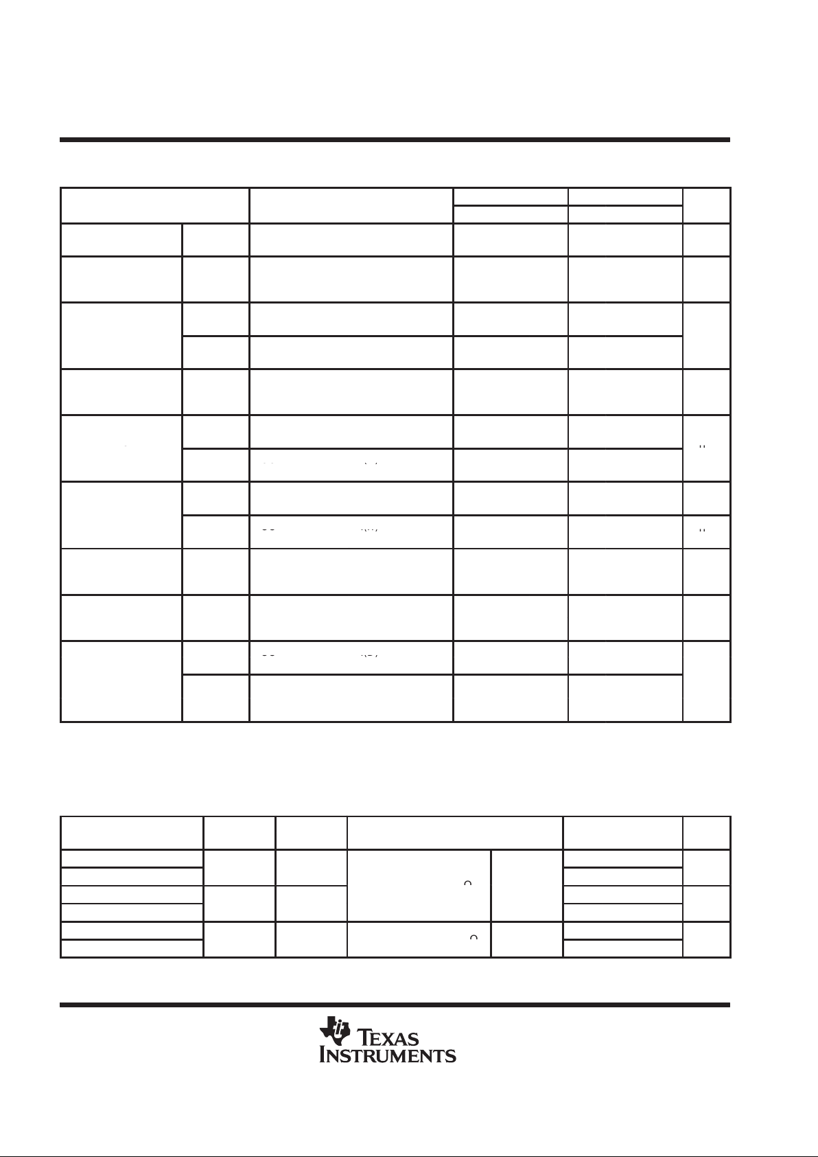
Function Tables
TRANSMITTING
INPUTS
OUTPUTS
S D B R
L H L H
L L H L
RECEIVING
INPUTS
OUTPUT
S B D
R
H H X L
H L X H
H = high level, L = low level, X = irrelevant
logic symbol
†
12
4
3
5
6
11
10
13
14
4B
3B
2B
1B
4R
4D
3R
3D
2R
2D
1R
1D
S
15
9
7
2
EN2
1
2
†
This symbol is in accordance with ANSI/IEEE Std 91-1984
and IEC Publication 617-12.
Pin numbers shown are for D, J, N, and W packages.
logic diagram (positive logic)
3
14
13
10
11
6
5
4
12
4B
3B
2B
1B
4R
4D
3R
3D
2R
2D
1R
1D
S
15
9
7
2
schematics of inputs and outputs
Output
130 Ω NOM
V
CC
TYPICAL OF ALL
RECEIVER OUTPUTSDRIVER OUTPUTS
TYPICAL OF ALL
Output
EQUIVALENT OF
EACH RECEIVER INPUT
2 kΩ NOM
V
CC
Input
4 kΩ NOM
Input
V
CC
STROBE AND DRIVER INPUT
EQUIVALENT OF EACH
SN55138, SN75138
QUADRUPLE BUS TRANSCEIVERS
SLLS079B – SEPTEMBER 1973 – REVISED MA Y 1995
3
POST OFFICE BOX 655303 • DALLAS, TEXAS 75265
absolute maximum ratings over operating free-air temperature (unless otherwise noted)
†
Supply voltage, V
CC
(see Note 1) 7 V. . . . . . . . . . . . . . . . . . . . . . . . . . . . . . . . . . . . . . . . . . . . . . . . . . . . . . . . . . . . .
Input voltage, V
I
5.5 V. . . . . . . . . . . . . . . . . . . . . . . . . . . . . . . . . . . . . . . . . . . . . . . . . . . . . . . . . . . . . . . . . . . . . . . . . .
Driver off-state output voltage 7 V. . . . . . . . . . . . . . . . . . . . . . . . . . . . . . . . . . . . . . . . . . . . . . . . . . . . . . . . . . . . . . . .
Low-level output current into the driver output 150 mA. . . . . . . . . . . . . . . . . . . . . . . . . . . . . . . . . . . . . . . . . . . . . .
Continuous total dissipation See Dissipation Rating Table. . . . . . . . . . . . . . . . . . . . . . . . . . . . . . . . . . . . . . . . . . .
Operating free-air temperature range, T
A
: SN55138 –55°C to 125°C. . . . . . . . . . . . . . . . . . . . . . . . . . . . . . . . .
SN75138 0°C to 70°C. . . . . . . . . . . . . . . . . . . . . . . . . . . . . . . . . . . .
Storage temperature range, T
stg
–65°C to 150°C. . . . . . . . . . . . . . . . . . . . . . . . . . . . . . . . . . . . . . . . . . . . . . . . . . .
Lead temperature 1,6 mm (1/16 inch) from case for 10 seconds: D, N, or W package 260°C. . . . . . . . . . . . .
Case temperature for 60 seconds, T
C
: FK package 260°C. . . . . . . . . . . . . . . . . . . . . . . . . . . . . . . . . . . . . . . . . .
Lead temperature 1,6 mm (1/16 inch) from case for 60 seconds: J package 300°C. . . . . . . . . . . . . . . . . . . . .
†
Stresses beyond those listed under “absolute maximum ratings” may cause permanent damage to the device. These are stress ratings only, and
functional operation of the device at these or any other conditions beyond those indicated under “recommended operating conditions” is not
implied. Exposure to absolute-maximum-rated conditions for extended periods may affect device reliability.
NOTE 1: All voltage values are with respect to both ground terminals connected together.
DISSIPATION RATING TABLE
T
≤ 25°C DERATING FACTOR T
= 70°C T
= 125°C
PACKAGE
A
POWER RATING ABOVE TA = 25°CAPOWER RATINGAPOWER RATING
D 950 mW 7.6 mW/°C 608 mW —
FK
‡
1375 mW 11.0 mW/°C 880 mW 275 mW
J
‡
1375 mW 11.0 mW/°C 880 mW 275 mW
N 1150 mW 9.2 mW/°C 736 mW —
W 1000 mW 8.0 mW/°C 640 mW 200 mW
‡
In the FK and J packages, the SN55138 chip is alloy mounted.
recommended operating conditions
SN55138 SN75138
MIN NOM MAX MIN NOM MAX
UNIT
Supply voltage, V
CC
4.5 5.5 4.75 5 5.25 V
p
Driver or strobe 2 2
High-level input voltage, V
IH
Receiver 3.2 2.9
V
p
Driver or strobe 0.8 0.8
Low-level input voltage, V
IL
Receiver 1.5 1.8
V
High-level output current, I
OH
Receiver output –400 –400 µA
p
Driver output 100 100
Low-level output current, I
OL
Receiver output 16 16
mA
Operating free-air temperature, T
A
–55 125 0 70 °C
SN55138, SN75138
QUADRUPLE BUS TRANSCEIVERS
SLLS079B – SEPTEMBER 1973 – REVISED MA Y 1995
4
POST OFFICE BOX 655303 • DALLAS, TEXAS 75265
electrical characteristics over recommended operating free-air temperature range (unless
otherwise noted)
SN55138 SN75138
PARAMETER
TEST CONDITIONS
†
MIN TYP‡MAX MIN TYP‡MAX
UNIT
V
IK
Input clamp
voltage
Driver or
strobe
VCC = MIN, II = –12 mA –1.5 –1.5 V
V
OH
High-level
output
voltage
Receiver
VCC = MIN,
V
IL(R)
= VIL max,
V
IH(S)
= 2 V,
IOH = –400 µA
2.4 3.5 2.4 3.5 V
Low-level
p
Driver
VCC = MIN,
V
IL(S)
= 0.8 V,
V
IH(D)
= 2 V,
IOL = 100 mA
0.45 0.45
V
OL
out ut
voltage
Receiver
VCC = MIN,
V
IH(S)
= 2 V,
V
IH(R)
= VIH min,
IOL = 16 mA
0.4 0.4
V
II(max)
Input current
at maximum
input voltage
Driver or
strobe
VCC = MAX, VI = V
CC
1 1 mA
High-level
Driver or
strobe
VCC = MAX, VI = 2.4 V 40 40
I
IH
g
input current
VCC = 5 V, V
I
(R)
= 4.5 V,
µ
A
Receiver
CC
V
I(S)
= 2 V
I(R)
25
30025300
Low-level
Driver or
strobe
VCC = MAX, VI = 0.4 V –1 –1.6 –1 –1.6 mA
I
IL
input current
VCC = MAX, V
I(R
)
= 0.45 V ,
Receiver
CC
V
I(S)
= 2 V
I(R)
–
50–50µA
Input current
p
I
I(off)
with ower
off
Receiver
V
CC
=
0
,
V
I
=
4.5 V
1.1
1.5
1.1
1.5
mA
Short-circuit
p
I
OS
out ut
current
§
Receiver
V
CC
=
MAX
–
20–55–18–55
mA
All driver VCC = MAX, V
I(D
)
= 2 V,
pp
outputs lowCCV
I(S)
= 0.8 V
I(D)
506550
65
I
CC
Suppl
y
current
All driver
p
VCC = MAX, V
I(R)
= 3.5 V,
mA
out uts
high
V
I(S)
= 2 V,
Receiver outputs open
425542
55
†
For conditions shown as MIN or MAX, use the appropriate value specified under recommended operating conditions. Parenthetical letters D,
R, and S used with VI refer to the driver input, receiver input, and strobe input, respectively.
‡
All typical values are at VCC = 5 V, TA = 25°C.
§
Not more than one output should be shorted at a time.
switching characteristics, VCC = 5 V, TA = 25°C
FROM TO
PARAMETER
¶
(INPUT) (OUTPUT)
TEST CONDITIONS
MIN
TYP
MAX
UNIT
t
PLH
15 24
t
PHL
Driver
Driver
p
14 24
ns
t
PLH
C
L
= 50 pF,
R
L
= 50 Ω,
See Figure 1
18 28
t
PHL
Strobe
Driver
22 32
ns
t
PLH
p
7 15
t
PHL
Receiver
Receiver
C
L
= 15
pF
R
L
=
400 Ω
,
See Figure 2
8 15
ns
¶
t
PLH
= propagation delay time, low- to high-level output
t
PHL
= propagation delay time, high- to low-level output
 Loading...