

Datasheet SN54LS373, SN54LS374, SN54S373, SN54S374, SN74LS373 Datasheet (TEXAS INSTRUMENTS)
...Page 1
SN54LS373, SN54LS374, SN54S373, SN54S374,
SN74LS373, SN74LS374, SN74S373, SN74S374
OCTAL D-TYPE TRANSPARENT LATCHES AND EDGE-TRIGGERED FLIP-FLOPS
SDLS165B – OCTOBER 1975 – REVISED AUGUST 2002
D
Choice of Eight Latches or Eight D-Type
Flip-Flops in a Single Package
D
3-State Bus-Driving Outputs
D
Full Parallel Access for Loading
D
Buffered Control Inputs
D
Clock-Enable Input Has Hysteresis to
Improve Noise Rejection (’S373 and ’S374)
D
P-N-P Inputs Reduce DC Loading on Data
Lines (’S373 and ’S374)
description
These 8-bit registers feature 3-state outputs
designed specifically for driving highly capacitive
or relatively low-impedance loads. The
high-impedance 3-state and increased
high-logic-level drive provide these registers with
the capability of being connected directly to and
driving the bus lines in a bus-organized system
without need for interface or pullup components.
These devices are particularly attractive for
implementing buffer registers, I/O ports,
bidirectional bus drivers, and working registers.
The eight latches of the ’LS373 and ’S373 are
transparent D-type latches, meaning that while
the enable (C or CLK) input is high, the Q outputs
follow the data (D) inputs. When C or CLK is taken
low, the output is latched at the level of the data
that was set up.
The eight flip-flops of the ’LS374 and ’S374 are
edge-triggered D-type flip-flops. On the positive
transition of the clock, the Q outputs are set to the
logic states that were set up at the D inputs.
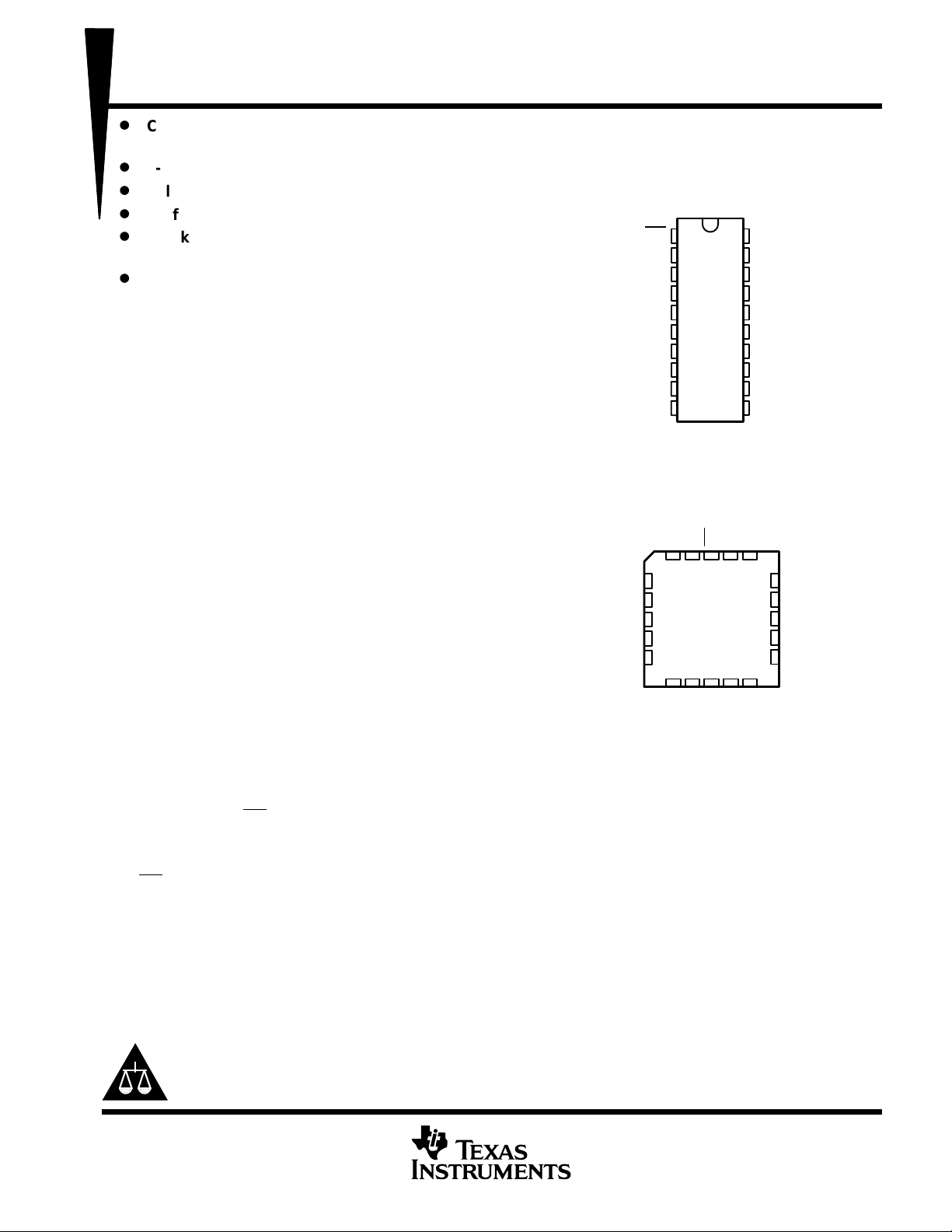
SN54LS373, SN54LS374, SN54S373,
SN74LS373, SN74S374 . . . DW, N, OR NS PACKAGE
SN54S374 . . . J OR W PACKAGE
SN74LS374 . . . DB, DW, N, OR NS PACKAGE
SN74S373 . . . DW OR N PACKAGE
†
C for ’LS373 and ’S373; CLK for ’LS374 and ’S374.
SN54LS373, SN54LS374, SN54S373,
SN54S374 . . . FK PACKAGE
2D
2Q
3Q
3D
4D
†
C for ’LS373 and ’S373; CLK for ’LS374 and ’S374.
(TOP VIEW)
1
OC
2
1Q
3
1D
4
2D
5
2Q
6
3Q
7
3D
8
4D
9
4Q
GND
10
(TOP VIEW)
1D1QOC
3212019
4
5
6
7
8
910111213
4Q
†
GND
20
V
CC
19
8Q
18
8D
17
7D
16
7Q
15
6Q
14
6D
13
5D
12
5Q
†
11
C
CC
8Q
V
8D
18
7D
17
7Q
16
6Q
15
6D
14
5D
C
5Q
Schmitt-trigger buffered inputs at the enable/clock lines of the ’S373 and ’S374 devices simplify system design
as ac and dc noise rejection is improved by typically 400 mV due to the input hysteresis. A buffered
output-control (OC
) input can be used to place the eight outputs in either a normal logic state (high or low logic
levels) or the high-impedance state. In the high-impedance state, the outputs neither load nor drive the bus lines
significantly.
OC
does not affect the internal operation of the latches or flip-flops. That is, the old data can be retained or new
data can be entered, even while the outputs are off.
Please be aware that an important notice concerning availability, standard warranty, and use in critical applications of
Texas Instruments semiconductor products and disclaimers thereto appears at the end of this data sheet.
PRODUCTION DATA information is current as of publication date.
Products conform to specifications per the terms of Texas Instruments
standard warranty. Production processing does not necessarily include
testing of all parameters.
POST OFFICE BOX 655303 • DALLAS, TEXAS 75265
Copyright 2002, Texas Instruments Incorporated
On products compliant to MIL-PRF-38535, all parameters are tested
unless otherwise noted. On all other products, production
processing does not necessarily include testing of all parameters.
1
Page 2
SN54LS373, SN54LS374, SN54S373, SN54S374,
PDIP
N
LS373
LS374
0°C to 70°C
SOIC
DW
S373
S374
CDIP
J
LCCC
FK
SN74LS373, SN74LS374, SN74S373, SN74S374
OCTAL D-TYPE TRANSPARENT LATCHES AND EDGE-TRIGGERED FLIP-FLOPS
SDLS165B – OCTOBER 1975 – REVISED AUGUST 2002
ORDERING INFORMATION
T
A
°
°
SOP – NS
SSOP – DB Tape and reel SN74LS374DBR LS374A
–55°C to 125°C
CFP – W
†
Package drawings, standard packing quantities, thermal data, symbolization, and PCB design
guidelines are available at www.ti.com/sc/package.
PACKAGE
–
–
–
–
†
Tube SN74LS373N SN74LS373N
Tube SN74LS374N SN74LS374N
Tube SN74S373N SN74S373N
Tube SN74S374N SN74S374N
Tube SN74LS373DW
Tape and reel SN74LS373DWR
Tube SN74LS374DW
Tape and reel SN74LS374DWR
Tube SN74S373DW
Tape and reel SN74S373DWR
Tube SN74S374DW
Tape and reel SN74S374DWR
Tape and reel SN74LS373NSR 74LS373
Tape and reel SN74LS374NSR 74LS374
Tape and reel SN74S374NSR 74S374
Tube SN54LS373J SN54LS373J
Tube SNJ54LS373J SNJ54LS373J
Tube SN54LS374J SN54LS374J
Tube SNJ54LS374J SNJ54LS374J
Tube SN54S373J SN54S373J
Tube SNJ54S373J SNJ54S373J
Tube SN54S374J SN54S374J
Tube SNJ54S374J SNJ54S374J
Tube SNJ54LS373W SNJ54LS373W
Tube SNJ54LS374W SNJ54LS374W
Tube SNJ54S374W SNJ54S374W
Tube SNJ54LS373FK SNJ54LS373FK
Tube SNJ54LS374FK SNJ54LS374FK
Tube SNJ54S373FK SNJ54S373FK
Tube SNJ54S374FK SNJ54S374FK
ORDERABLE
PART NUMBER
TOP-SIDE
MARKING
2
POST OFFICE BOX 655303 • DALLAS, TEXAS 75265
Page 3
SN54LS373, SN54LS374, SN54S373, SN54S374,
SN74LS373, SN74LS374, SN74S373, SN74S374
OCTAL D-TYPE TRANSPARENT LATCHES AND EDGE-TRIGGERED FLIP-FLOPS
SDLS165B – OCTOBER 1975 – REVISED AUGUST 2002
Function Tables
’LS373, ’S373
(each latch)
INPUTS
OC C D
L H H H
L HL L
L LX Q
H X X Z
’LS374, ’S374
(each latch)
INPUTS
OC CLK D
L ↑ H H
L ↑ LL
L LX Q
H X X Z
OUTPUT
Q
0
OUTPUT
Q
0
POST OFFICE BOX 655303 • DALLAS, TEXAS 75265
3
Page 4
SN54LS373, SN54LS374, SN54S373, SN54S374,
SN74LS373, SN74LS374, SN74S373, SN74S374
OCTAL D-TYPE TRANSPARENT LATCHES AND EDGE-TRIGGERED FLIP-FLOPS
SDLS165B – OCTOBER 1975 – REVISED AUGUST 2002
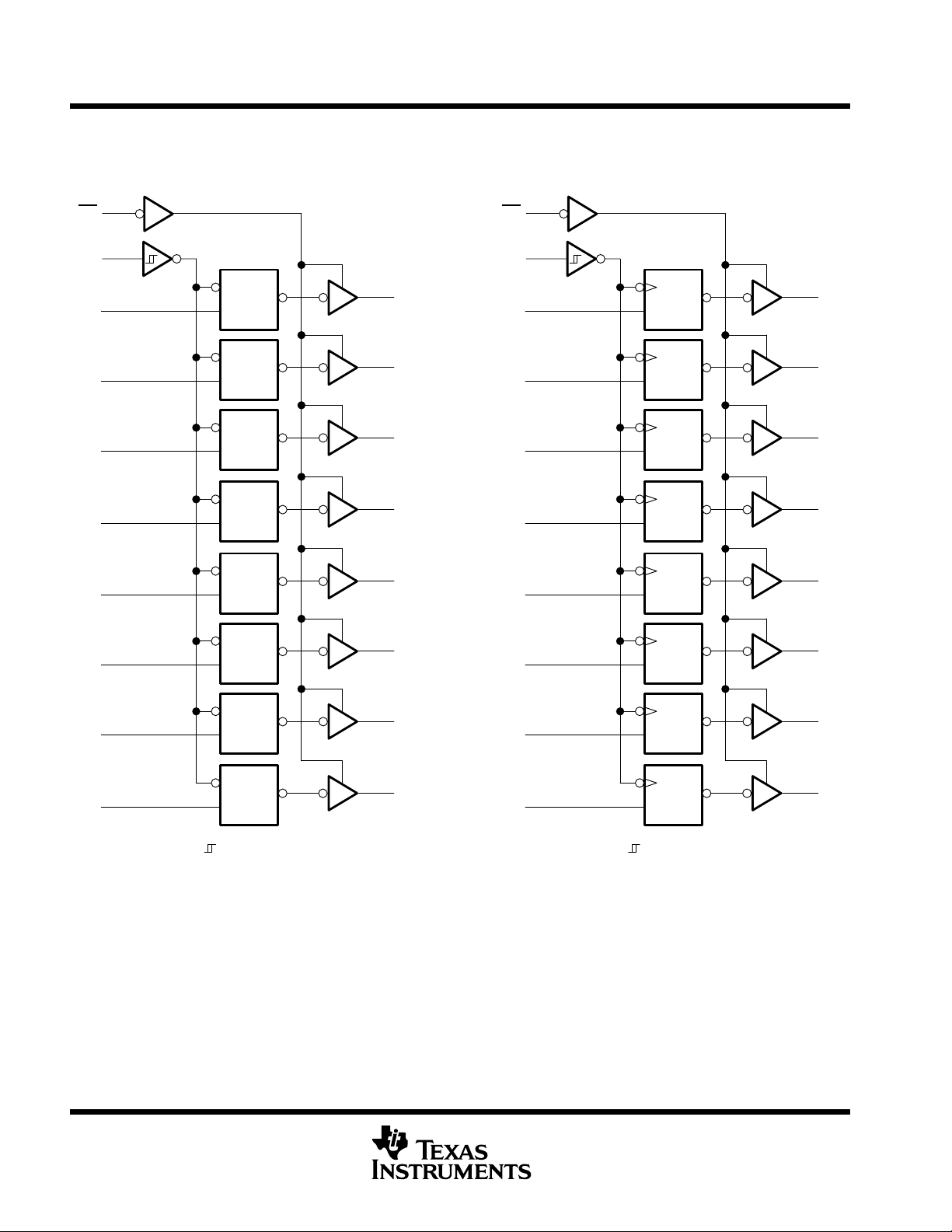
logic diagrams (positive logic)
OC
1D
2D
3D
4D
5D
’LS373, ’S373
Transparent Latches
1
11
C
3
4
7
8
13
C1
1D
C1
1D
C1
1D
C1
1D
C1
1D
12
2
1Q
5
2Q
6
3Q
9
4Q
5Q
OC
CLK
1D
2D
3D
4D
5D
Positive-Edge-Triggered Flip-Flops
1
11
3
4
7
8
13
’LS374, ’S374
C1
1D
C1
1D
C1
1D
C1
1D
C1
1D
12
2
1Q
5
2Q
6
3Q
9
4Q
5Q
14
6D
17
7D
18
8D
Pin numbers shown are for DB, DW, J, N, NS, and W packages.
C1
1D
C1
1D
C1
1D
for ’S373 Only
15
16
19
6Q
7Q
8Q
6D
7D
8D
14
17
18
C1
1D
C1
1D
C1
1D
for ’S374 Only
15
16
19
6Q
7Q
8Q
4
POST OFFICE BOX 655303 • DALLAS, TEXAS 75265
Page 5
SN54LS373, SN54LS374, SN54S373, SN54S374,
SN74LS373, SN74LS374, SN74S373, SN74S374
OCTAL D-TYPE TRANSPARENT LATCHES AND EDGE-TRIGGERED FLIP-FLOPS
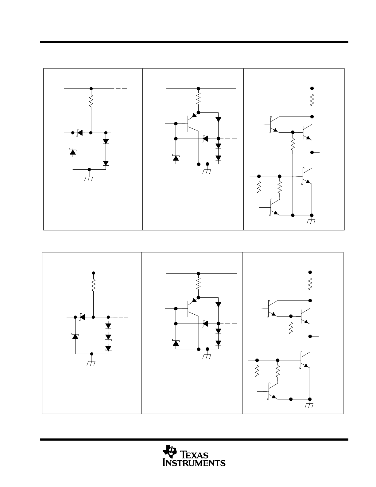
schematic of inputs and outputs
’LS373
EQUIVALENT OF DATA INPUTS EQUIVALENT OF ENABLE- AND
V
CC
Req = 20 kΩ NOM
Input
OUTPUT-CONTROL INPUTS
V
CC
Input
17 kΩ NOM
SDLS165B – OCTOBER 1975 – REVISED AUGUST 2002
TYPICAL OF ALL OUTPUTS
V
CC
100 Ω NOM
Output
EQUIVALENT OF DATA INPUTS
V
CC
30 kΩ NOM
Input
’LS374
EQUIVALENT OF CLOCK- AND
OUTPUT-CONTROL INPUTS
V
CC
17 kΩ NOM
Input
TYPICAL OF ALL OUTPUTS
100 Ω NOM
V
CC
Output
POST OFFICE BOX 655303 • DALLAS, TEXAS 75265
5
Page 6
SN54LS373, SN54LS374, SN54S373, SN54S374,
UNIT
twPulse duration
ns
tsuData setup time
ns
thData hold time
ns
SN74LS373, SN74LS374, SN74S373, SN74S374
OCTAL D-TYPE TRANSPARENT LATCHES AND EDGE-TRIGGERED FLIP-FLOPS
SDLS165B – OCTOBER 1975 – REVISED AUGUST 2002
absolute maximum ratings over operating free-air temperature range (unless otherwise noted)
(’LS devices)
Supply voltage, VCC (see Note 1) 7 V. . . . . . . . . . . . . . . . . . . . . . . . . . . . . . . . . . . . . . . . . . . . . . . . . . . . . . . . . . . . .
Input voltage, V
7 V. . . . . . . . . . . . . . . . . . . . . . . . . . . . . . . . . . . . . . . . . . . . . . . . . . . . . . . . . . . . . . . . . . . . . . . . . . . .
I
Off-state output voltage 5.5 V. . . . . . . . . . . . . . . . . . . . . . . . . . . . . . . . . . . . . . . . . . . . . . . . . . . . . . . . . . . . . . . . . . . .
Package thermal impedance, θ
(see Note 2): DB package 70°C/W. . . . . . . . . . . . . . . . . . . . . . . . . . . . . . . . .
JA
DW package 58°C/W. . . . . . . . . . . . . . . . . . . . . . . . . . . . . . . . .
N package 69°C/W. . . . . . . . . . . . . . . . . . . . . . . . . . . . . . . . . . .
NS package 60°C/W. . . . . . . . . . . . . . . . . . . . . . . . . . . . . . . . .
Storage temperature range, T
†
Stresses beyond those listed under “absolute maximum ratings” may cause permanent damage to the device. These are stress ratings only, and
functional operation of the device at these or any other conditions beyond those indicated under “recommended operating conditions” is not
implied. Exposure to absolute-maximum-rated conditions for extended periods may affect device reliability.
NOTES: 1. V oltage values are with respect to network ground terminal.
2. The package thermal impedance is calculated in accordance with JESD 51-7.
–65°C to 150°C. . . . . . . . . . . . . . . . . . . . . . . . . . . . . . . . . . . . . . . . . . . . . . . . . . .
stg
recommended operating conditions
SN54LS’ SN74LS’
MIN NOM MAX MIN NOM MAX
V
V
I
OH
I
OL
T
‡
The th specification applies only for data frequency below 10 MHz. Designs above 10 MHz should use a minimum of 5 ns (commercial only).
Supply voltage 4.5 5 5 4.75 5 5.25 V
CC
High-level output voltage 5.5 5.5 V
OH
High-level output current –1 –2.6 mA
Low-level output current 12 24 mA
CLK high 15 15
CLK low 15 15
p
Operating free-air temperature –55 125 0 70 °C
A
’LS373 5↓ 5↓
’LS374 20↑ 20↑
’LS373 20↓ 20↓
‡
’LS374
5↑ 0↑
†
6
POST OFFICE BOX 655303 • DALLAS, TEXAS 75265
Page 7
PARAMETER
TEST CONDITIONS
†
UNIT
VOHHigh-level output voltage
CC
,
IH
,
2.4
3.4
2.4
3.1
V
VOLLow-level output voltage
CC
,
IH
,
V
I
,
CC
,
IH
,
20
20mA
I
,
CC
,
IH
,
20–20mA
I
V
MAX
V
7 V
0.1
0.1
mA
ICCSupply current
CC
,
mA
PARAMETER
TEST CONDITIONS
UNIT
Data
Any Q
L
,
L
,
ns
C or CLK
Any Q
L
,
L
,
ns
OC
Any Q
L
,
L
,
ns
t
152515
28
OC
Any Q
R
667 Ω
C
5 pF
ns
t
122012
20
SN54LS373, SN54LS374, SN54S373, SN54S374,
SN74LS373, SN74LS374, SN74S373, SN74S374
OCTAL D-TYPE TRANSPARENT LATCHES AND EDGE-TRIGGERED FLIP-FLOPS
SDLS165B – OCTOBER 1975 – REVISED AUGUST 2002
electrical characteristics over recommended operating free-air temperature range (unless
otherwise noted)
SN54LS’ SN74LS’
MIN TYP‡MAX MIN TYP‡MAX
V
High-level input voltage 2 2 V
IH
V
Low-level input voltage 0.7 0.8 V
IL
V
Input clamp voltage VCC = MIN, II = –18 mA –1.5 –1.5 V
IK
V
p
p
Off-state output current, V
OZH
high-level voltage applied
Off-state output current, V
OZL
low-level voltage applied
Input current at maximum
I
input voltage
I
High-level input current VCC = MAX, VI = 2.7 V 20 20
IH
I
Low-level input current VCC = MAX, VI = 0.4 V –0.4 –0.4 mA
IL
I
Short-circuit output current§VCC = MAX –30 –130 –30 –130 mA
OS
pp
†
For conditions shown as MIN or MAX, use the appropriate value specified under recommended operating conditions.
‡
All typical values are at VCC = 5 V, TA = 25°C.
§
Not more than one output should be shorted at a time and duration of the short circuit should not exceed one second.
= MIN, V
VIL = VIL max,
V
= MIN, V
VIL = VIL max
= MAX, V
VO = 2.7 V
= MAX, V
VO = 0.4 V
,
=
CC
V
= MAX,
Output control at 4.5 V
= 2 V,
IOH = MAX
= 2 V,
= 2 V,
= 2 V,
=
I
IOL = 12 mA 0.25 0.4 0.25 0.4
IOL = 24 mA 0.35 0.5
–
’LS373 24 40 24 40
’LS374 27 40 27 40
m
A
switching characteristics, V
FROM TO
(INPUT) (OUTPUT)
f
max
t
PLH
t
PHL
t
PLH
t
PHL
t
PZH
t
PZL
PHZ
PLZ
NOTE 3: Maximum clock frequency is tested with all outputs loaded.
f
= maximum clock frequency
max
t
= propagation delay time, low-to-high-level output
PLH
t
= propagation delay time, high-to-low-level output
PHL
t
= output enable time to high level
PZH
t
= output enable time to low level
PZL
t
= output disable time from high level
PHZ
t
= output disable time from low level
PLZ
= 5 V, TA = 25°C (see Figure 1)
CC
RL = 667 Ω, CL = 45 pF,
See Note 3
R
= 667 Ω, C
See Note 3
R
= 667 Ω, C
See Note 3
R
= 667 Ω, C
See Note 3
,
=
L
= 45 pF,
= 45 pF,
= 45 pF,
p
=
L
’LS373 ’LS374
MIN TYP MAX MIN TYP MAX
35 50 MHz
12 18
12 18
20 30 15 28
18 30 19 28
15 28 20 26
25 36 21 28
POST OFFICE BOX 655303 • DALLAS, TEXAS 75265
7
Page 8
SN54LS373, SN54LS374, SN54S373, SN54S374,
SN74LS373, SN74LS374, SN74S373, SN74S374
OCTAL D-TYPE TRANSPARENT LATCHES AND EDGE-TRIGGERED FLIP-FLOPS
SDLS165B – OCTOBER 1975 – REVISED AUGUST 2002
schematic of inputs and outputs
’S373 and ’S374 ’S373 and ’S374
EQUIVALENT OF EACH INPUT
V
CC
2.8 kΩ NOM
Input
TYPICAL OF ALL OUTPUTS
50 Ω NOM
V
CC
Output
8
POST OFFICE BOX 655303 • DALLAS, TEXAS 75265
Page 9

UNIT
twPulse duration, clock/enable
ns
tsuData setup time
ns
thData hold time
ns
SN54LS373, SN54LS374, SN54S373, SN54S374,
SN74LS373, SN74LS374, SN74S373, SN74S374
OCTAL D-TYPE TRANSPARENT LATCHES AND EDGE-TRIGGERED FLIP-FLOPS
SDLS165B – OCTOBER 1975 – REVISED AUGUST 2002
absolute maximum ratings over operating free-air temperature range (unless otherwise noted)
(’S devices)
Supply voltage, VCC (see Note 1) 7 V. . . . . . . . . . . . . . . . . . . . . . . . . . . . . . . . . . . . . . . . . . . . . . . . . . . . . . . . . . . . .
Input voltage, V
Off-state output voltage 5.5 V. . . . . . . . . . . . . . . . . . . . . . . . . . . . . . . . . . . . . . . . . . . . . . . . . . . . . . . . . . . . . . . . . . . .
Package thermal impedance, θ
Storage temperature range, T
†
Stresses beyond those listed under “absolute maximum ratings” may cause permanent damage to the device. These are stress ratings only, and
functional operation of the device at these or any other conditions beyond those indicated under “recommended operating conditions” is not
implied. Exposure to absolute-maximum-rated conditions for extended periods may affect device reliability.
NOTES: 1. Voltage values are with respect to network ground terminal.
2. The package thermal impedance is calculated in accordance with JESD 51-7.
recommended operating conditions
V
V
I
T
OH
Supply voltage 4.5 5 5.5 4.75 5 5.25 V
CC
High-level output voltage 5.5 5.5 V
OH
High-level output current –2 –6.5 mA
Operating free-air temperature –55 125 0 70 °C
A
5.5 V. . . . . . . . . . . . . . . . . . . . . . . . . . . . . . . . . . . . . . . . . . . . . . . . . . . . . . . . . . . . . . . . . . . . . . . . . .
I
(see Note 2): DW package 58°C/W. . . . . . . . . . . . . . . . . . . . . . . . . . . . . . . . .
JA
N package 69°C/W. . . . . . . . . . . . . . . . . . . . . . . . . . . . . . . . . . .
NS package 60°C/W. . . . . . . . . . . . . . . . . . . . . . . . . . . . . . . . .
–65°C to 150°C. . . . . . . . . . . . . . . . . . . . . . . . . . . . . . . . . . . . . . . . . . . . . . . . . . .
stg
SN54S’ SN74S’
MIN NOM MAX MIN NOM MAX
High 6 6
Low 7.3 7.3
p
’S373 0↓ 0↓
’S374 5↑ 5↑
’S373 10↓ 10↓
’S374 2↑ 2↑
†
POST OFFICE BOX 655303 • DALLAS, TEXAS 75265
9
Page 10

SN54LS373, SN54LS374, SN54S373, SN54S374,
V
V
MIN
V
2 V
V
0.8 V
I
MAX
V
’S374
PARAMETER
TEST CONDITIONS
UNIT
Data
Any Q
L
,
L
,
ns
C or CLK
Any Q
L
,
L
,
ns
OC
Any Q
L
,
L
,
ns
OC
Any Q
R
280 Ω,C
5 pF
ns
SN74LS373, SN74LS374, SN74S373, SN74S374
OCTAL D-TYPE TRANSPARENT LATCHES AND EDGE-TRIGGERED FLIP-FLOPS
SDLS165B – OCTOBER 1975 – REVISED AUGUST 2002
electrical characteristics over recommended operating free-air temperature range (unless
otherwise noted) (SN54S373, SN54S374, SN74S373, SN74S374)
=
†
,
OH
=
MIN
2.4 3.4
2.4 3.1
PARAMETER
V
IH
V
IL
V
IK
SN54S’
OH
SN74S’
V
OL
I
OZH
I
OZL
I
I
I
IH
I
IL
§
I
OS
I
CC
†
For conditions shown as MIN or MAX, use the appropriate value specified under recommended operating conditions.
‡
All typical values are at VCC= 5 V, TA = 25°C.
§
Not more than one output should be shorted at a time and duration of the short circuit should not exceed one second.
VCC = MIN, II = –18 mA –1.2 V
,
=
CC
VCC = MIN, VIH = 2 V, VIL = 0.8 V, IOL = 20 mA 0.5 V
VCC = MAX, VIH = 2 V, VO = 2.4 V 50
VCC = MAX, VIH = 2 V, VO = 0.5 V –50
VCC = MAX, VI = 5.5 V 1 mA
VCC = MAX, VI = 2.7 V 50
VCC = MAX, VI = 0.5 V –250
VCC = MAX –40 –100 mA
VCC = MAX
IH
’S373
’
TEST CONDITIONS
,
=
IL
Outputs high 160
Outputs low 160
Outputs disabled 190
Outputs high 110
Outputs low 140
Outputs disabled 160
CLK and OC at 4 V, D inputs at 0 V 180
‡
TYP
2 V
MAX UNIT
0.8 V
mA
m
A
m
A
m
A
m
A
switching characteristics, V
FROM TO
(INPUT) (OUTPUT)
f
max
t
PLH
t
PHL
t
PLH
t
PHL
t
PZH
t
PZL
t
PHZ
t
PLZ
NOTE 3. Maximum clock frequency is tested with all outputs loaded.
f
= maximum clock frequency
max
t
= propagation delay time, low-to-high-level output
PLH
t
= propagation delay time, high-to-low-level output
PHL
t
= output enable time to high level
PZH
t
= output enable time to low level
PZL
t
= output disable time from high level
PHZ
t
= output disable time from low level
PLZ
= 5 V, TA = 25°C (see Figure 2)
CC
RL = 280 Ω, CL = 15 pF,
See Note 3
R
= 280 Ω,C
See Note 3
R
= 280 Ω,C
See Note 3
R
= 280 Ω,C
See Note 3
=
L
= 15 pF,
= 15 pF,
= 15 pF,
p
=
L
’S373 ’S374
MIN TYP MAX MIN TYP MAX
75 100 MHz
7 12
7 12
7 14 8 15
12 18 11 17
8 15 8 15
11 18 11 18
6 9 5 9
8 12 7 12
10
POST OFFICE BOX 655303 • DALLAS, TEXAS 75265
Page 11
From Output
Under Test
(see Note A)
SN54LS373, SN54LS374, SN54S373, SN54S374,
SN74LS373, SN74LS374, SN74S373, SN74S374
OCTAL D-TYPE TRANSPARENT LATCHES AND EDGE-TRIGGERED FLIP-FLOPS
SDLS165B – OCTOBER 1975 – REVISED AUGUST 2002
PARAMETER MEASUREMENT INFORMATION
SERIES 54LS/74LS DEVICES
V
Test
Point
C
L
V
CC
R
L
(see Note B)
From Output
Under Test
(see Note A)
CC
V
CC
R
L
Test
Point
C
L
From Output
Under Test
(see Note A)
Test
R
Point
C
L
L
S1
(see Note B)
5 kΩ
S2
FOR 2-STATE TOTEM-POLE OUTPUTS
High-Level
Low-Level
In-Phase
(see Note D)
Out-of-Phase
(see Note D)
NOTES: A. CL includes probe and jig capacitance.
LOAD CIRCUIT
Pulse
Pulse
Input
t
PLH
Output
t
PHL
Output
PROPAGATION DELAY TIMES
B. All diodes are 1N3064 or equivalent.
C. Waveform 1 is for an output with internal conditions such that the output is low except when disabled by the output control.
Waveform 2 is for an output with internal conditions such that the output is high except when disabled by the output control.
D. S1 and S2 are closed for t
E. Phase relationships between inputs and outputs have been chosen arbitrarily for these examples.
F. All input pulses are supplied by generators having the following characteristics: PRR ≤ 1 MHz, ZO ≈ 50 Ω, tr ≤ 1.5 ns, tf ≤ 2.6 ns.
G. The outputs are measured one at a time with one input transition per measurement.
H. All parameters and waveforms are not applicable to all devices .
1.3 V 1.3 V
t
w
1.3 V 1.3 V
VOLTAGE WAVEFORMS
PULSE DURATIONS
1.3 V 1.3 V
1.3 V 1.3 V
1.3 V 1.3 V
VOLTAGE WAVEFORMS
, t
PLH
PHL
t
PHL
t
PLH
, t
FOR OPEN-COLLECTOR OUTPUTS
PHZ
LOAD CIRCUIT
3 V
0 V
V
OH
V
OL
V
OH
V
OL
, and t
Timing
Input
Data
Input
Output
Control
(low-level
enabling)
t
PZL
Waveform 1
(see Notes C
and D)
t
PZH
Waveform 2
(see Notes C
and D)
ENABLE AND DISABLE TIMES, 3-STATE OUTPUTS
; S1 is open and S2 is closed for t
PLZ
LOAD CIRCUIT
FOR 3-STATE OUTPUTS
1.3 V
t
su
1.3 V 1.3 V
VOLTAGE WAVEFORMS
SETUP AND HOLD TIMES
1.3 V 1.3 V
1.3 V
1.3 V
VOLTAGE WAVEFORMS
; S1 is closed and S2 is open for t
PZH
3 V
0 V
t
h
3 V
0 V
3 V
0 V
t
PLZ
≈1.5 V
VOL + 0.5 V
V
OL
t
PHZ
V
OH
VOH – 0.5 V
≈1.5 V
.
PZL
Figure 1. Load Circuits and Voltage Waveforms
POST OFFICE BOX 655303 • DALLAS, TEXAS 75265
11
Page 12
SN54LS373, SN54LS374, SN54S373, SN54S374,
SN74LS373, SN74LS374, SN74S373, SN74S374
OCTAL D-TYPE TRANSPARENT LATCHES AND EDGE-TRIGGERED FLIP-FLOPS
SDLS165B – OCTOBER 1975 – REVISED AUGUST 2002
PARAMETER MEASUREMENT INFORMATION
SERIES 54S/74S DEVICES
V
From Output
Under Test
(see Note A)
Test
Point
C
L
V
CC
R
L
(see Note B)
From Output
Under Test
(see Note A)
CC
V
CC
R
L
Test
Point
C
L
From Output
Under Test
(see Note A)
Test
R
Point
C
L
L
1 kΩ
S1
(see Note B)
S2
FOR 2-STATE TOTEM-POLE OUTPUTS
High-Level
Low-Level
In-Phase
(see Note D)
Out-of-Phase
(see Note D)
NOTES: A. CL includes probe and jig capacitance.
LOAD CIRCUIT
Pulse
Pulse
Input
t
PLH
Output
t
PHL
Output
PROPAGATION DELAY TIMES
B. All diodes are 1N3064 or equivalent.
C. Waveform 1 is for an output with internal conditions such that the output is low except when disabled by the output control.
Waveform 2 is for an output with internal conditions such that the output is high except when disabled by the output control.
D. S1 and S2 are closed for t
E. All input pulses are supplied by generators having the following characteristics: PRR ≤ 1 MHz, ZO ≈ 50 Ω; tr and tf ≤ 7 ns for Series
54/74 devices and tr and tf ≤ 2.5 ns for Series 54S/74S devices.
F. The outputs are measured one at a time with one input transition per measurement.
G. All parameters and waveforms are not applicable to all devices .
1.5 V 1.5 V
t
w
1.5 V 1.5 V
VOLTAGE WAVEFORMS
PULSE DURATIONS
1.5 V 1.5 V
1.5 V 1.5 V
1.5 V 1.5 V
VOLTAGE WAVEFORMS
, t
PLH
PHL
t
PHL
t
PLH
, t
FOR OPEN-COLLECTOR OUTPUTS
PHZ
LOAD CIRCUIT
3 V
0 V
V
OH
V
OL
V
OH
V
OL
, and t
PLZ
Timing
Input
Data
Input
Output
Control
(low-level
enabling)
t
PZL
Waveform 1
(see Notes C
and D)
t
PZH
Waveform 2
(see Notes C
and D)
ENABLE AND DISABLE TIMES, 3-STATE OUTPUTS
; S1 is open and S2 is closed for t
LOAD CIRCUIT
FOR 3-STATE OUTPUTS
1.5 V
t
su
1.5 V 1.5 V
VOLTAGE WAVEFORMS
SETUP AND HOLD TIMES
1.5 V 1.5 V
1.5 V
1.5 V
VOLTAGE WAVEFORMS
; S1 is closed and S2 is open for t
PZH
3 V
0 V
t
h
3 V
0 V
3 V
0 V
t
PLZ
≈1.5 V
VOL + 0.5 V
V
OL
t
PHZ
V
OH
VOH – 0.5 V
≈1.5 V
.
PZL
12
Figure 2. Load Circuits and Voltage Waveforms
POST OFFICE BOX 655303 • DALLAS, TEXAS 75265
Page 13
SN54LS373, SN54LS374, SN54S373, SN54S374,
SN74LS373, SN74LS374, SN74S373, SN74S374
OCTAL D-TYPE TRANSPARENT LATCHES AND EDGE-TRIGGERED FLIP-FLOPS
SDLS165B – OCTOBER 1975 – REVISED AUGUST 2002
TYPICAL APPLICATION DATA
Bidirectional Bus Driver
Output
Control 1
1Q
2Q
3Q
4Q
or
5Q
6Q
7Q
C
8Q
1D
C
2D
3D
4D
or
5D
6D
7D
8D
Bidirectional
Data Bus 2
Clock 2
Output
Control 2
Bidirectional
Data Bus 1
Clock 1
Bus
Exchange
Clock
Clock 1
Clock 2
1D
2D
3D
4D
5D
6D
7D
8D
1Q
2Q
3Q
4Q
5Q
6Q
7Q
8Q
’LS374
’S374
’LS374
’S374
H
H
Enable Select
Clock Circuit for Bus Exchange
Expandable 4-Word by 8-Bit General Register File
1/2 SN74LS139
or SN74S139
Y0
G
Y1
A
Y2
B
Y3
1/2 SN74LS139
or SN74S139
’LS374 or ’S374
’LS374 or ’S374
’LS374 or ’S374
’LS374 or ’S374
Y0 Y1 Y2 Y3
AB G
Clock
Select
Clock
POST OFFICE BOX 655303 • DALLAS, TEXAS 75265
13
Page 14

PACKAGE OPTION ADDENDUM
www.ti.com
PACKAGING INFORMATION
Orderable Device Status
5962-7801102VRA ACTIVE CDIP J 20 1 TBD Call TI Level-NC-NC-NC
5962-7801102VSA ACTIVE CFP W 20 1 TBD Call TI Level-NC-NC-NC
78011022A ACTIVE LCCC FK 20 1 TBD Call TI Level-NC-NC-NC
7801102RA ACTIVE CDIP J 20 1 TBD Call TI Level-NC-NC-NC
7801102SA ACTIVE CFP W 20 1 TBD Call TI Level-NC-NC-NC
JM38510/32502B2A ACTIVE LCCC FK 20 1 TBD Call TI Level-NC-NC-NC
JM38510/32502BRA ACTIVE CDIP J 20 1 TBD Call TI Level-NC-NC-NC
JM38510/32502BSA ACTIVE CFP W 20 1 TBD Call TI Level-NC-NC-NC
JM38510/32502SRA ACTIVE CDIP J 20 1 TBD Call TI Level-NC-NC-NC
JM38510/32502SSA ACTIVE CFP W 20 1 TBD Call TI Level-NC-NC-NC
JM38510/32503B2A ACTIVE LCCC FK 20 1 TBD Call TI Level-NC-NC-NC
JM38510/32503BRA ACTIVE CDIP J 20 1 TBD Call TI Level-NC-NC-NC
JM38510/32503BSA ACTIVE CFP W 20 1 TBD Call TI Level-NC-NC-NC
SN54LS373J ACTIVE CDIP J 20 1 TBD Call TI Level-NC-NC-NC
SN54LS374J ACTIVE CDIP J 20 1 TBD Call TI Level-NC-NC-NC
SN54S373J ACTIVE CDIP J 20 1 TBD Call TI Level-NC-NC-NC
SN54S374J ACTIVE CDIP J 20 1 TBD Call TI Level-NC-NC-NC
SN74LS373DW ACTIVE SOIC DW 20 25 Pb-Free
SN74LS373DWE4 ACTIVE SOIC DW 20 25 Pb-Free
SN74LS373DWR ACTIVE SOIC DW 20 2000 Pb-Free
SN74LS373DWRE4 ACTIVE SOIC DW 20 2000 Pb-Free
SN74LS373N ACTIVE PDIP N 20 20 Pb-Free
SN74LS373N3 OBSOLETE PDIP N 20 TBD Call TI Call TI
SN74LS373NSR ACTIVE SO NS 20 2000 Pb-Free
SN74LS373NSRE4 ACTIVE SO NS 20 2000 Pb-Free
SN74LS374DBR ACTIVE SSOP DB 20 2000 Pb-Free
SN74LS374DBRE4 ACTIVE SSOP DB 20 2000 Pb-Free
SN74LS374DW ACTIVE SOIC DW 20 25 Pb-Free
SN74LS374DWG4 ACTIVE SOIC DW 20 25 Green (RoHS &
SN74LS374DWR ACTIVE SOIC DW 20 2000 Pb-Free
SN74LS374DWRG4 ACTIVE SOIC DW 20 2000 Green (RoHS &
SN74LS374J OBSOLETE CDIP J 20 TBD Call TI Call TI
SN74LS374N ACTIVE PDIP N 20 20 Pb-Free CU NIPDAU Level-NC-NC-NC
(1)
Package
Type
Package
Drawing
Pins Package
Qty
Eco Plan
no Sb/Br)
no Sb/Br)
(RoHS)
(RoHS)
(RoHS)
(RoHS)
(RoHS)
(RoHS)
(RoHS)
(RoHS)
(RoHS)
(RoHS)
(RoHS)
(2)
Lead/Ball Finish MSL Peak Temp
CU NIPDAU Level-2-250C-1 YEAR/
CU NIPDAU Level-2-250C-1 YEAR/
CU NIPDAU Level-2-250C-1 YEAR/
CU NIPDAU Level-2-250C-1 YEAR/
CU NIPDAU Level-NC-NC-NC
CU NIPDAU Level-2-260C-1 YEAR/
CU NIPDAU Level-2-260C-1 YEAR/
CU NIPDAU Level-2-260C-1 YEAR/
CU NIPDAU Level-2-260C-1 YEAR/
CU NIPDAU Level-2-250C-1 YEAR/
CU NIPDAU Level-1-260C-UNLIM
CU NIPDAU Level-2-250C-1 YEAR/
CU NIPDAU Level-1-260C-UNLIM
Level-1-235C-UNLIM
Level-1-235C-UNLIM
Level-1-235C-UNLIM
Level-1-235C-UNLIM
Level-1-235C-UNLIM
Level-1-235C-UNLIM
Level-1-235C-UNLIM
Level-1-235C-UNLIM
Level-1-235C-UNLIM
Level-1-235C-UNLIM
8-Jun-2005
(3)
Addendum-Page 1
Page 15

PACKAGE OPTION ADDENDUM
www.ti.com
Orderable Device Status
(1)
Package
Type
Package
Drawing
Pins Package
Qty
Eco Plan
(2)
Lead/Ball Finish MSL Peak Temp
(RoHS)
SN74LS374N3 OBSOLETE PDIP N 20 TBD Call TI Call TI
SN74LS374NSR ACTIVE SO NS 20 2000 Pb-Free
(RoHS)
SN74LS374NSRE4 ACTIVE SO NS 20 2000 Pb-Free
(RoHS)
SN74S373DW ACTIVE SOIC DW 20 25 Pb-Free
(RoHS)
SN74S373DWE4 ACTIVE SOIC DW 20 25 Pb-Free
(RoHS)
SN74S373DWR ACTIVE SOIC DW 20 2000 Pb-Free
(RoHS)
SN74S373DWRE4 ACTIVE SOIC DW 20 2000 Pb-Free
(RoHS)
CU NIPDAU Level-2-260C-1 YEAR/
Level-1-235C-UNLIM
CU NIPDAU Level-2-260C-1 YEAR/
Level-1-235C-UNLIM
CU NIPDAU Level-2-250C-1 YEAR/
Level-1-235C-UNLIM
CU NIPDAU Level-2-250C-1 YEAR/
Level-1-235C-UNLIM
CU NIPDAU Level-2-250C-1 YEAR/
Level-1-235C-UNLIM
CU NIPDAU Level-2-250C-1 YEAR/
Level-1-235C-UNLIM
SN74S373J OBSOLETE CDIP J 20 TBD Call TI Call TI
SN74S373N ACTIVE PDIP N 20 20 Pb-Free
CU NIPDAU Level-NC-NC-NC
(RoHS)
SN74S373N3 OBSOLETE PDIP N 20 TBD Call TI Call TI
SN74S374DW ACTIVE SOIC DW 20 25 Pb-Free
(RoHS)
SN74S374DWE4 ACTIVE SOIC DW 20 25 Pb-Free
(RoHS)
SN74S374DWR ACTIVE SOIC DW 20 2000 Pb-Free
(RoHS)
SN74S374DWRE4 ACTIVE SOIC DW 20 2000 Pb-Free
(RoHS)
CU NIPDAU Level-2-250C-1 YEAR/
Level-1-235C-UNLIM
CU NIPDAU Level-2-250C-1 YEAR/
Level-1-235C-UNLIM
CU NIPDAU Level-2-250C-1 YEAR/
Level-1-235C-UNLIM
CU NIPDAU Level-2-250C-1 YEAR/
Level-1-235C-UNLIM
SN74S374J OBSOLETE CDIP J 20 TBD Call TI Call TI
SN74S374N ACTIVE PDIP N 20 20 Pb-Free
CU NIPDAU Level-NC-NC-NC
(RoHS)
SN74S374N3 OBSOLETE PDIP N 20 TBD Call TI Call TI
SN74S374NE4 ACTIVE PDIP N 20 20 Pb-Free
CU NIPDAU Level-NC-NC-NC
(RoHS)
SN74S374NSR ACTIVE SO NS 20 2000 Pb-Free
(RoHS)
SN74S374NSRE4 ACTIVE SO NS 20 2000 Pb-Free
(RoHS)
CU NIPDAU Level-2-260C-1 YEAR/
Level-1-235C-UNLIM
CU NIPDAU Level-2-260C-1 YEAR/
Level-1-235C-UNLIM
SNJ54LS373FK ACTIVE LCCC FK 20 1 TBD Call TI Level-NC-NC-NC
SNJ54LS373J ACTIVE CDIP J 20 1 TBD Call TI Level-NC-NC-NC
SNJ54LS373W ACTIVE CFP W 20 1 TBD Call TI Level-NC-NC-NC
SNJ54LS374FK ACTIVE LCCC FK 20 1 TBD Call TI Level-NC-NC-NC
SNJ54LS374J ACTIVE CDIP J 20 1 TBD Call TI Level-NC-NC-NC
SNJ54LS374W ACTIVE CFP W 20 1 TBD Call TI Level-NC-NC-NC
SNJ54S373FK ACTIVE LCCC FK 20 1 TBD Call TI Level-NC-NC-NC
SNJ54S373J ACTIVE CDIP J 20 1 TBD Call TI Level-NC-NC-NC
SNJ54S374FK ACTIVE LCCC FK 20 1 TBD Call TI Level-NC-NC-NC
SNJ54S374J ACTIVE CDIP J 20 1 TBD Call TI Level-NC-NC-NC
SNJ54S374W ACTIVE CFP W 20 1 TBD Call TI Level-NC-NC-NC
8-Jun-2005
(3)
Addendum-Page 2
Page 16

PACKAGE OPTION ADDENDUM
www.ti.com
(1)
The marketing status values are defined as follows:
8-Jun-2005
ACTIVE: Product device recommended for new designs.
LIFEBUY: TI has announced that the device will be discontinued, and a lifetime-buy period is in effect.
NRND: Not recommended for new designs. Device is in production to support existing customers, but TI does not recommend using this part in
a new design.
PREVIEW: Device has been announced but is not in production. Samples may or may not be available.
OBSOLETE: TI has discontinued the production of the device.
(2)
Eco Plan - The planned eco-friendly classification: Pb-Free (RoHS) or Green (RoHS & no Sb/Br) - please check
http://www.ti.com/productcontent for the latest availability information and additional product content details.
TBD: The Pb-Free/Green conversion plan has not been defined.
Pb-Free (RoHS): TI's terms "Lead-Free" or "Pb-Free" mean semiconductor products that are compatible with the current RoHS requirements
for all 6 substances, including the requirement that lead not exceed 0.1% by weight in homogeneous materials. Where designed to be soldered
at high temperatures, TI Pb-Free products are suitable for use in specified lead-free processes.
Green (RoHS & no Sb/Br): TI defines "Green" to mean Pb-Free (RoHS compatible), and free of Bromine (Br) and Antimony (Sb) based flame
retardants (Br or Sb do not exceed 0.1% by weight in homogeneous material)
(3)
MSL, Peak Temp. -- The Moisture Sensitivity Level rating according to the JEDEC industry standard classifications, and peak solder
temperature.
Important Information and Disclaimer:The information provided on this page represents TI's knowledge and belief as of the date that it is
provided. TI bases its knowledge and belief on information provided by third parties, and makes no representation or warranty as to the
accuracy of such information. Efforts are underway to better integrate information from third parties. TI has taken and continues to take
reasonable steps to provide representative and accurate information but may not have conducted destructive testing or chemical analysis on
incoming materials and chemicals. TI and TI suppliers consider certain information to be proprietary, and thus CAS numbers and other limited
information may not be available for release.
In no event shall TI's liability arising out of such information exceed the total purchase price of the TI part(s) at issue in this document sold by TI
to Customer on an annual basis.
Addendum-Page 3
Page 17
Page 18
Page 19

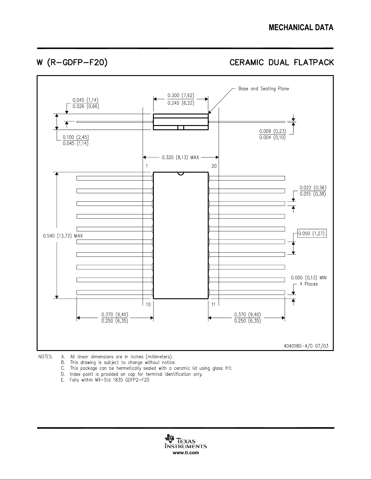
MECHANICAL DATA
MLCC006B – OCTOBER 1996
FK (S-CQCC-N**) LEADLESS CERAMIC CHIP CARRIER
28 TERMINAL SHOWN
A SQ
B SQ
19
20
21
22
23
24
25
12826 27
12
1314151618 17
0.020 (0,51)
0.010 (0,25)
MIN
0.342
(8,69)
0.442
0.640
0.739
0.938
1.141
A
0.358
(9,09)
0.458
(11,63)
0.660
(16,76)
0.761
(19,32)(18,78)
0.962
(24,43)
1.165
(29,59)
NO. OF
TERMINALS
**
11
10
9
8
7
6
5
432
20
28
44
52
68
84
0.020 (0,51)
0.010 (0,25)
(11,23)
(16,26)
(23,83)
(28,99)
MINMAX
0.307
(7,80)
0.406
(10,31)
0.495
(12,58)
0.495
(12,58)
0.850
(21,6)
1.047
(26,6)
0.080 (2,03)
0.064 (1,63)
B
MAX
0.358
(9,09)
0.458
(11,63)
0.560
(14,22)
0.560
(14,22)
0.858
(21,8)
1.063
(27,0)
0.055 (1,40)
0.045 (1,14)
0.028 (0,71)
0.022 (0,54)
0.050 (1,27)
NOTES: A. All linear dimensions are in inches (millimeters).
B. This drawing is subject to change without notice.
C. This package can be hermetically sealed with a metal lid.
D. The terminals are gold plated.
E. Falls within JEDEC MS-004
POST OFFICE BOX 655303 • DALLAS, TEXAS 75265
0.045 (1,14)
0.035 (0,89)
0.045 (1,14)
0.035 (0,89)
4040140/D 10/96
Page 20

Page 21

Page 22
Page 23

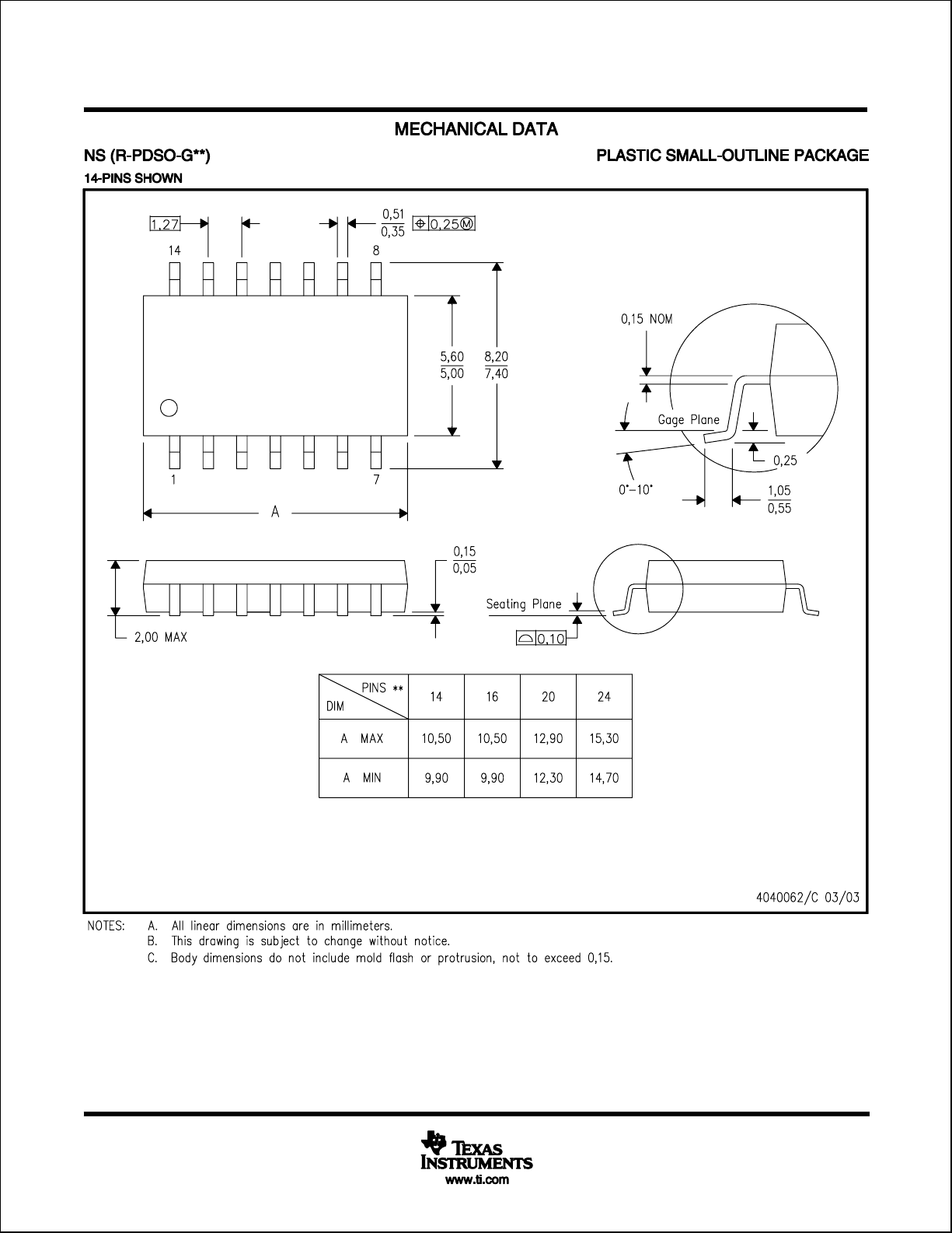
MECHANICAL DATA
MSSO002E – JANUARY 1995 – REVISED DECEMBER 2001
DB (R-PDSO-G**) PLASTIC SMALL-OUTLINE
28 PINS SHOWN
0,65
28
1
2,00 MAX
0,38
0,22
15
14
A
0,05 MIN
0,15
5,60
5,00
M
8,20
7,40
Seating Plane
0,10
0,25
0,09
0°–ā8°
Gage Plane
0,25
0,95
0,55
PINS **
DIM
A MAX
A MIN
NOTES: A. All linear dimensions are in millimeters.
B. This drawing is subject to change without notice.
C. Body dimensions do not include mold flash or protrusion not to exceed 0,15.
D. Falls within JEDEC MO-150
14
6,50
6,50
5,905,90
2016
7,50
6,90
24
8,50
28
10,50
9,907,90
30
10,50
9,90
38
12,90
12,30
4040065 /E 12/01
POST OFFICE BOX 655303 • DALLAS, TEXAS 75265
Page 24

IMPORTANT NOTICE
Texas Instruments Incorporated and its subsidiaries (TI) reserve the right to make corrections, modifications,
enhancements, improvements, and other changes to its products and services at any time and to discontinue
any product or service without notice. Customers should obtain the latest relevant information before placing
orders and should verify that such information is current and complete. All products are sold subject to TI’s terms
and conditions of sale supplied at the time of order acknowledgment.
TI warrants performance of its hardware products to the specifications applicable at the time of sale in
accordance with TI’s standard warranty. Testing and other quality control techniques are used to the extent TI
deems necessary to support this warranty . Except where mandated by government requirements, testing of all
parameters of each product is not necessarily performed.
TI assumes no liability for applications assistance or customer product design. Customers are responsible for
their products and applications using TI components. To minimize the risks associated with customer products
and applications, customers should provide adequate design and operating safeguards.
TI does not warrant or represent that any license, either express or implied, is granted under any TI patent right,
copyright, mask work right, or other TI intellectual property right relating to any combination, machine, or process
in which TI products or services are used. Information published by TI regarding third-party products or services
does not constitute a license from TI to use such products or services or a warranty or endorsement thereof.
Use of such information may require a license from a third party under the patents or other intellectual property
of the third party, or a license from TI under the patents or other intellectual property of TI.
Reproduction of information in TI data books or data sheets is permissible only if reproduction is without
alteration and is accompanied by all associated warranties, conditions, limitations, and notices. Reproduction
of this information with alteration is an unfair and deceptive business practice. TI is not responsible or liable for
such altered documentation.
Resale of TI products or services with statements different from or beyond the parameters stated by TI for that
product or service voids all express and any implied warranties for the associated TI product or service and
is an unfair and deceptive business practice. TI is not responsible or liable for any such statements.
Following are URLs where you can obtain information on other Texas Instruments products and application
solutions:
Products Applications
Amplifiers amplifier.ti.com Audio www.ti.com/audio
Data Converters dataconverter.ti.com Automotive www.ti.com/automotive
DSP dsp.ti.com Broadband www.ti.com/broadband
Interface interface.ti.com Digital Control www.ti.com/digitalcontrol
Logic logic.ti.com Military www.ti.com/military
Power Mgmt power.ti.com Optical Networking www.ti.com/opticalnetwork
Microcontrollers microcontroller.ti.com Security www.ti.com/security
Telephony www.ti.com/telephony
Video & Imaging www.ti.com/video
Wireless www.ti.com/wireless
Mailing Address: Texas Instruments
Post Office Box 655303 Dallas, Texas 75265
Copyright 2005, Texas Instruments Incorporated
 Loading...