

Texas Instruments SN54HC193J, SN74HC193D, SN74HC193DR, SN74HC193N, SN74HC193NSR Datasheet
...
SN54HC193, SN74HC193
4-BIT SYNCHRONOUS UP/DOWN COUNTERS
(DUAL CLOCK WITH CLEAR)
SCLS122B – DECEMBER 1982 – REVISED MA Y 1997
D
Look-Ahead Circuitry Enhances Cascaded
Counters
D
Fully Synchronous in Count Modes
D
Parallel Asynchronous Load for Modulo-N
Count Lengths
D
Asynchronous Clear
D
Package Options Include Plastic
Small-Outline (D) and Ceramic Flat (W)
Packages, Ceramic Chip Carriers (FK), and
Standard Plastic (N) and Ceramic (J)
300-mil DIPs
description
The ’HC193 are 4-bit synchronous, reversible,
up/down binary counters. Synchronous operation
is provided by having all flip-flops clocked
simultaneously so that the outputs change
coincidentally with each other when so instructed
by the steering logic. This mode of operation
eliminates the output counting spikes normally
associated with asynchronous (ripple-clock)
counters.
The outputs of the four flip-flops are triggered on
a low-to-high-level transition of either count
(clock) input (UP or DOWN). The direction of
counting is determined by which count input is
pulsed while the other count input is high.
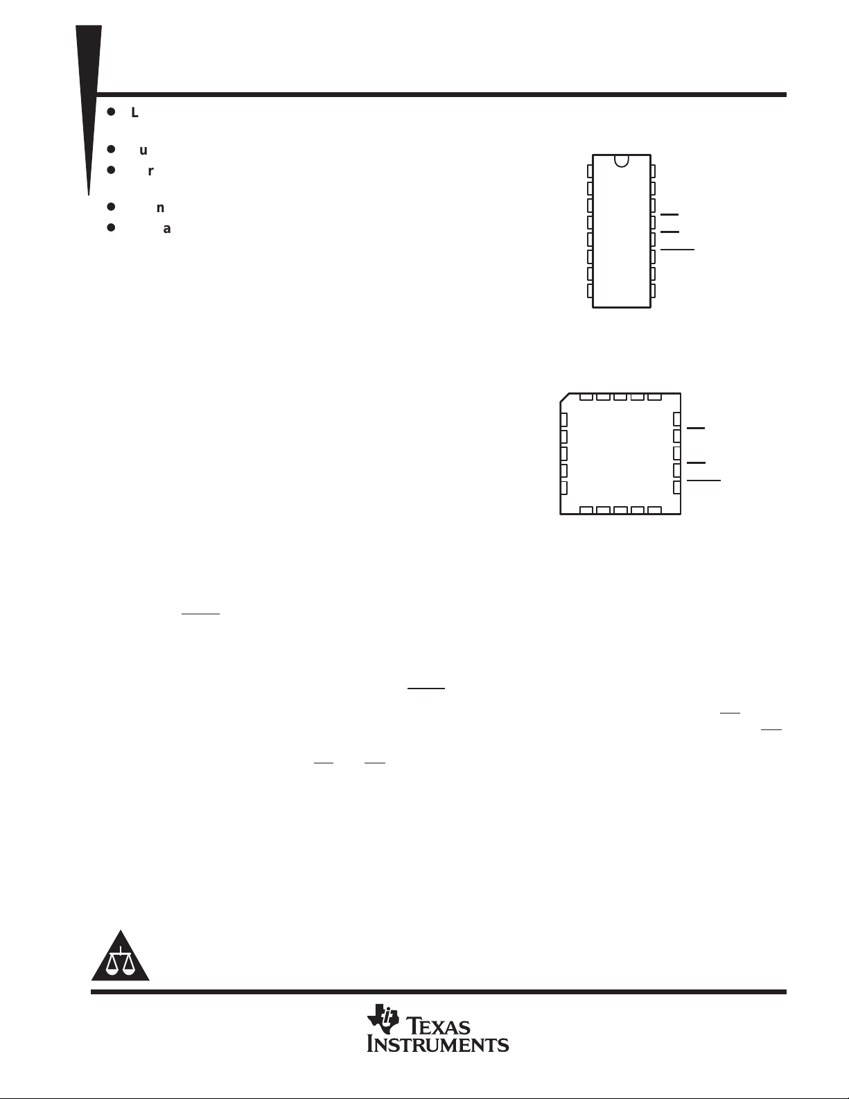
SN54HC193 ...J OR W PACKAGE
SN74HC193 ...D OR N PACKAGE
DOWN
SN54HC193 . . . FK PACKAGE
Q
A
DOWN
NC
UP
Q
C
NC – No internal connection
(TOP VIEW)
B
1
Q
2
B
Q
3
A
4
5
UP
6
Q
C
7
Q
D
GND
8
(TOP VIEW)
B
QBNC
3212019
4
5
6
7
8
910111213
D
Q
GND
NC
16
15
14
13
12
11
10
9
V
D
CC
V
CC
A
CLR
BO
CO
LOAD
C
D
A
18
17
16
15
14
C
CLR
BO
NC
CO
LOAD
All four counters are fully programmable; that is, each output may be preset to either level by placing a low on
the load (LOAD
) input and entering the desired data at the data inputs. The output changes to agree with the
data inputs independently of the count pulses. This feature allows the counters to be used as modulo-N dividers
by simply modifying the count length with the preset inputs.
A clear (CLR) input has been provided that forces all outputs to the low level when a high level is applied. The
clear function is independent of the count and LOAD
inputs.
These counters were designed to be cascaded without the need for external circuitry . The borrow (BO) output
produces a low-level pulse while the count is zero (all outputs low) and DOWN is low. Similarly, the carry (CO)
output produces a low-level pulse while the count is maximum (9 or 15) and UP is low. The counters can then
be easily cascaded by feeding BO and CO to DOWN and UP, respectively , of the succeeding counter.
The SN54HC193 is characterized for operation over the full military temperature range of –55°C to 125°C. The
SN74HC193 is characterized for operation from –40°C to 85°C.
Please be aware that an important notice concerning availability, standard warranty, and use in critical applications of
Texas Instruments semiconductor products and disclaimers thereto appears at the end of this data sheet.
PRODUCTION DATA information is current as of publication date.
Products conform to specifications per the terms of Texas Instruments
standard warranty. Production processing does not necessarily include
testing of all parameters.
Copyright 1997, Texas Instruments Incorporated
POST OFFICE BOX 655303 • DALLAS, TEXAS 75265
1
SN54HC193, SN74HC193
4-BIT SYNCHRONOUS UP/DOWN COUNTERS
(DUAL CLOCK WITH CLEAR)
SCLS122B – DECEMBER 1982 – REVISED MA Y 1997
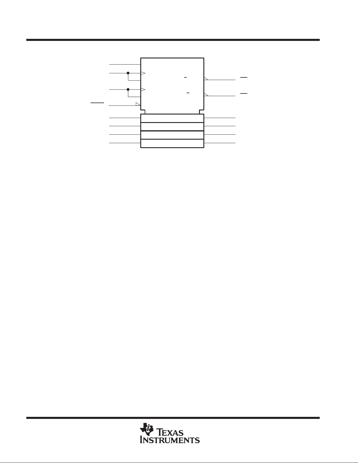
logic symbol
†
This symbol is in accordance with ANSI/IEEE Std 91-1984 and IEC Publication 617-12.
Pin numbers shown are for the D, J, N, and W packages.
†
CLR
UP
DOWN
LOAD
14
5
4
11
15
A
1
B
10
C
9
D
CT=0
G1
G2
C3
3D
2+
1–
CTRDIV16
[1]
[2]
[4]
[8]
1CT=15
2
CT=0
12
13
CO
BO
3
Q
A
2
Q
B
6
Q
C
7
Q
D
2
POST OFFICE BOX 655303 • DALLAS, TEXAS 75265
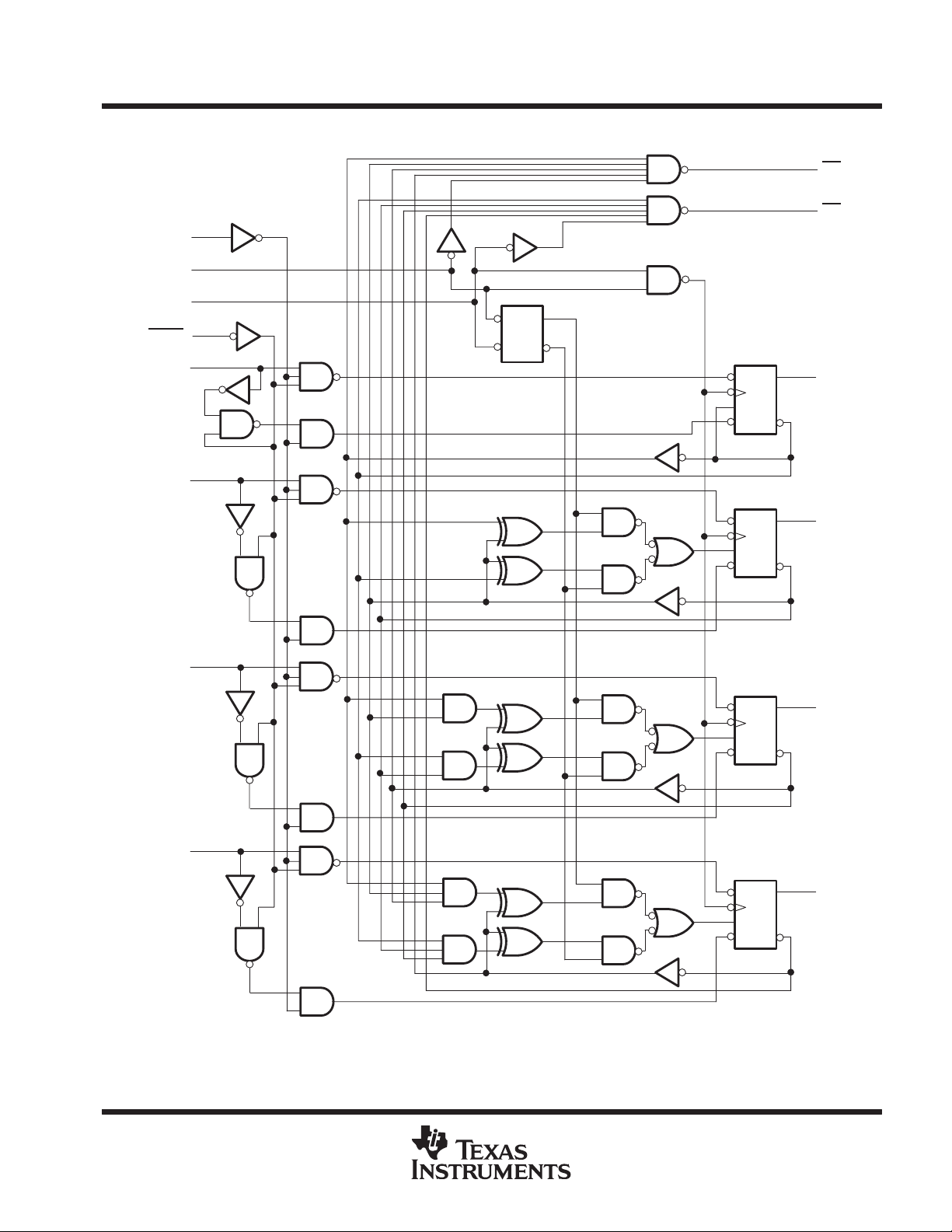
logic diagram (positive logic)
14
CLR
5
UP
DOWN
LOAD
4
11
15
A
1
B
SN54HC193, SN74HC193
4-BIT SYNCHRONOUS UP/DOWN COUNTERS
(DUAL CLOCK WITH CLEAR)
SCLS122B – DECEMBER 1982 – REVISED MA Y 1997
12
CO
13
BO
S
R
3
S
C1
1D
R
Q
A
2
S
C1
1D
R
10
C
S
C1
1D
R
9
D
S
C1
1D
R
Q
B
6
Q
C
7
Q
D
Pin numbers shown are for the D, J, N, and W packages.
POST OFFICE BOX 655303 • DALLAS, TEXAS 75265
3
SN54HC193, SN74HC193
4-BIT SYNCHRONOUS UP/DOWN COUNTERS
(DUAL CLOCK WITH CLEAR)
SCLS122B – DECEMBER 1982 – REVISED MA Y 1997
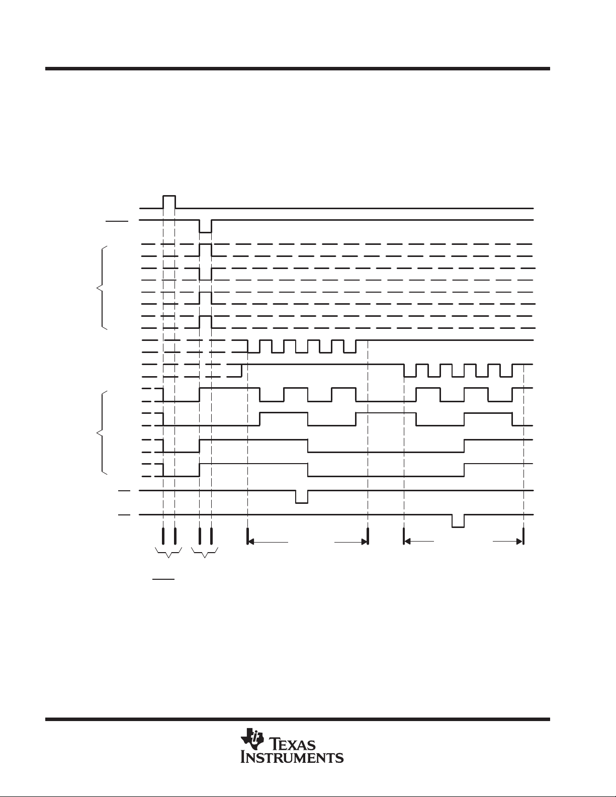
typical clear, load, and count sequence
The following sequence is illustrated below:
1. Clear outputs to 0
2. Load (preset) to binary 13
3. Count up to 14, 15, carry, 0, 1, and 2
4. Count down to 1, 0, borrow, 15, 14, and 13
CLR
LOAD
A
Data
Inputs
Data
Outputs
UP
DOWN
Q
Q
Q
Q
CO
BO
B
C
D
A
B
C
D
013 14 012
Clear
Preset
15 1 0
Count Up
15 14 13
Count Down
NOTES: A. CLR overrides LOAD
B. When counting up, count-down input must be high; when counting down, count-up input must be high.
4
, data, and count inputs.
POST OFFICE BOX 655303 • DALLAS, TEXAS 75265

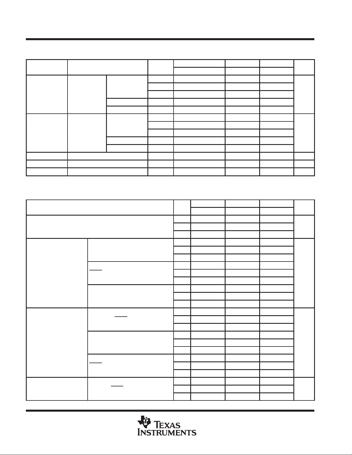
UNIT
‡
SN54HC193, SN74HC193
4-BIT SYNCHRONOUS UP/DOWN COUNTERS
(DUAL CLOCK WITH CLEAR)
SCLS122B – DECEMBER 1982 – REVISED MA Y 1997
absolute maximum ratings over operating free-air temperature range
Supply voltage range, V
–0.5 V to 7 V. . . . . . . . . . . . . . . . . . . . . . . . . . . . . . . . . . . . . . . . . . . . . . . . . . . . . . . . . .
CC
†
Input clamp current, IIK (VI < 0 or VI > VCC) (see Note 1) ±20 mA. . . . . . . . . . . . . . . . . . . . . . . . . . . . . . . . . . . .
Output clamp current, IOK (VO < 0 or VO > VCC) (see Note 1) ±20 mA. . . . . . . . . . . . . . . . . . . . . . . . . . . . . . . .
Continuous output current, IO (VO = 0 to VCC) ±25 mA. . . . . . . . . . . . . . . . . . . . . . . . . . . . . . . . . . . . . . . . . . . . . .
Continuous current through VCC or GND ±50 mA. . . . . . . . . . . . . . . . . . . . . . . . . . . . . . . . . . . . . . . . . . . . . . . . . . .
Package thermal impedance, θ
(see Note 2): D package 113°C/W. . . . . . . . . . . . . . . . . . . . . . . . . . . . . . . . . .
JA
N package 78°C/W. . . . . . . . . . . . . . . . . . . . . . . . . . . . . . . . . . .
Storage temperature range, T
†
Stresses beyond those listed under “absolute maximum ratings” may cause permanent damage to the device. These are stress ratings only, and
functional operation of the device at these or any other conditions beyond those indicated under “recommended operating conditions” is not
implied. Exposure to absolute-maximum-rated conditions for extended periods may affect device reliability.
NOTES: 1. The input and output voltage ratings may be exceeded if the input and output current ratings are observed.
2. The package thermal impedance is calculated in accordance with JESD 51, except for through-hole packages, which use a trace
length of zero.
–65°C to 150°C. . . . . . . . . . . . . . . . . . . . . . . . . . . . . . . . . . . . . . . . . . . . . . . . . . .
stg
recommended operating conditions
SN54HC193 SN74HC193
MIN NOM MAX MIN NOM MAX
V
V
V
V
V
t
t
T
‡
If this device is used in the threshold region (from VILmax = 0.5 V to VIHmin = 1.5 V), there is a potential to go into the wrong state from induced
grounding, causing double clocking. Operating with the inputs at tt = 1000 ns and VCC = 2 V does not damage the device; however, functionally ,
the CLK inputs are not ensured while in the shift, count, or toggle operating modes.
Supply voltage 2 5 6 2 5 6 V
CC
VCC = 2 V 1.5 1.5
High-level input voltage
IH
Low-level input voltage
IL
Input voltage 0 V
I
Output voltage 0 V
O
Input transition (rise and fall) time
Operating free-air temperature –55 125 –40 85 °C
A
VCC = 4.5 V
VCC = 6 V 4.2 4.2
VCC = 2 V 0 0.5 0 0.5
VCC = 4.5 V
VCC = 6 V 0 1.8 0 1.8
VCC = 2 V 0 1000 0 1000
VCC = 4.5 V
VCC = 6 V 0 400 0 400
3.15 3.15
0 1.35 0 1.35
CC
CC
0 500 0 500
0 V
0 V
CC
CC
V
V
V
V
ns
POST OFFICE BOX 655303 • DALLAS, TEXAS 75265
5
SN54HC193, SN74HC193
PARAMETER
TEST CONDITIONS
V
UNIT
V
UNIT
↑
↑
4-BIT SYNCHRONOUS UP/DOWN COUNTERS
(DUAL CLOCK WITH CLEAR)
SCLS122B – DECEMBER 1982 – REVISED MA Y 1997
electrical characteristics over recommended operating free-air temperature range (unless
otherwise noted)
TA = 25°C SN54HC193 SN74HC193
MIN TYP MAX MIN MAX MIN MAX
V
V
V
V
I
I
C
OH
OL
I
CC
CC
2 V 1.9 1.998 1.9 1.9
IOH = –20 µA
VI = VIH or V
VI = VIH or V
VI = VCC or 0 6 V ±0.1 ±100 ±1000 ±1000 nA
VI = VCC or 0, IO = 0 6 V 8 160 80 µA
i
IL
IOH = –4 mA 4.5 V 3.98 4.3 3.7 3.84
IOH = –5.2 mA 6 V 5.48 5.8 5.2 5.34
IOL = 20 µA
IL
IOL = 4 mA 4.5 V 0.17 0.26 0.4 0.33
IOL = 5.2 mA 6 V 0.15 0.26 0.4 0.33
4.5 V 4.4 4.499 4.4 4.4
6 V 5.9 5.999 5.9 5.9
2 V 0.002 0.1 0.1 0.1
4.5 V 0.001 0.1 0.1 0.1
6 V 0.001 0.1 0.1 0.1
2 V to 6 V 3 10 10 10 pF
timing requirements over recommended operating free-air temperature range (unless otherwise
noted)
TA = 25°C SN54HC193 SN74HC193
CC
MIN MAX MIN MAX MIN MAX
2 V 0 4.2 0 2.8 0 3.3
f
clock
t
w
t
su
t
h
Clock frequency
CLR high
Pulse duration LOAD low
UP or DOWN high or low
Data before LOAD inactive
Setup time CLR inactive before UP↑ or DOWN
LOAD inactive before UP↑ or DOWN
Hold time Data after LOAD inactive
4.5 V
6 V 0 24 0 16 0 19
2 V 120 180 150
4.5 V 24 36 30
6 V 21 31 26
2 V 120 180 150
4.5 V 24 36 30
6 V 21 31 26
2 V 120 180 150
4.5 V 24 36 30
6 V 21 31 26
2 V 110 165 140
4.5 V 22 33 28
6 V 19 28 24
2 V 110 165 140
4.5 V 22 33 28
6 V 19 28 24
2 V 110 165 140
4.5 V 22 33 28
6 V 19 28 24
2 V 5 5 5
4.5 V 5 5 5
6 V 5 5 5
0 21 0 14 0 17
MHz
ns
ns
ns
6
POST OFFICE BOX 655303 • DALLAS, TEXAS 75265
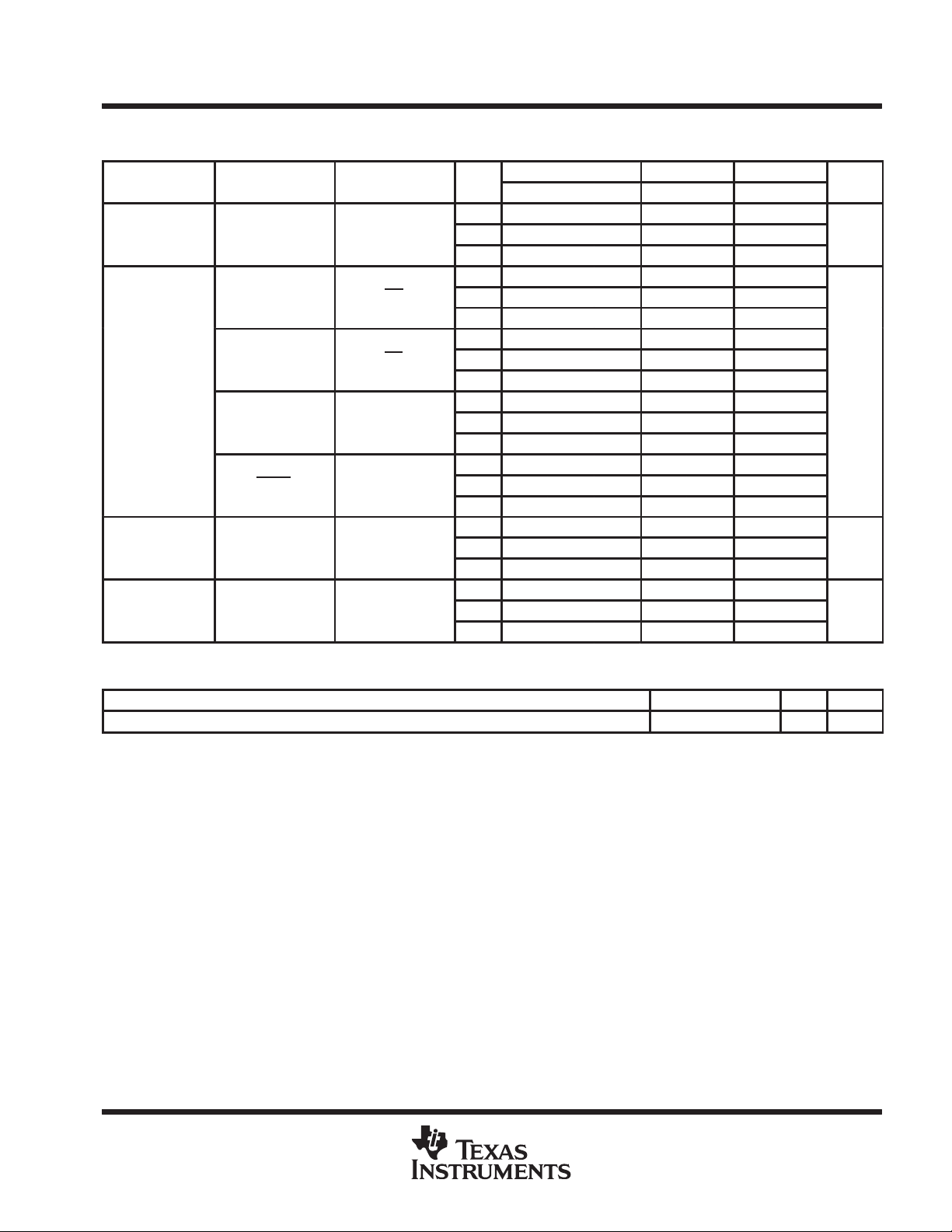
PARAMETER
V
UNIT
t
ns
SN54HC193, SN74HC193
4-BIT SYNCHRONOUS UP/DOWN COUNTERS
(DUAL CLOCK WITH CLEAR)
SCLS122B – DECEMBER 1982 – REVISED MA Y 1997
switching characteristics over recommended operating free-air temperature range, CL = 50 pF
(unless otherwise noted) (see Figure 1)
TA = 25°C SN54HC193 SN74HC193
MIN TYP MAX MIN MAX MIN MAX
MHz
ns
ns
f
max
pd
t
PHL
t
t
FROM TO
(INPUT) (OUTPUT)
UP CO
DOWN BO
UP or DOWN Any Q
LOAD Any Q
CLR Any Q
Any
CC
2 V 4.2 8 2.8 3.3
4.5 V 21 55 14 17
6 V 24 60 16 19
2 V 75 165 250 205
4.5 V 24 33 50 41
6 V 20 28 43 35
2 V 75 165 250 205
4.5 V 24 33 50 41
6 V 20 28 43 35
2 V 190 250 375 315
4.5 V 40 50 75 63
6 V 35 43 64 54
2 V 190 260 390 325
4.5 V 40 52 78 65
6 V 35 44 66 55
2 V 170 240 360 300
4.5 V 36 48 72 60
6 V 31 41 61 51
2 V 38 75 110 95
4.5 V 8 15 22 19
6 V 6 13 19 16
operating characteristics, TA = 25°C
PARAMETER TEST CONDITIONS TYP UNIT
C
Power dissipation capacitance No load 50 pF
pd
POST OFFICE BOX 655303 • DALLAS, TEXAS 75265
7
SN54HC193, SN74HC193
4-BIT SYNCHRONOUS UP/DOWN COUNTERS
(DUAL CLOCK WITH CLEAR)
SCLS122B – DECEMBER 1982 – REVISED MA Y 1997
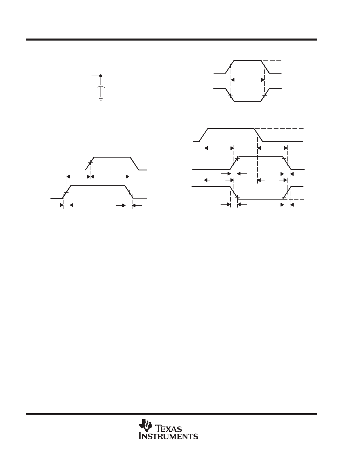
PARAMETER MEASUREMENT INFORMATION
50%
Test
Point
CL = 50 pF
(see Note A)
t
h
V
CC
0 V
V
CC
50%50%
10%10%
t
f
Out-of-Phase
0 V
From Output
Under Test
LOAD CIRCUIT
Reference
Input
t
su
Data
Input
SETUP AND HOLD AND INPUT RISE AND FALL TIMES
90% 90%
t
r
VOLTAGE WAVEFORMS
High-Level
Pulse
Low-Level
Pulse
Input
In-Phase
Output
Output
PROPAGATION DELAY AND OUTPUT TRANSITION TIMES
50%
t
t
PLH
PHL
50%
t
w
50%
VOLTAGE WAVEFORMS
PULSE DURATIONS
50%
90% 90%
t
r
t
50% 50%
10% 10%
t
f
VOLTAGE WAVEFORMS
50%
50%
t
PHL
PLH
V
0 V
V
0 V
CC
CC
V
CC
0 V
V
50%50%
OH
10%10%
V
OL
t
f
V
OH
90%90%
V
OL
t
r
NOTES: A. CL includes probe and test-fixture capacitance.
B. Phase relationships between waveforms were chosen arbitrarily. All input pulses are supplied by generators having the following
characteristics: PRR ≤ 1 MHz, ZO = 50 Ω, tr = 6 ns, tf = 6 ns.
C. For clock inputs, f
D. The outputs are measured one at a time with one input transition per measurement.
E. t
PLH
and t
PHL
is measured when the input duty cycle is 50%.
max
are the same as tpd.
Figure 1. Load Circuit and Voltage Waveforms
8
POST OFFICE BOX 655303 • DALLAS, TEXAS 75265

IMPORTANT NOTICE
T exas Instruments and its subsidiaries (TI) reserve the right to make changes to their products or to discontinue
any product or service without notice, and advise customers to obtain the latest version of relevant information
to verify, before placing orders, that information being relied on is current and complete. All products are sold
subject to the terms and conditions of sale supplied at the time of order acknowledgement, including those
pertaining to warranty, patent infringement, and limitation of liability.
TI warrants performance of its semiconductor products to the specifications applicable at the time of sale in
accordance with TI’s standard warranty. Testing and other quality control techniques are utilized to the extent
TI deems necessary to support this warranty . Specific testing of all parameters of each device is not necessarily
performed, except those mandated by government requirements.
CERTAIN APPLICATIONS USING SEMICONDUCTOR PRODUCTS MAY INVOLVE POTENTIAL RISKS OF
DEATH, PERSONAL INJURY, OR SEVERE PROPERTY OR ENVIRONMENTAL DAMAGE (“CRITICAL
APPLICATIONS”). TI SEMICONDUCTOR PRODUCTS ARE NOT DESIGNED, AUTHORIZED, OR
WARRANTED TO BE SUITABLE FOR USE IN LIFE-SUPPORT DEVICES OR SYSTEMS OR OTHER
CRITICAL APPLICA TIONS. INCLUSION OF TI PRODUCTS IN SUCH APPLICATIONS IS UNDERST OOD TO
BE FULLY AT THE CUSTOMER’S RISK.
In order to minimize risks associated with the customer’s applications, adequate design and operating
safeguards must be provided by the customer to minimize inherent or procedural hazards.
TI assumes no liability for applications assistance or customer product design. TI does not warrant or represent
that any license, either express or implied, is granted under any patent right, copyright, mask work right, or other
intellectual property right of TI covering or relating to any combination, machine, or process in which such
semiconductor products or services might be or are used. TI’s publication of information regarding any third
party’s products or services does not constitute TI’s approval, warranty or endorsement thereof.
Copyright 1998, Texas Instruments Incorporated
 Loading...