

Page 1
SN54F244, SN74F244
OCTAL BUFFERS/DRIVERS
WITH 3-STATE OUTPUTS
SDFS063A – D2932, MARCH 1987 – REVISED OCT OBER 1993
• 3-State Outputs Drive Bus Lines or Buffer
Memory Address Registers
• Package Options Include Plastic
Small-Outline (SOIC) and Shrink
Small-Outline (SSOP) Packages, Ceramic
Chip Carriers, and Plastic and Ceramic
DIPs
description
These octal buffers and line drivers are designed
specifically to improve both the performance and
density of 3-state memory address drivers, clock
drivers, and bus-oriented receivers and
transmitters. Taken together with the ′F240 and
′F241, these devices provide the choice of
selected combinations of inverting and
noninverting outputs, symmetrical OE
output-enable) inputs, and complementary OE
and OE
The ′F244 is organized as two 4-bit buffers/line
drivers with separate output enable (OE
When OE
A inputs to the Y outputs. When OE
outputs are in the high-impedance state.
The SN74F244 is available in TI’s shrink
small-outline package (DB), which provides the
same I/O pin count and functionality of standard
small-outline packages in less than half the
printed-circuit-board area.
inputs.
is low, the device passes data from the
(active-low
) inputs.
is high, the
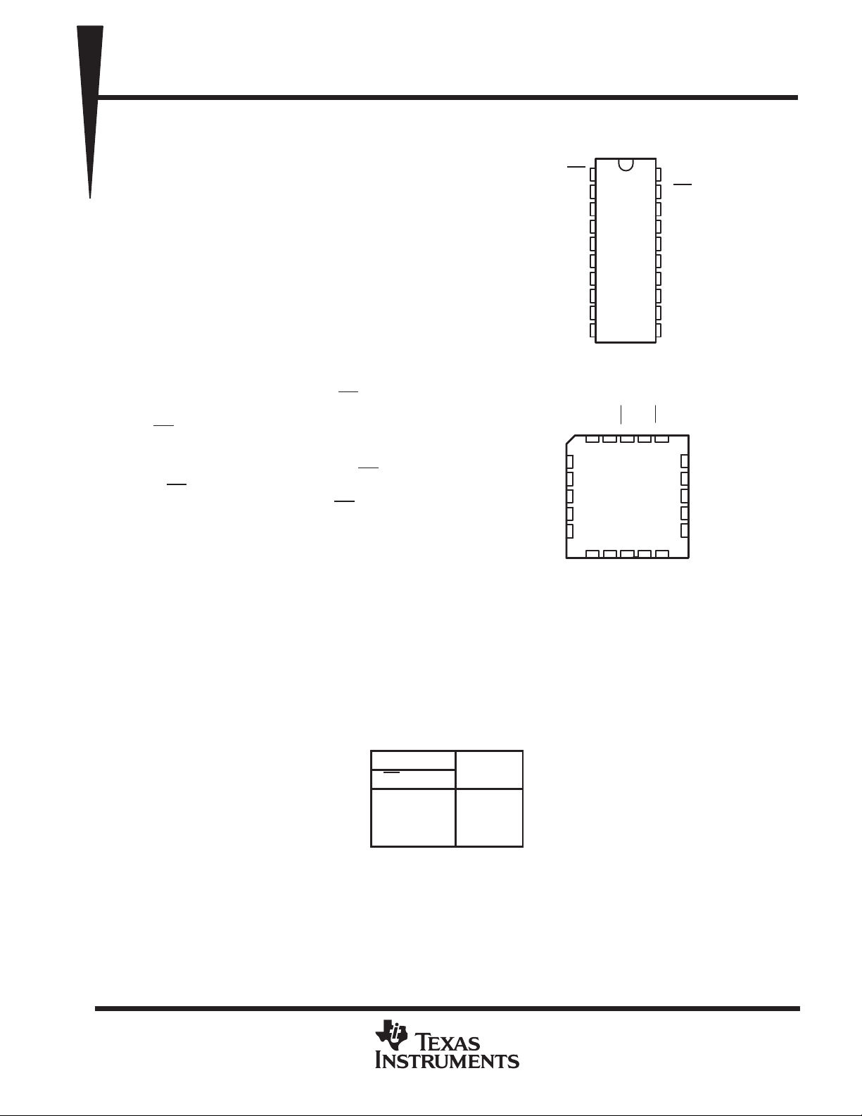
SN54F244 ...J PACKAGE
SN74F244 . . . DB, DW, OR N PACKAGE
1A2
2Y3
1A3
2Y2
1A4
(TOP VIEW)
1OE
1
1A1
2
2Y4
3
1A2
4
2Y3
5
1A3
6
2Y2
7
1A4
8
9
2Y1
GND
SN54F244 . . . FK PACKAGE
10
(TOP VIEW)
2Y4
1A1
3 2 1 20 19
4
5
6
7
8
9 10 11 12 13
2Y1
GND
20
19
18
17
16
15
14
13
12
11
V
1OE
2A1
CC
1Y4
V
CC
2OE
1Y1
2A4
1Y2
2A3
1Y3
2A2
1Y4
2A1
18
17
16
15
14
2A2 2OE
1Y1
2A4
1Y2
2A3
1Y3
The SN54F244 is characterized for operation over
the full military temperature range of –55°C to
125°C. The SN74F244 is characterized for
operation from 0°C to 70°C.
PRODUCTION DATA information is current as of publication date.
Products conform to specifications per the terms of Texas Instruments
standard warranty. Production processing does not necessarily include
testing of all parameters.
FUNCTION TABLE
(each buffer)
INPUTS
OE A
L H H
L LL
HXZ
OUTPUT
Y
Copyright 1993, Texas Instruments Incorporated
POST OFFICE BOX 655303 • DALLAS, TEXAS 75265
2–1
Page 2
SN54F244, SN74F244
OCTAL BUFFERS/DRIVERS
WITH 3-STATE OUTPUTS
SDFS063A – D2932, MARCH 1987 – REVISED OCT OBER 1993
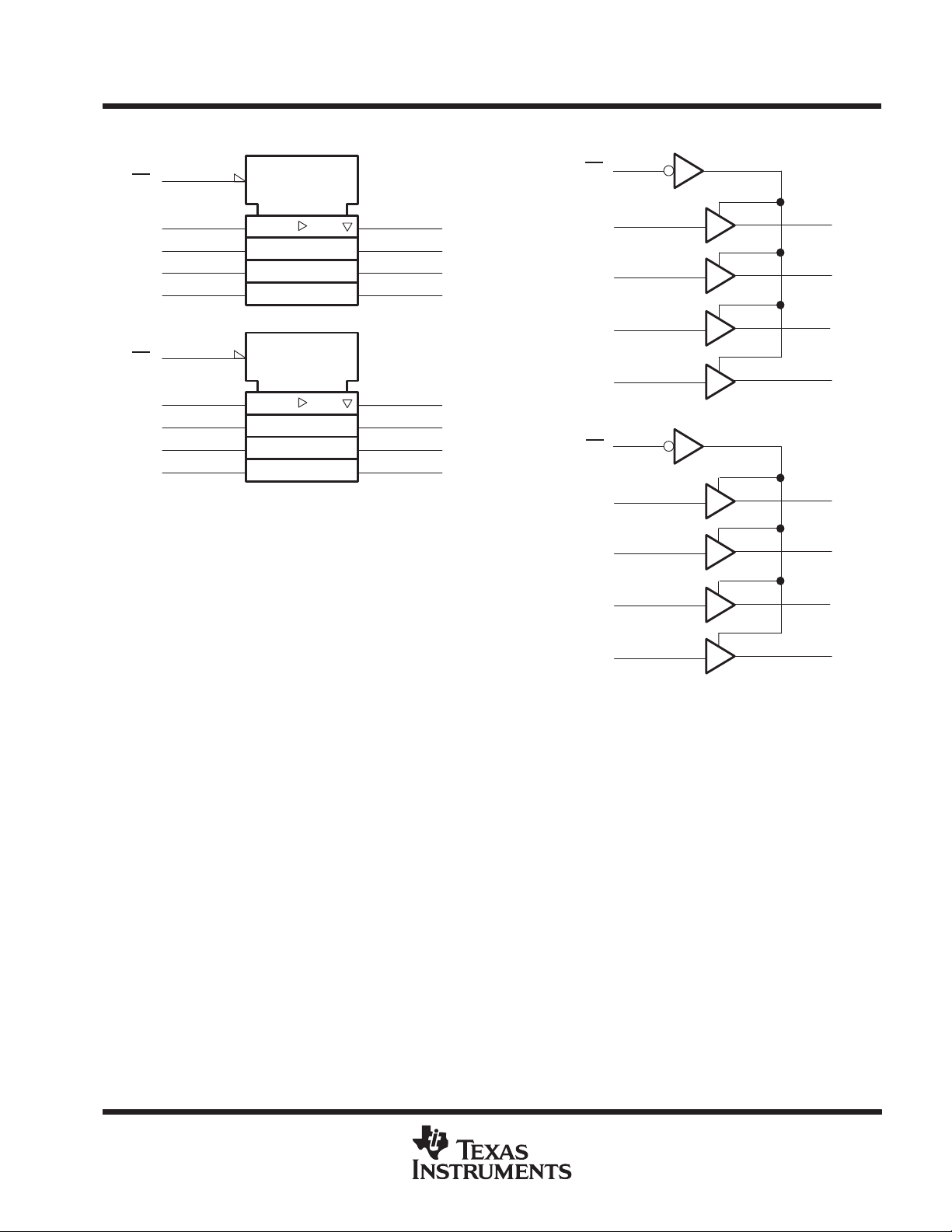
1
2
4
6
8
19
11
13
15
17
†
EN
EN
logic symbol
1OE
1A1
1A2
1A3
1A4
2OE
2A1
2A2
2A3
2A4
†
This symbol is in accordance with ANSI/IEEE Std 91-1984
and IEC Publication 617-12.
18
16
14
12
logic diagram (positive logic)
1OE
1Y1
1Y2
1Y3
1Y4
9
2Y1
7
2Y2
5
2Y3
3
2Y4
1A1
1A2
1A3
1A4
2OE
2A1
2A2
1
2
4
6
8
19
11
13
18
16
14
12
1Y1
1Y2
1Y3
1Y4
9
2Y1
7
2Y2
2A3
2A4
15
17
5
2Y3
3
2Y4
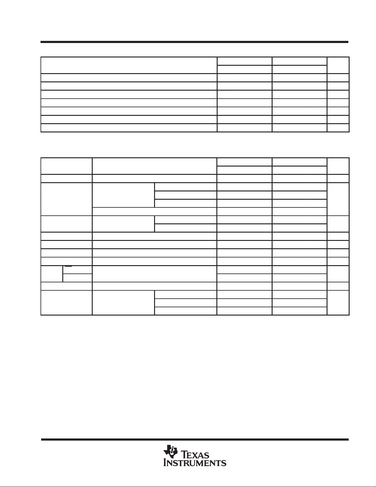
absolute maximum ratings over operating free-air temperature range (unless otherwise noted)
Supply voltage range, V
Input voltage range, V
Input current range –30 mA to 5 mA. . . . . . . . . . . . . . . . . . . . . . . . . . . . . . . . . . . . . . . . . . . . . . . . . . . . . . . . . . . . . .
Voltage range applied to any output in the disabled or power-off state –0.5 V to 5.5 V. . . . . . . . . . . . . . . . . . .
Voltage range applied to any output in the high state –0.5 V to V
Current into any output in the low state: SN54F244 96 mA. . . . . . . . . . . . . . . . . . . . . . . . . . . . . . . . . . . . . . . . . . .
Operating free-air temperature range: SN54F244 –55°C to 125°C. . . . . . . . . . . . . . . . . . . . . . . . . . . . . . . . . .
Storage temperature range –65°C to 150°C. . . . . . . . . . . . . . . . . . . . . . . . . . . . . . . . . . . . . . . . . . . . . . . . . . . . . . .
‡
Stresses beyond those listed under “absolute maximum ratings” may cause permanent damage to the device. These are stress ratings only and
functional operation of the device at these or any other conditions beyond those indicated under “recommended operating conditions” is not
implied. Exposure to absolute-maximum-rated conditions for extended periods may affect device reliability.
NOTE 1: The input voltage ratings may be exceeded provided the input current ratings are observed.
–0.5 V to 7 V. . . . . . . . . . . . . . . . . . . . . . . . . . . . . . . . . . . . . . . . . . . . . . . . . . . . . . . . . .
CC
(see Note 1) –1.2 V to 7 V. . . . . . . . . . . . . . . . . . . . . . . . . . . . . . . . . . . . . . . . . . . . . . . . . .
I
. . . . . . . . . . . . . . . . . . . . . . . . . . . . . . . . . .
SN74F244 128 mA. . . . . . . . . . . . . . . . . . . . . . . . . . . . . . . . . . . . . . . . . .
SN74F244 0°C to 70°C. . . . . . . . . . . . . . . . . . . . . . . . . . . . . . . . . . . . . .
‡
CC
2–2
POST OFFICE BOX 655303 • DALLAS, TEXAS 75265
Page 3
SN54F244, SN74F244
UNIT
PARAMETER
TEST CONDITIONS
UNIT
V
V
VOLV
V
V
I
V
5.5 V
V
0.5 V
mA
V
Out uts oen
OCTAL BUFFERS/DRIVERS
WITH 3-STATE OUTPUTS
SDFS063A – D2932, MARCH 1987 – REVISED OCTOBER 1993
recommended operating conditions
SN54F244 SN74F244
MIN NOM MAX MIN NOM MAX
V
CC
V
IH
V
IL
I
IK
I
OH
I
OL
T
A
electrical characteristics over recommended operating free-air temperature range (unless
otherwise noted)
V
IK
OH
I
OZH
I
OZL
I
I
I
IH
IL
I
OS
I
CC
†
All typical values are at VCC = 5 V, TA = 25°C.
‡
Not more than one output should be shorted at a time, and the duration of the short circuit should not exceed one second.
Supply voltage 4.5 5 5.5 4.5 5 5.5 V
High-level input voltage 2 2 V
Low-level input voltage 0.8 0.8 V
Input clamp current –18 –18 mA
High-level output current –12 –15 mA
Low-level output current 48 64 mA
Operating free-air temperature –55 125 0 70 °C
SN54F244 SN74F244
MIN TYP†MAX MIN TYP†MAX
VCC = 4.5 V, II = –18 mA –1.2 –1.2 V
IOH = – 3 mA 2.4 3.3 2.4 3.3
VCC = 4.5 V
VCC = 4.75 V, IOH = – 3 mA 2.7
= 4.5
CC
VCC = 5.5 V, VO = 2.7 V 50 50 µA
VCC = 5.5 V, VO = 0.5 V –50 –50 µA
VCC = 5.5 V, VI = 7 V 0.1 0.1 mA
VCC = 5.5 V, VI = 2.7 V 20 20 µA
OE
Any A
‡
CC
VCC = 5.5 V, VO = 0 –100 –225 –100 –225 mA
CC
p
=
= 5.5 V,
p
,
IOH = – 12 mA 2 3.2
IOH = – 15 mA 2 3.1
IOL = 48 mA 0.38 0.55
IOL = 64 mA 0.42 0.55
=
I
Outputs high 40 60 40 60
Outputs low 60 90 60 90
Outputs disabled 60 90 60 90
–1 –1
– 1.6 – 1.6
mA
POST OFFICE BOX 655303 • DALLAS, TEXAS 75265
2–3
Page 4
SN54F244, SN74F244
(
)
(
)
(INPUT)
(OUTPUT)
A
Y
ns
OE
Y
ns
OE
Y
ns
OCTAL BUFFERS/DRIVERS
WITH 3-STATE OUTPUTS
SDFS063A – D2932, MARCH 1987 – REVISED OCT OBER 1993
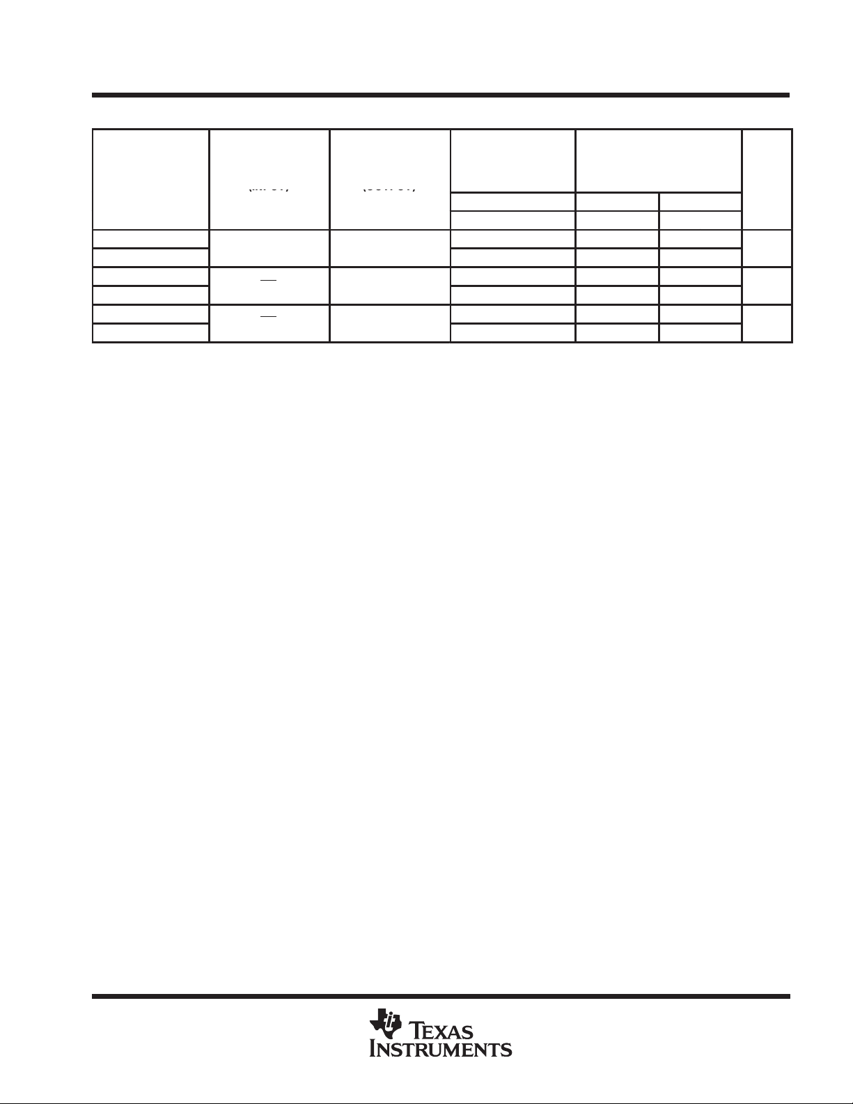
switching characteristics (see Note 2)
VCC = 5 V,
CL = 50 pF,
PARAMETER
t
PLH
t
PHL
t
PZH
t
PZL
t
PHZ
t
†
NOTE 2: Load circuits and waveforms are shown in Section 1.
PLZ
For conditions shown as MIN or MAX, use the appropriate value specified under recommended operating conditions.
FROM
INPUT
TO
OUTPUT
RL = 500 Ω,
TA = 25°C
′F244 SN54F244 SN74F244
MIN TYP MAX MIN MAX MIN MAX
1.7 3.6 5.2 2 6.5 1.7 6.2
1.7 3.6 5.2 2 7 1.7 6.5
1.2 3.9 5.7 2 7 1.2 6.7
1.2 5 7 2 8.5 1.2 8
1.2 4.1 6 2 7 1.2 7
1.2 4.1 6 2 7.5 1.2 7
VCC = 4.5 V to 5.5 V,
CL = 50 pF,
RL = 500Ω,
TA = MIN to MAX
†
UNIT
2–4
POST OFFICE BOX 655303 • DALLAS, TEXAS 75265
Page 5
PACKAGE OPTION ADDENDUM
www.ti.com
PACKAGING INFORMATION
Orderable Device Status
5962-9758601Q2A ACTIVE LCCC FK 20 1 TBD Call TI Level-NC-NC-NC
5962-9758601QRA ACTIVE CDIP J 20 1 TBD Call TI Level-NC-NC-NC
5962-9758601QRA ACTIVE CDIP J 20 1 TBD Call TI Level-NC-NC-NC
5962-9758601QSA ACTIVE CFP W 20 1 TBD Call TI Level-NC-NC-NC
5962-9758601QSA ACTIVE CFP W 20 1 TBD Call TI Level-NC-NC-NC
JM38510/33203B2A ACTIVE LCCC FK 20 1 TBD Call TI Level-NC-NC-NC
JM38510/33203B2A ACTIVE LCCC FK 20 1 TBD Call TI Level-NC-NC-NC
JM38510/33203BRA ACTIVE CDIP J 20 1 TBD Call TI Level-NC-NC-NC
JM38510/33203BRA ACTIVE CDIP J 20 1 TBD Call TI Level-NC-NC-NC
JM38510/33203BSA ACTIVE CFP W 20 1 TBD Call TI Level-NC-NC-NC
JM38510/33203BSA ACTIVE CFP W 20 1 TBD Call TI Level-NC-NC-NC
SN54F244J ACTIVE CDIP J 20 1 TBD Call TI Level-NC-NC-NC
SN54F244J ACTIVE CDIP J 20 1 TBD Call TI Level-NC-NC-NC
SN74F244DBLE OBSOLETE SSOP DB 20 TBD Call TI Call TI
SN74F244DBLE OBSOLETE SSOP DB 20 TBD Call TI Call TI
SN74F244DBR ACTIVE SSOP DB 20 2000 Green (RoHS &
SN74F244DBR ACTIVE SSOP DB 20 2000 Green (RoHS &
SN74F244DBRE4 ACTIVE SSOP DB 20 2000 Green (RoHS &
SN74F244DBRE4 ACTIVE SSOP DB 20 2000 Green (RoHS &
SN74F244DW ACTIVE SOIC DW 20 25 Green (RoHS &
SN74F244DW ACTIVE SOIC DW 20 25 Green (RoHS &
SN74F244DWG4 ACTIVE SOIC DW 20 25 Green (RoHS &
SN74F244DWG4 ACTIVE SOIC DW 20 25 Green (RoHS &
SN74F244DWR ACTIVE SOIC DW 20 2000 Green (RoHS &
SN74F244DWR ACTIVE SOIC DW 20 2000 Green (RoHS &
SN74F244DWRG4 ACTIVE SOIC DW 20 2000 Green (RoHS &
SN74F244DWRG4 ACTIVE SOIC DW 20 2000 Green (RoHS &
SN74F244N ACTIVE PDIP N 20 20 Pb-Free
SN74F244N ACTIVE PDIP N 20 20 Pb-Free
SN74F244N3 OBSOLETE PDIP N 20 TBD Call TI Call TI
SN74F244N3 OBSOLETE PDIP N 20 TBD Call TI Call TI
SN74F244NE4 ACTIVE PDIP N 20 20 Pb-Free CU NIPDAU Level-NC-NC-NC
(1)
Package
Type
Package
Drawing
Pins Package
Qty
Eco Plan
no Sb/Br)
no Sb/Br)
no Sb/Br)
no Sb/Br)
no Sb/Br)
no Sb/Br)
no Sb/Br)
no Sb/Br)
no Sb/Br)
no Sb/Br)
no Sb/Br)
no Sb/Br)
(RoHS)
(RoHS)
(2)
Lead/Ball Finish MSL Peak Temp
CU NIPDAU Level-1-260C-UNLIM
CU NIPDAU Level-1-260C-UNLIM
CU NIPDAU Level-1-260C-UNLIM
CU NIPDAU Level-1-260C-UNLIM
CU NIPDAU Level-1-260C-UNLIM
CU NIPDAU Level-1-260C-UNLIM
CU NIPDAU Level-1-260C-UNLIM
CU NIPDAU Level-1-260C-UNLIM
CU NIPDAU Level-1-260C-UNLIM
CU NIPDAU Level-1-260C-UNLIM
CU NIPDAU Level-1-260C-UNLIM
CU NIPDAU Level-1-260C-UNLIM
CU NIPDAU Level-NC-NC-NC
CU NIPDAU Level-NC-NC-NC
17-Oct-2005
(3)
Addendum-Page 1
Page 6

PACKAGE OPTION ADDENDUM
www.ti.com
Orderable Device Status
(1)
Package
Type
Package
Drawing
Pins Package
Qty
Eco Plan
(2)
Lead/Ball Finish MSL Peak Temp
17-Oct-2005
(3)
(RoHS)
SN74F244NE4 ACTIVE PDIP N 20 20 Pb-Free
CU NIPDAU Level-NC-NC-NC
(RoHS)
SN74F244NSR ACTIVE SO NS 20 2000 Green (RoHS &
CU NIPDAU Level-1-260C-UNLIM
no Sb/Br)
SN74F244NSR ACTIVE SO NS 20 2000 Green (RoHS &
CU NIPDAU Level-1-260C-UNLIM
no Sb/Br)
SN74F244NSRE4 ACTIVE SO NS 20 2000 Green (RoHS &
CU NIPDAU Level-1-260C-UNLIM
no Sb/Br)
SN74F244NSRE4 ACTIVE SO NS 20 2000 Green (RoHS &
CU NIPDAU Level-1-260C-UNLIM
no Sb/Br)
SNJ54F244FK ACTIVE LCCC FK 20 1 TBD Call TI Level-NC-NC-NC
SNJ54F244FK ACTIVE LCCC FK 20 1 TBD Call TI Level-NC-NC-NC
SNJ54F244J ACTIVE CDIP J 20 1 TBD Call TI Level-NC-NC-NC
SNJ54F244J ACTIVE CDIP J 20 1 TBD Call TI Level-NC-NC-NC
SNJ54F244W ACTIVE CFP W 20 1 TBD Call TI Level-NC-NC-NC
SNJ54F244W ACTIVE CFP W 20 1 TBD Call TI Level-NC-NC-NC
(1)
The marketing status values are defined as follows:
ACTIVE: Product device recommended for new designs.
LIFEBUY: TI has announced that the device willbe discontinued, and a lifetime-buyperiod is in effect.
NRND: Not recommended for new designs. Device is in production to support existing customers, but TI does not recommend using this part in
a new design.
PREVIEW: Device has been announced but is notin production. Samples may ormay not be available.
OBSOLETE: TI has discontinued the production of thedevice.
(2)
Eco Plan - The planned eco-friendly classification: Pb-Free (RoHS) or Green (RoHS & no Sb/Br) - please check
http://www.ti.com/productcontent for the latest availability information and additionalproduct content details.
TBD: The Pb-Free/Green conversion plan has not beendefined.
Pb-Free (RoHS): TI's terms "Lead-Free" or "Pb-Free" mean semiconductor products that are compatible with the current RoHS requirements
for all 6 substances, including the requirement that lead not exceed 0.1% by weight in homogeneous materials. Where designed to be soldered
at high temperatures, TI Pb-Free products are suitablefor use in specified lead-freeprocesses.
Green (RoHS & no Sb/Br): TI defines "Green" to mean Pb-Free (RoHS compatible), and free of Bromine (Br) and Antimony (Sb) based flame
retardants (Br or Sb do not exceed 0.1%by weight in homogeneous material)
(3)
MSL, Peak Temp. -- The Moisture Sensitivity Level rating according to the JEDEC industry standard classifications, and peak solder
temperature.
Important Information and Disclaimer:The information provided on this page represents TI's knowledge and belief as of the date that it is
provided. TI bases its knowledge and belief on information provided by third parties, and makes no representation or warranty as to the
accuracy of such information. Efforts are underway to better integrate information from third parties. TI has taken and continues to take
reasonable steps to provide representative and accurate information but may not have conducted destructive testing or chemical analysis on
incoming materials and chemicals. TI and TI suppliers consider certain information to be proprietary, and thus CAS numbers and other limited
information may not be available for release.
In no event shall TI's liability arising out of such information exceed the total purchase price of the TI part(s) at issue in this document sold by TI
to Customer on an annual basis.
Addendum-Page 2
Page 7

Page 8

Page 9

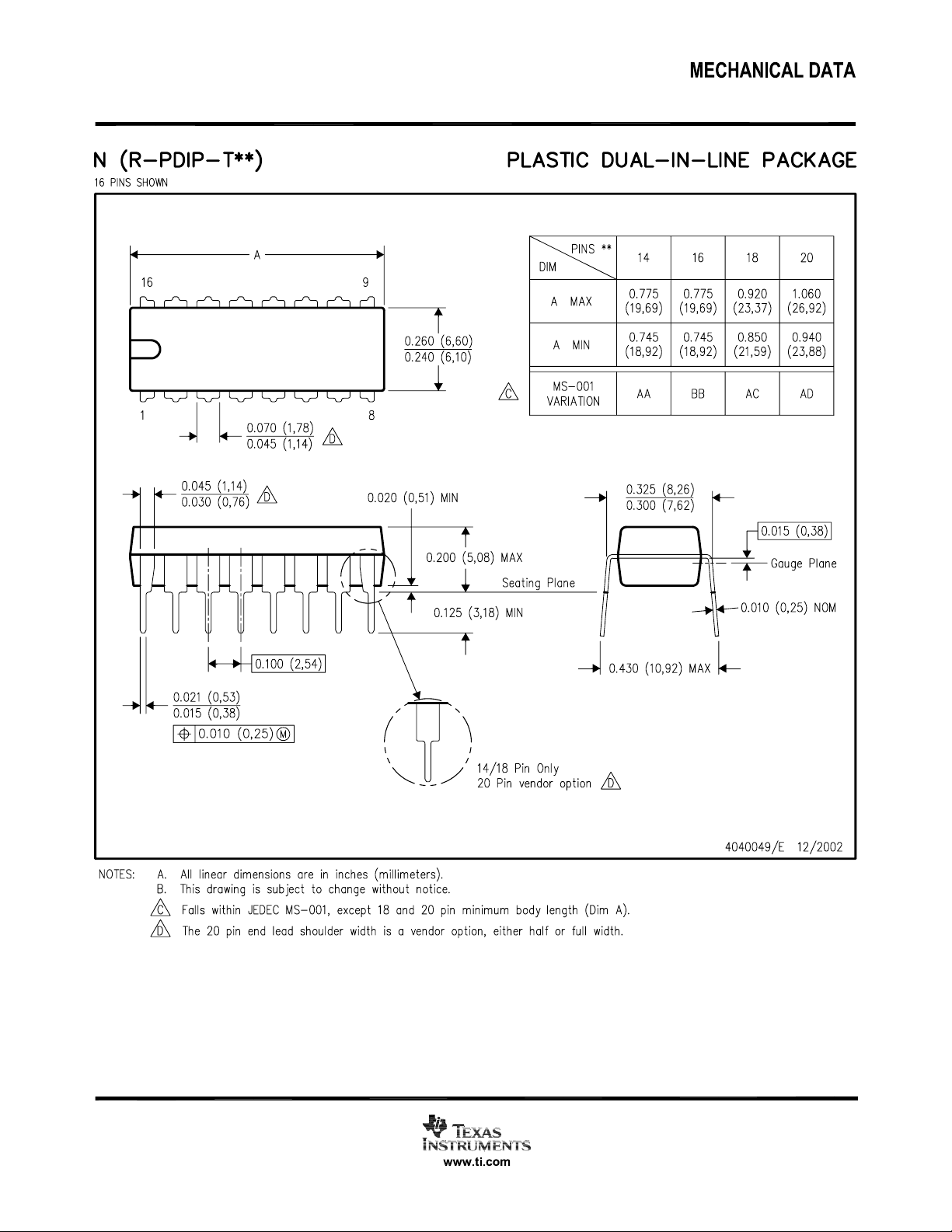
MECHANICAL DATA
MLCC006B – OCTOBER 1996
FK (S-CQCC-N**) LEADLESS CERAMIC CHIP CARRIER
28 TERMINAL SHOWN
A SQ
B SQ
19
20
21
22
23
24
25
12826 27
12
1314151618 17
0.020 (0,51)
0.010 (0,25)
MIN
0.342
(8,69)
0.442
0.640
0.739
0.938
1.141
A
0.358
(9,09)
0.458
(11,63)
0.660
(16,76)
0.761
(19,32)(18,78)
0.962
(24,43)
1.165
(29,59)
NO. OF
TERMINALS
**
11
10
9
8
7
6
5
432
20
28
44
52
68
84
0.020 (0,51)
0.010 (0,25)
(11,23)
(16,26)
(23,83)
(28,99)
MINMAX
0.307
(7,80)
0.406
(10,31)
0.495
(12,58)
0.495
(12,58)
0.850
(21,6)
1.047
(26,6)
0.080 (2,03)
0.064 (1,63)
B
MAX
0.358
(9,09)
0.458
(11,63)
0.560
(14,22)
0.560
(14,22)
0.858
(21,8)
1.063
(27,0)
0.055 (1,40)
0.045 (1,14)
0.028 (0,71)
0.022 (0,54)
0.050 (1,27)
NOTES: A. All linear dimensions are in inches (millimeters).
B. This drawing is subject to change without notice.
C. This package can be hermetically sealed with a metal lid.
D. The terminals are gold plated.
E. Falls within JEDEC MS-004
POST OFFICE BOX 655303 • DALLAS, TEXAS 75265
0.045 (1,14)
0.035 (0,89)
0.045 (1,14)
0.035 (0,89)
4040140/D 10/96
Page 10
Page 11

Page 12

Page 13

MECHANICAL DATA
MSSO002E – JANUARY 1995 – REVISED DECEMBER 2001
DB (R-PDSO-G**) PLASTIC SMALL-OUTLINE
28 PINS SHOWN
0,65
28
1
2,00 MAX
0,38
0,22
15
14
A
0,05 MIN
0,15
5,60
5,00
M
8,20
7,40
Seating Plane
0,10
0,25
0,09
0°–ā8°
Gage Plane
0,25
0,95
0,55
PINS **
DIM
A MAX
A MIN
NOTES: A. All linear dimensions are in millimeters.
B. This drawing is subject to change without notice.
C. Body dimensions do not include mold flash or protrusion not to exceed 0,15.
D. Falls within JEDEC MO-150
14
6,50
6,50
5,905,90
2016
7,50
6,90
24
8,50
28
10,50
9,907,90
30
10,50
9,90
38
12,90
12,30
4040065 /E 12/01
POST OFFICE BOX 655303 • DALLAS, TEXAS 75265
Page 14

IMPORTANT NOTICE
Texas Instruments Incorporated and its subsidiaries (TI) reserve the right to make corrections, modifications,
enhancements, improvements, and other changes to its products and services at any time and to discontinue
any product or service without notice. Customers should obtain the latest relevant information before placing
orders and should verify that such information is current and complete. All products are sold subject to TI’s terms
and conditions of sale supplied at the time of order acknowledgment.
TI warrants performance of its hardware products to the specifications applicable at the time of sale in
accordance with TI’s standard warranty. Testing and other quality control techniques are used to the extent TI
deems necessary to support this warranty . Except where mandated by government requirements, testing of all
parameters of each product is not necessarily performed.
TI assumes no liability for applications assistance or customer product design. Customers are responsible for
their products and applications using TI components. To minimize the risks associated with customer products
and applications, customers should provide adequate design and operating safeguards.
TI does not warrant or represent that any license, either express or implied, is granted under any TI patent right,
copyright, mask work right, or other TI intellectual property right relating to any combination, machine, or process
in which TI products or services are used. Information published by TI regarding third-party products or services
does not constitute a license from TI to use such products or services or a warranty or endorsement thereof.
Use of such information may require a license from a third party under the patents or other intellectual property
of the third party, or a license from TI under the patents or other intellectual property of TI.
Reproduction of information in TI data books or data sheets is permissible only if reproduction is without
alteration and is accompanied by all associated warranties, conditions, limitations, and notices. Reproduction
of this information with alteration is an unfair and deceptive business practice. TI is not responsible or liable for
such altered documentation.
Resale of TI products or services with statements different from or beyond the parameters stated by TI for that
product or service voids all express and any implied warranties for the associated TI product or service and
is an unfair and deceptive business practice. TI is not responsible or liable for any such statements.
Following are URLs where you can obtain information on other Texas Instruments products and application
solutions:
Products Applications
Amplifiers amplifier.ti.com Audio www.ti.com/audio
Data Converters dataconverter.ti.com Automotive www.ti.com/automotive
DSP dsp.ti.com Broadband www.ti.com/broadband
Interface interface.ti.com Digital Control www.ti.com/digitalcontrol
Logic logic.ti.com Military www.ti.com/military
Power Mgmt power.ti.com Optical Networking www.ti.com/opticalnetwork
Microcontrollers microcontroller.ti.com Security www.ti.com/security
Telephony www.ti.com/telephony
Video & Imaging www.ti.com/video
Wireless www.ti.com/wireless
Mailing Address: Texas Instruments
Post Office Box 655303 Dallas, Texas 75265
Copyright 2005, Texas Instruments Incorporated
Page 15

WWW.ALLDATASHEET.COM
Copyright © Each Manufacturing Company.
All Datasheets cannot be modified without permission.
This datasheet has been download from :
www.AllDataSheet.com
100% Free DataSheet Search Site.
Free Download.
No Register.
Fast Search System.
www.AllDataSheet.com
 Loading...