

SN54F04, SN74F04
HEX INVERTERS
SDFS037A – MARCH 1987 – REVISED OCT OBER 1993
• Package Options Include Plastic
Small-Outline Packages, Ceramic Chip
Carriers, and Standard Plastic and Ceramic
300-mil DIPs
description
These devices contain six independent inverters.
They perform the Boolean function Y = A
The SN54F04 is characterized for operation over
the full military temperature range of –55°C to
125°C. The SN74F04 is characterized for
operation from 0°C to 70°C.
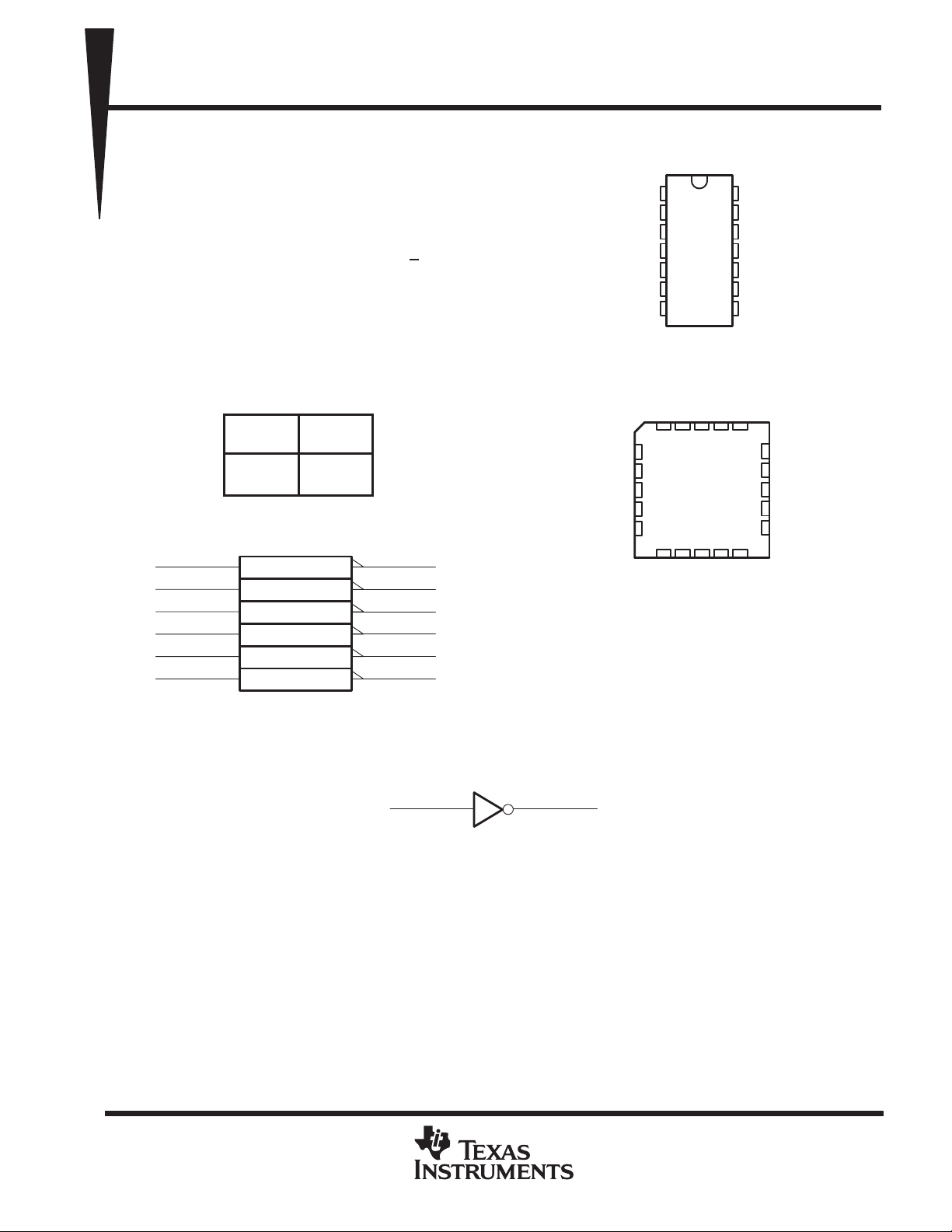
FUNCTION TABLE
(each inverter)
OUTPUT
1
logic symbol
1
1A
3
2A
5
3A
9
4A
11
5A
13
6A
INPUT
A Y
H L
L H
†
10
12
SN54F04 ...J PACKAGE
SN74F04 ...D OR N PACKAGE
.
2A
NC
2Y
NC
3A
2
1Y
4
2Y
6
3Y
8
4Y
5Y
6Y
NC – No internal connection
(TOP VIEW)
1A
1
1Y
2
2A
3
2Y
4
3A
5
3Y
6
GND
SN54F04 . . . FK PACKAGE
7
(TOP VIEW)
1Y1ANC
3212019
4
5
6
7
8
910111213
3Y
GND
14
13
12
11
10
NC
V
CC
6A
6Y
5A
5Y
4A
9
4Y
8
CC
V
6A
18
17
16
15
14
4Y
4A
6Y
NC
5A
NC
5Y
†
This symbol is in accordance with ANSI/IEEE Std 91-1984 and
IEC Publication 617-12.
logic diagram, each inverter (positive logic)
Pin numbers shown are for the D, J, and N packages.
PRODUCTION DATA information is current as of publication date.
Products conform to specifications per the terms of Texas Instruments
standard warranty. Production processing does not necessarily include
testing of all parameters.
YA
Copyright 1993, Texas Instruments Incorporated
POST OFFICE BOX 655303 • DALLAS, TEXAS 75265
2–1
SN54F04, SN74F04
UNIT
PARAMETER
TEST CONDITIONS
UNIT
V
V
HEX INVERTERS
SDFS037A – MARCH 1987 – REVISED OCT OBER 1993
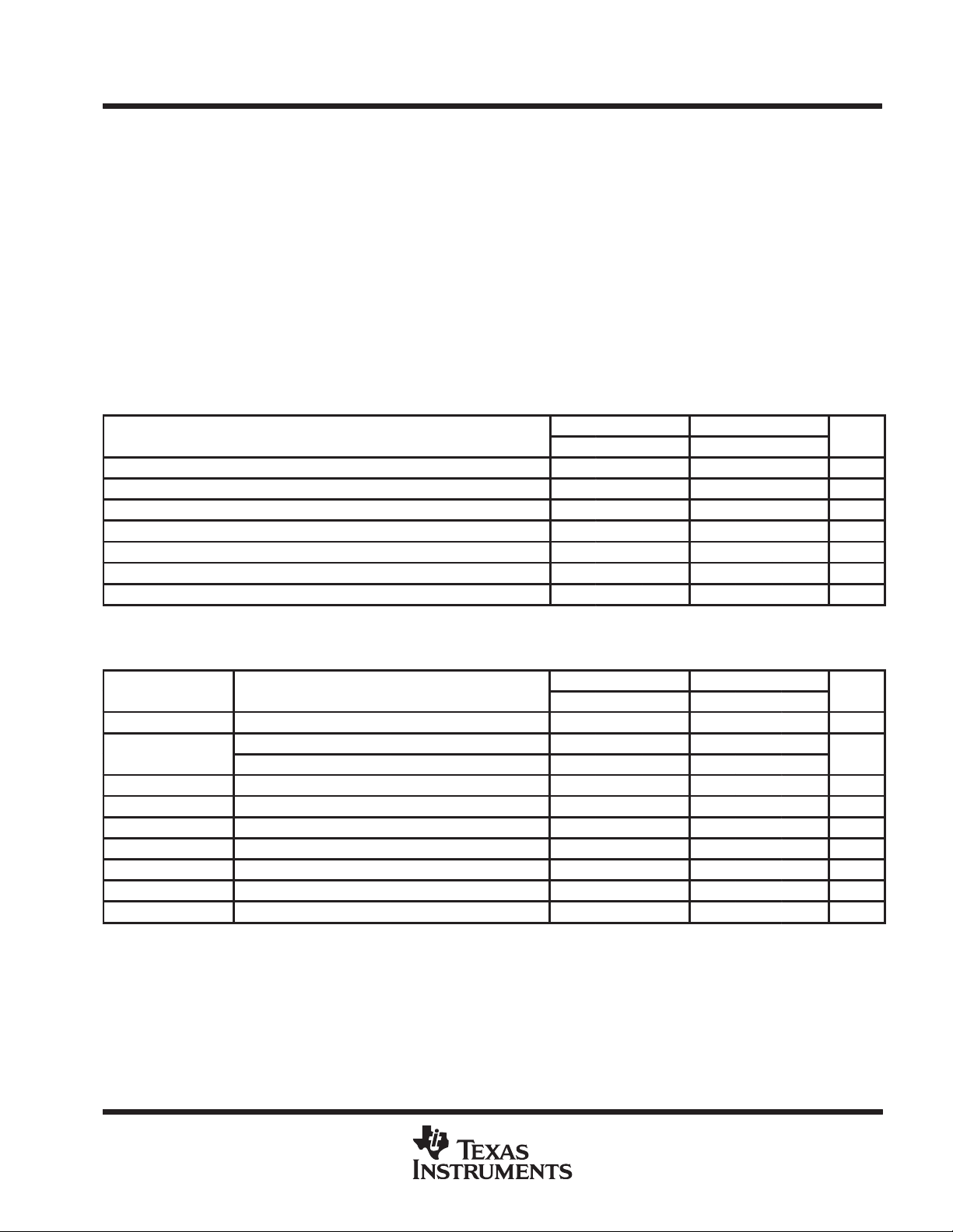
absolute maximum ratings over operating free-air temperature range (unless otherwise noted)
Supply voltage range, V
Input voltage range, V
Input current range –30 mA to 5 mA. . . . . . . . . . . . . . . . . . . . . . . . . . . . . . . . . . . . . . . . . . . . . . . . . . . . . . . . . . . . . .
Voltage range applied to any output in the high state –0.5 V to V
Current into any output in the low state 40 mA. . . . . . . . . . . . . . . . . . . . . . . . . . . . . . . . . . . . . . . . . . . . . . . . . . . . .
Operating free-air temperature range: SN54F04 –55°C to 125°C. . . . . . . . . . . . . . . . . . . . . . . . . . . . . . . . . . . .
Storage temperature range –65°C to 150°C. . . . . . . . . . . . . . . . . . . . . . . . . . . . . . . . . . . . . . . . . . . . . . . . . . . . . . .
†
Stresses beyond those listed under “absolute maximum ratings” may cause permanent damage to the device. These are stress ratings only and
functional operation of the device at these or any other conditions beyond those indicated under “recommended operating conditions” is not
implied. Exposure to absolute-maximum-rated conditions for extended periods may affect device reliability.
NOTE 1: The input voltage ratings may be exceeded provided the input current ratings are observed.
–0.5 V to 7 V. . . . . . . . . . . . . . . . . . . . . . . . . . . . . . . . . . . . . . . . . . . . . . . . . . . . . . . . . .
CC
(see Note 1) –1.2 V to 7 V. . . . . . . . . . . . . . . . . . . . . . . . . . . . . . . . . . . . . . . . . . . . . . . . . .
I
. . . . . . . . . . . . . . . . . . . . . . . . . . . . . . . . . .
SN74F04 0°C to 70°C. . . . . . . . . . . . . . . . . . . . . . . . . . . . . . . . . . . . . . . .
recommended operating conditions
SN54F04 SN74F04
MIN NOM MAX MIN NOM MAX
V
V
V
I
I
I
T
CC
IH
IL
IK
OH
OL
A
Supply voltage 4.5 5 5.5 4.5 5 5.5 V
High-level input voltage 2 2 V
Low-level input voltage 0.8 0.8 V
Input clamp current –18 –18 mA
High-level output current –1 –1 mA
Low-level output current 20 20 mA
Operating free-air temperature –55 125 0 70 °C
†
CC
electrical characteristics over recommended operating free-air temperature range (unless
otherwise noted)
SN54F04 SN74F04
MIN TYP‡MAX MIN TYP‡MAX
V
IK
OH
V
OL
I
I
I
IH
I
IL
§
I
OS
I
CCH
I
‡
§
CCL
All typical values are at VCC = 5 V, TA = 25°C.
Not more than one output should be shorted at a time, and the duration of the short circuit should not exceed one second.
VCC = 4.5 V, II = –18 mA –1.2 –1.2 V
VCC = 4.5 V, IOH = – 1 mA 2.5 3.4 2.5 3.4
VCC = 4.75 V, IOH = – 1 mA 2.7
VCC = 4.5 V, IOL = 20 mA 0.3 0.5 0.3 0.5 V
VCC = 5.5 V, VI = 7 V 0.1 0.1 mA
VCC = 5.5 V, VI = 2.7 V 20 20 µA
VCC = 5.5 V, VI = 0.5 V – 0.6 – 0.6 mA
VCC = 5.5 V, VO = 0 –60 –150 –60 –150 mA
VCC = 5.5 V, VI = 0 2.8 4.2 2.8 4.2 mA
VCC = 5.5 V, VI = 4.5 V 10.2 15.3 10.2 15.3 mA
2–2
POST OFFICE BOX 655303 • DALLAS, TEXAS 75265
SN54F04, SN74F04
(
)
(
)
(INPUT)
(OUTPUT)
A
Y
ns
SDFS037A – MARCH 1987 – REVISED OCTOBER 1993
switching characteristics (see Note 2)
VCC = 5 V,
CL = 50 pF,
PARAMETER
t
PLH
t
†
NOTE 2: Load circuits and waveforms are shown in Section 1.
PHL
For conditions shown as MIN or MAX, use the appropriate value specified under recommended operating conditions.
FROM
INPUT
TO
OUTPUT
RL = 500 Ω,
TA = 25°C
′F04 SN54F04 SN74F04
MIN TYP MAX MIN MAX MIN MAX
1.6 3.3 5 1.2 7 1.6 6
1 2.8 4.3 1 6.5 1 5.3
VCC = 4.5 V to 5.5 V,
CL = 50 pF,
RL = 500Ω,
TA = MIN to MAX
HEX INVERTERS
†
UNIT
POST OFFICE BOX 655303 • DALLAS, TEXAS 75265
2–3

SN54F04, SN74F04
HEX INVERTERS
SDFS037A – MARCH 1987 – REVISED OCT OBER 1993
2–4
POST OFFICE BOX 655303 • DALLAS, TEXAS 75265

PACKAGE OPTION ADDENDUM
www.ti.com
28-Feb-2005
PACKAGING INFORMATION
Orderable Device Status
(1)
Package
Type
Package
Drawing
Pins Package
Qty
Eco Plan
5962-9759301Q2A ACTIVE LCCC FK 20 1 None Call TI Level-NC-NC-NC
5962-9759301QCA ACTIVE CDIP J 14 1 None CallTI Level-NC-NC-NC
5962-9759301QDA ACTIVE CFP W 14 1 None Call TI Level-NC-NC-NC
JM38510/33002B2A ACTIVE LCCC FK 20 1 None Call TI Level-NC-NC-NC
JM38510/33002BCA ACTIVE CDIP J 14 1 None CallTI Level-NC-NC-NC
JM38510/33002BDA ACTIVE CFP W 14 1 None Call TI Level-NC-NC-NC
SN54F04J ACTIVE CDIP J 14 1 None Call TI Level-NC-NC-NC
SN74F04D ACTIVE SOIC D 14 50 Pb-Free
SN74F04DR ACTIVE SOIC D 14 2500 Pb-Free
SN74F04N ACTIVE PDIP N 14 25 Pb-Free
SN74F04N3 OBSOLETE PDIP N 14 None Call TI Call TI
SN74F04NSR ACTIVE SO NS 14 2000 Pb-Free
SNJ54F04FK ACTIVE LCCC FK 20 1 None Call TI Level-NC-NC-NC
SNJ54F04J ACTIVE CDIP J 14 1 None Call TI Level-NC-NC-NC
SNJ54F04W ACTIVE CFP W 14 1 None Call TI Level-NC-NC-NC
(1)
The marketing status values are defined as follows:
ACTIVE: Product device recommended for new designs.
LIFEBUY: TI has announced that the device will be discontinued, and a lifetime-buy period is in effect.
NRND: Not recommended for new designs. Device is in production to support existing customers, but TI does not recommend using this part in
a new design.
PREVIEW: Device has been announced but is not in production. Samples may or may not be available.
OBSOLETE: TI has discontinued the production of the device.
(RoHS)
(RoHS)
(RoHS)
(RoHS)
(2)
Lead/Ball Finish MSL Peak Temp
CU NIPDAU Level-2-260C-1 YEAR/
Level-1-235C-UNLIM
CU NIPDAU Level-2-260C-1 YEAR/
Level-1-235C-UNLIM
CU NIPDAU Level-NC-NC-NC
CU NIPDAU Level-2-260C-1 YEAR/
Level-1-235C-UNLIM
(3)
(2)
Eco Plan - May not be currently available - please check http://www.ti.com/productcontent for the latest availability information and additional
product content details.
None: Not yet available Lead (Pb-Free).
Pb-Free (RoHS): TI's terms "Lead-Free" or "Pb-Free" mean semiconductor products that are compatible with the current RoHS requirements
for all 6 substances, including the requirement that lead not exceed 0.1% by weight in homogeneous materials. Where designed to be soldered
at high temperatures, TI Pb-Free products are suitable for use in specified lead-free processes.
Green (RoHS & no Sb/Br): TI defines "Green" to mean "Pb-Free" and in addition, uses package materials that do not contain halogens,
including bromine (Br) or antimony (Sb) above 0.1% of total product weight.
(3)
MSL, Peak Temp. -- The Moisture Sensitivity Level rating according to the JEDECindustry standard classifications, and peak solder
temperature.
Important Information and Disclaimer:The information provided on this page represents TI's knowledge and belief as of the date that it is
provided. TI bases its knowledge and belief on information provided by third parties, and makes no representation or warranty as to the
accuracy of such information. Efforts are underway to better integrate information from third parties. TI has taken and continues to take
reasonable steps to provide representative and accurate information but may not have conducted destructive testing or chemical analysis on
incoming materials and chemicals. TI and TI suppliers consider certain information to be proprietary, and thus CAS numbers and other limited
information may not be available for release.
In no event shall TI's liability arising out of such information exceed the total purchase price of the TI part(s) at issue in this document sold by TI
to Customer on an annual basis.
Addendum-Page 1

IMPORTANT NOTICE
Texas Instruments Incorporated and its subsidiaries (TI) reserve the right to make corrections, modifications,
enhancements, improvements, and other changes to its products and services at any time and to discontinue
any product or service without notice. Customers should obtain the latest relevant information before placing
orders and should verify that such information is current and complete. All products are sold subject to TI’s terms
and conditions of sale supplied at the time of order acknowledgment.
TI warrants performance of its hardware products to the specifications applicable at the time of sale in
accordance with TI’s standard warranty. Testing and other quality control techniques are used to the extent TI
deems necessary to support this warranty . Except where mandated by government requirements, testing of all
parameters of each product is not necessarily performed.
TI assumes no liability for applications assistance or customer product design. Customers are responsible for
their products and applications using TI components. To minimize the risks associated with customer products
and applications, customers should provide adequate design and operating safeguards.
TI does not warrant or represent that any license, either express or implied, is granted under any TI patent right,
copyright, mask work right, or other TI intellectual property right relating to any combination, machine, or process
in which TI products or services are used. Information published by TI regarding third-party products or services
does not constitute a license from TI to use such products or services or a warranty or endorsement thereof.
Use of such information may require a license from a third party under the patents or other intellectual property
of the third party, or a license from TI under the patents or other intellectual property of TI.
Reproduction of information in TI data books or data sheets is permissible only if reproduction is without
alteration and is accompanied by all associated warranties, conditions, limitations, and notices. Reproduction
of this information with alteration is an unfair and deceptive business practice. TI is not responsible or liable for
such altered documentation.
Resale of TI products or services with statements different from or beyond the parameters stated by TI for that
product or service voids all express and any implied warranties for the associated TI product or service and
is an unfair and deceptive business practice. TI is not responsible or liable for any such statements.
Following are URLs where you can obtain information on other Texas Instruments products and application
solutions:
Products Applications
Amplifiers amplifier.ti.com Audio www.ti.com/audio
Data Converters dataconverter.ti.com Automotive www.ti.com/automotive
DSP dsp.ti.com Broadband www.ti.com/broadband
Interface interface.ti.com Digital Control www.ti.com/digitalcontrol
Logic logic.ti.com Military www.ti.com/military
Power Mgmt power.ti.com Optical Networking www.ti.com/opticalnetwork
Microcontrollers microcontroller.ti.com Security www.ti.com/security
Telephony www.ti.com/telephony
Video & Imaging www.ti.com/video
Wireless www.ti.com/wireless
Mailing Address: Texas Instruments
Post Office Box 655303 Dallas, Texas 75265
Copyright 2005, Texas Instruments Incorporated

WWW.ALLDATASHEET.COM
Copyright © Each Manufacturing Company.
All Datasheets cannot be modified without permission.
This datasheet has been download from :
www.AllDataSheet.com
100% Free DataSheet Search Site.
Free Download.
No Register.
Fast Search System.
www.AllDataSheet.com
 Loading...