

Datasheet SN54AS885JT, SN74AS885DW, SN74AS885DWR, SN74AS885NT, SN74AS885NT3 Datasheet (Texas Instruments)
...Page 1
SN54AS885, SN74AS885
8-BIT MAGNITUDE COMPARATORS
SDAS236A – DECEMBER 1982 – REVISED JANUARY 1995
• Latchable P-Input Ports With Power-Up
Clear
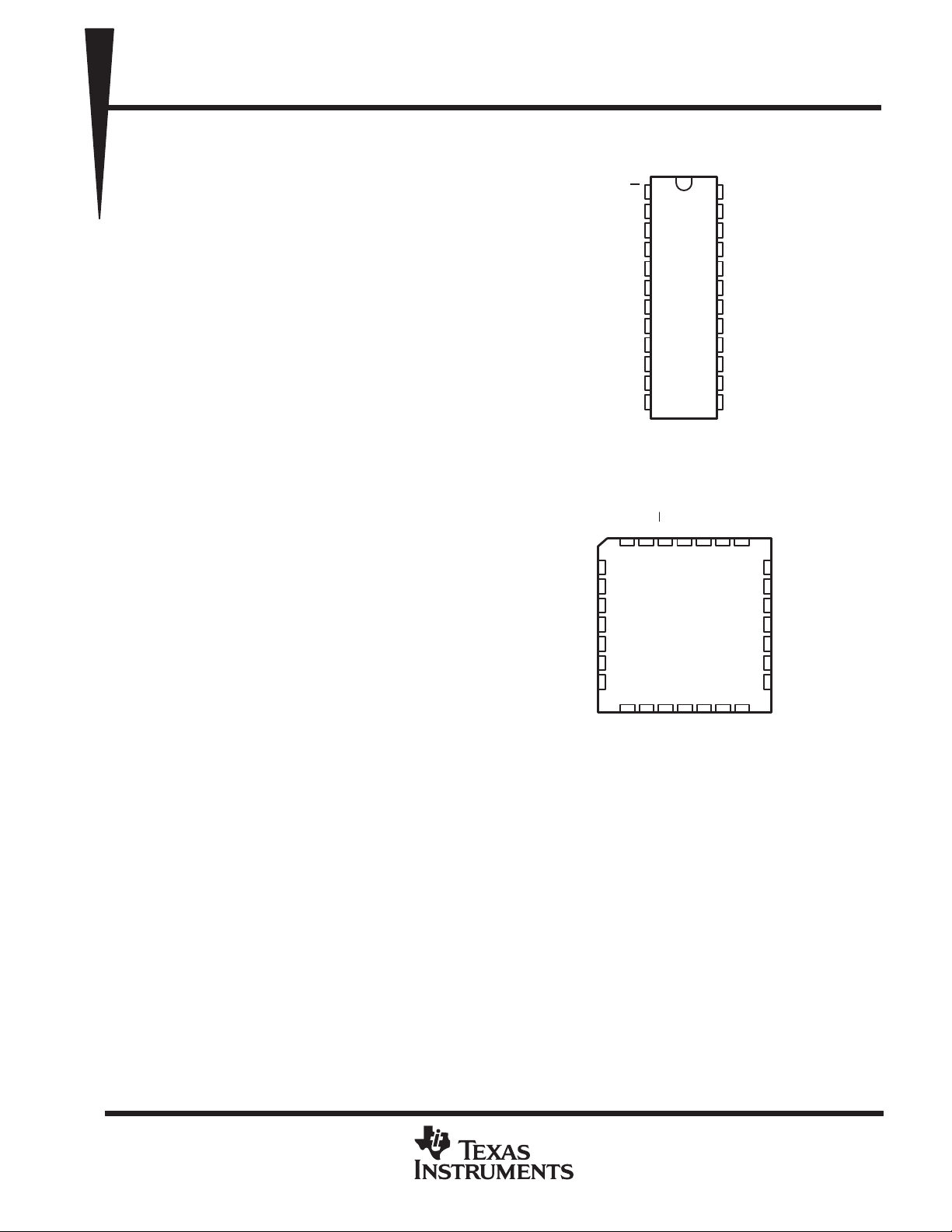
SN54AS885 . . . JT PACKAGE
SN74AS885 . . . DW OR NT PACKAGE
(TOP VIEW)
• Choice of Logical or Arithmetic
(T wo’s Complement) Comparison
• Data and PLE Inputs Utilize pnp Input
Transistors to Reduce dc Loading Effects
• Approximately 35% Improvement in
ac Performance Over Schottky TTL While
Performing More Functions
• Cascadable to n Bits While Maintaining
High Performance
• 10% Less Power Than STTL for an 8-Bit
Comparison
• Package Options Include Plastic
Small-Outline (DW) Packages, Ceramic
Chip Carriers (FK), and Standard Plastic
(NT) and Ceramic (JT) 300-mil DIPs
description
These advanced Schottky devices are capable of
performing high-speed arithmetic or logic
comparisons on two 8-bit binary or two’s
complement words. Two fully decoded decisions
about words P and Q are externally available at
two outputs. These devices are fully expandable
to any number of bits without external gates. To
compare words of longer lengths, the P > QOUT
and P < QOUT outputs of a stage handling less
significant bits can be connected to the P > QIN
and P < QIN inputs of the next stage handling
more significant bits. The cascading paths are
implemented with only a two-gate-level delay to
reduce overall comparison times for long words.
Two alternative methods of cascading are shown
in
application information
.
The latch is transparent when P latch-enable
(PLE) input is high; the P-input port is latched
when PLE is low. This provides the designer with temporary storage for the P-data word. The enable circuitry
is implemented with minimal delay times to enhance performance when cascaded for longer words. The PLE,
P, and Q data inputs utilize pnp input transistors to reduce the low-level current input requirement to typically
–0.25 mA, which minimizes dc loading effects.
L/A
1
24
P < QIN
P > QIN
SN54AS885 . . . FK PACKAGE
Q7
Q6
Q5
NC
Q4
Q3
Q2
NC – No internal connection
2
23
3
22
Q7
4
21
Q6
5
20
Q5
6
19
Q4
7
18
Q3
8
17
Q2
9
16
Q1
10
15
Q0
11
14
GND
12
13
(TOP VIEW)
P > QIN
P < QIN
L/A
NC
V
3212827
426
5
6
7
8
9
10
11
12 13
14 15 16 17 18
Q1
Q0
NC
GND
P > QOUT
V
CC
PLE
P7
P6
P5
P4
P3
P2
P1
P0
P < QOUT
P > QOUT
CC
PLE
P7
25
24
23
22
21
20
19
P0
P < QOUT
P6
P5
P4
NC
P3
P2
P1
The SN54AS885 is characterized for operation over the full military temperature range of –55°C to 125°C. The
SN74AS885 is characterized for operation from 0°C to 70°C.
PRODUCTION DATA information is current as of publication date.
Products conform to specifications per the terms of Texas Instruments
standard warranty. Production processing does not necessarily include
testing of all parameters.
POST OFFICE BOX 655303 • DALLAS, TEXAS 75265
Copyright 1995, Texas Instruments Incorporated
1
Page 2
SN54AS885, SN74AS885
8-BIT MAGNITUDE COMPARATORS
SDAS236A – DECEMBER 1982 – REVISED JANUAR Y 1995
COMPARISON
Logical H P > Q X X H L
Logical H P < Q X XL H
†
Logical
Arithmetic L P AG Q X XH L
Arithmetic L Q AG P X XL H
Arithmetic
†
In these cases, P > QOUT follows P > QIN and P < QOUT follows P < QIN.
AG = arithmetically greater than
L/A
H P = Q H or L H or L H or L H or L
†
L P = Q H or L H or L H or L H or L
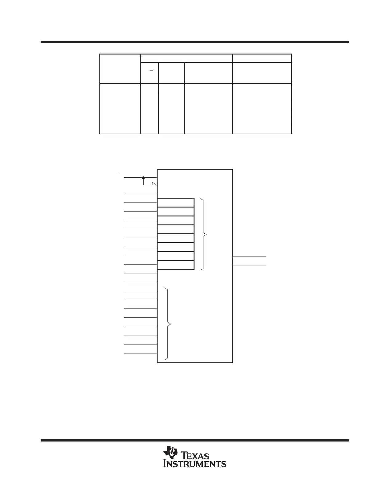
FUNCTION TABLE
INPUTS OUTPUTS
DATA
P0–P7,
Q0–Q7
P > QIN P < QIN P > QOUT P < QOUT
logic symbol
‡
L/A
PLE
P0
P1
P2
P3
P4
P5
P6
P7
P > QIN
P < QIN
Q0
Q1
Q2
Q3
Q4
Q5
Q6
Q7
1
23
15
16
17
18
19
20
21
22
3
2
11
10
9
8
7
6
5
4
M [LOGIC]
M [ARITH, 2s COMP]
C1
1D
>
<
0
7
Q
COMP
1=0 0
P
13
P > Q
7
P < Q
14
P > QOUT
P < QOUT
‡
This symbol is in accordance with ANSI/IEEE Std 91-1984 and IEC Publication 617-12.
Pin numbers shown are for the DW, JT, and NT packages.
2
POST OFFICE BOX 655303 • DALLAS, TEXAS 75265
Page 3
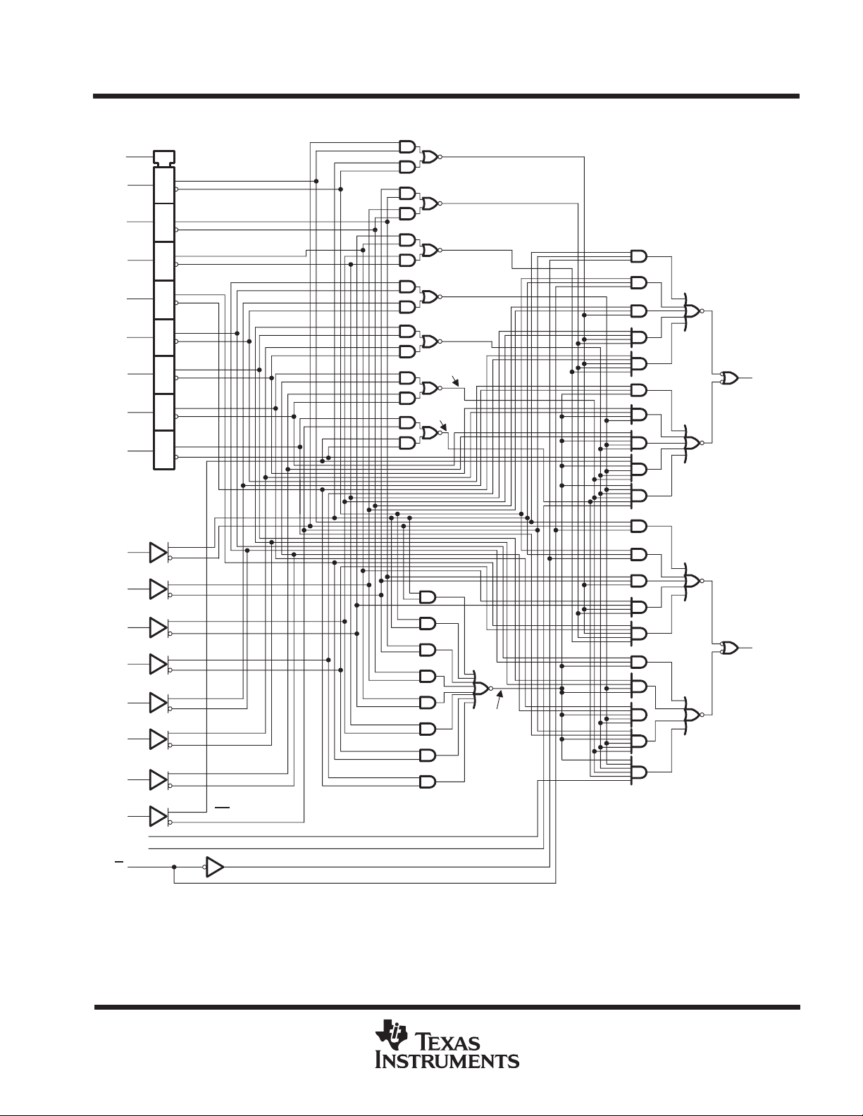
logic diagram (positive logic)
SN54AS885, SN74AS885
8-BIT MAGNITUDE COMPARATORS
SDAS236A – DECEMBER 1982 – REVISED JANUARY 1995
PLE
P7
P6
P5
P4
P3
P2
P1
P0
Q7
Q6
Q5
Q4
Q3
Q2
Q1
Q0
P > QIN
P < QIN
L/A
23
22
21
20
19
18
17
16
15
4
5
6
7
8
9
10
11
1
C1
3
2
1D
Q7
Q7
Q6
Q6
Q5
Q5
Q4
Q4
Q3
Q3
Q2
Q2
Q1
Q1
Q0
P7
P7
P6
P6
P5
P5
P4
P4
P3
P3
P2
P2
P1
P1
P0
P0
Q0
ARITH
LOGIC
P2 = Q2
P1 = Q1
P0 = Q0
P7 = Q7
P6 = Q6
P5 = Q5
P3 = Q3
14
P < QOUT
13
P > QOUT
4MSB =
Pin numbers shown are for the DW, JT, and NT packages.
POST OFFICE BOX 655303 • DALLAS, TEXAS 75265
3
Page 4

SN54AS885, SN74AS885
UNIT
PARAMETER
TEST CONDITIONS
UNIT
I
V
V
V
A
8-BIT MAGNITUDE COMPARATORS
SDAS236A – DECEMBER 1982 – REVISED JANUAR Y 1995
absolute maximum ratings over operating free-air temperature range (unless otherwise noted)
Supply voltage, V
Input voltage, V
Operating free-air temperature range, T
Storage temperature range –65°C to 150°C. . . . . . . . . . . . . . . . . . . . . . . . . . . . . . . . . . . . . . . . . . . . . . . . . . . . . . .
†
Stresses beyond those listed under “absolute maximum ratings” may cause permanent damage to the device. These are stress ratings only, and
functional operation of the device at these or any other conditions beyond those indicated under “recommended operating conditions” is not
implied. Exposure to absolute-maximum-rated conditions for extended periods may affect device reliability.
7 V. . . . . . . . . . . . . . . . . . . . . . . . . . . . . . . . . . . . . . . . . . . . . . . . . . . . . . . . . . . . . . . . . . . . . . . .
CC
7 V. . . . . . . . . . . . . . . . . . . . . . . . . . . . . . . . . . . . . . . . . . . . . . . . . . . . . . . . . . . . . . . . . . . . . . . . . . . .
I
: SN54AS885 –55°C to 125°C. . . . . . . . . . . . . . . . . . . . . . . . . . . . . .
A
SN74AS885 0°C to 70°C. . . . . . . . . . . . . . . . . . . . . . . . . . . . . . . . . .
recommended operating conditions
SN54AS885 SN74AS885
MIN NOM MAX MIN NOM MAX
V
CC
V
IH
V
IL
I
OH
I
OL
tsu* Setup time, data before PLE↓ 2 2 ns
th* Hold time, data after PLE↓ 4.5 4 ns
T
A
* On products compliant to MIL-STD-883, Class B, this parameter is based on characterization data but is not production tested.
Supply voltage 4.5 5 5.5 4.5 5 5.5 V
High-level input voltage 2 2 V
Low-level input voltage 0.8 0.8 V
High-level output current –2 –2 mA
Low-level output current 20 20 mA
Operating free-air temperature –55 125 0 70 °C
†
electrical characteristics over recommended operating free-air temperature range (unless
otherwise noted)
SN54AS885 SN74AS885
MIN TYP‡MAX MIN TYP‡MAX
V
IK
V
OH
V
OL
I
I
IH
I
IL
I
O
I
CC
‡
All typical values are at VCC = 5 V, TA = 25°C.
§
The output conditions have been chosen to produce a current that closely approximates one half of the true short-circuit output current, IOS.
NOTE 1: ICC is measured with all inputs high except L/A
L/A
Others
L/A –4 –4
P > QIN, P < QIN
P, Q, PLE –1 –1
§
VCC = 4.5 V, II = –18 mA –1.2 –1.2 V
VCC = 4.5 V to 5.5 V, IOH = –2 mA VCC –2 VCC –2 V
VCC = 4.5 V, IOL = 20 mA 0.35 0.5 0.35 0.5 V
VCC = 5.5 V, VI = 7 V 0.1 0.1 mA
= 5.5 V,
CC
VCC = 5.5 V, VI = 0.4 V
VCC = 5.5 V, VO = 2.25 V –20 –112 –20 –112 mA
VCC = 5.5 V, See Note 1 130 210 130 210 mA
= 2.7
I
, which is low.
40 40
20 20
–2 –2
µ
mA
4
POST OFFICE BOX 655303 • DALLAS, TEXAS 75265
Page 5

switching characteristics (see Figure 3)
(
)
(
)
(INPUT)
(OUTPUT)
L/A
Q,
ns
,
Q,
ns
y
Q,
ns
PARAMETER
t
PLH
t
PHL
t
PLH
t
PHL
t
PLH
t
†
All typical values are at VCC = 5 V, TA = 25°C.
PHL
FROM
INPUT
P < QIN,
P > QIN
Any P or Q
data input
APPLICATION INFORMATION
TO
OUTPUT
P < QOUT,
P > QOUT
P < QOUT,
P > QOUT
P < QOUT,
P > QOUT
SN54AS885, SN74AS885
8-BIT MAGNITUDE COMPARATORS
SDAS236A – DECEMBER 1982 – REVISED JANUARY 1995
VCC = 4.5 V to 5.5 V,
CL = 50 pF,
RL = 500 Ω
TA = MIN to MAX
SN54AS885 SN74AS885
MIN TYP†MAX MIN TYP†MAX
2 8.5 14 1 8.5 13
2 7.5 14 1 7.5 13
2 5 10 1 5 8
2 5.5 10 1 5.5 8
2 13.5 21 1 13.5 17.5
2 10 17 1 10 15
,
UNIT
The ′AS885 can be cascaded to compare words longer than eight bits. Figure 1 shows the comparison of two 32-bit
words; however, the design is expandable to n bits. Figure 1 shows the optimum cascading arrangement for
comparing words of 32 bits or greater. Typical delay times shown are at V
advanced Schottky load of R
= 500 Ω, CL = 50 pF.
L
= 5 V , TA = 25°C and use the standard
CC
Figure 2 shows the fastest cascading arrangement for comparing 16-bit or 24-bit words. Typical delay times shown
are at V
= 5 V, TA = 25°C and use the standard advanced Schottky load of RL = 500 Ω, CL= 50 pF.
CC
POST OFFICE BOX 655303 • DALLAS, TEXAS 75265
5
Page 6

SN54AS885, SN74AS885
8-BIT MAGNITUDE COMPARATORS
SDAS236A – DECEMBER 1982 – REVISED JANUAR Y 1995
APPLICATION INFORMATION
PLE
H or L
H or L
H or L
H or L
L/A
PLE
P > QIN
P < QIN
L/A
PLE
P > QIN
P < QIN
P0
P1
P2
P3
P4
P5
P6
P7
Q0
Q1
Q2
Q3
Q4
Q5
Q6
Q7
P0
P1
P2
P3
P4
P5
P6
P7
Q0
Q1
Q2
Q3
Q4
Q5
Q6
Q7
1
23
15
16
17
18
19
20
21
22
3
2
11
10
9
8
7
6
5
4
1
23
15
16
17
18
19
20
21
22
3
2
11
10
9
8
7
6
5
4
′AS885
P > QOUT
P < QOUT
′AS885
P > QOUT
P < QOUT
13
14
1
L/A
23
PLE
15
P0
16
P1
17
P2
18
P3
19
P4
20
P5
21
P6
22
P7
3
P > QIN
2
P < QIN
11
Q0
10
Q1
9
Q2
8
Q3
7
Q4
6
Q5
5
Q6
4
Q7
13
14
1
L/A
23
PLE
15
P0
16
P1
17
P2
18
P3
19
P4
20
P5
21
P6
22
P7
3
P > QIN
2
P < QIN
11
Q0
10
Q1
9
Q2
8
Q3
7
Q4
6
Q5
5
Q6
4
Q7
′AS885
P > QOUT
P < QOUT
H or L
′AS885
P > QOUT
P < QOUT
13
14
13
14
L/A
PLE
P > QIN
P < QIN
P0
P1
P2
P3
P4
P5
P6
P7
Q0
Q1
Q2
Q3
Q4
Q5
Q6
Q7
1
23
15
16
17
18
19
20
21
22
3
2
11
10
9
8
7
6
5
4
′AS885
P > QOUT
P < QOUT
PLE
13
P > QOUT
14
P < QOUT
13.5 ns
Typical
13.5 ns
Typical
Figure 1. 32-Bit to 72 (n)-Bit Magnitude Comparator
6
POST OFFICE BOX 655303 • DALLAS, TEXAS 75265
Page 7

Latch
Enable
SN54AS885, SN74AS885
8-BIT MAGNITUDE COMPARATORS
SDAS236A – DECEMBER 1982 – REVISED JANUARY 1995
APPLICATION INFORMATION
H or L
LSB
L/A
PLE
P0
P1
P2
P3
P4
P5
P6
P7
P > QIN
P < QIN
Q0
Q1
Q2
Q3
Q4
Q5
Q6
Q7
1
23
15
16
17
18
19
20
21
22
3
2
11
10
9
8
7
6
5
4
′AS885
P > QOUT
P < QOUT
LSP MSP
13
14
16 Bit
19 ns
Typical
P > QIN
P < QIN
L/A
PLE
P0
P1
P2
P3
P4
P5
P6
P7
Q0
Q1
Q2
Q3
Q4
Q5
Q6
Q7
1
23
15
16
17
18
19
20
21
22
3
2
11
10
9
8
7
6
5
4
′AS885
P > QOUT
P < QOUT
13
MSB
14
24 Bit
24.4 ns
Typical
P > QIN
P < QIN
MSB
L/A
PLE
P0
P1
P2
P3
P4
P5
P6
P7
Q0
Q1
Q2
Q3
Q4
Q5
Q6
Q7
1
23
15
16
17
18
19
20
21
22
3
2
11
10
9
8
7
6
5
4
′AS885
P > QOUT
P < QOUT
13
14
Figure 2. Fastest Cascading Arrangement for Comparing 16-Bit or 24-Bit Words
POST OFFICE BOX 655303 • DALLAS, TEXAS 75265
7
Page 8

SN54AS885, SN74AS885
8-BIT MAGNITUDE COMPARATORS
SDAS236A – DECEMBER 1982 – REVISED JANUAR Y 1995
PARAMETER MEASUREMENT INFORMATION
SERIES 54ALS/74ALS AND 54AS/74AS DEVICES
From Output
Under Test
(see Note A)
C
L
Test
Point
R
L
From Output
Under Test
C
(see Note A)
7 V
V
CC
S1
R
L
Test
Point
L
From Output
Under Test
(see Note A)
R1
C
L
RL = R1 = R2
Test
Point
R2
LOAD CIRCUIT FOR
BI-STATE
TOTEM-POLE OUTPUTS
Timing
Input
t
su
Data
Input
VOLTAGE WAVEFORMS
SETUP AND HOLD TIMES
Output
Control
(low-level
enabling)
Waveform 1
S1 Closed
(see Note B)
Waveform 2
S1 Open
(see Note B)
t
PZL
t
PZH
ENABLE AND DISABLE TIMES, 3-STATE OUTPUTS
VOLTAGE WAVEFORMS
1.3 V
t
PHZ
1.3 V
1.3 V
t
h
1.3 V1.3 V
1.3 V1.3 V
FOR OPEN-COLLECTOR OUTPUTS
t
PLZ
LOAD CIRCUIT
3.5 V
0.3 V
3.5 V
0.3 V
3.5 V
0.3 V
[
3.5 V
V
OL
0.3 V
V
OH
0.3 V
[
0 V
High-Level
Pulse
Low-Level
Pulse
In-Phase
Out-of-Phase
(see Note C)
FOR 3-STATE OUTPUTS
1.3 V 1.3 V
1.3 V 1.3 V
VOLTAGE WAVEFORMS
PULSE DURATIONS
Input
Output
Output
t
PLH
t
PHL
1.3 V 1.3 V
VOLTAGE WAVEFORMS
PROPAGATION DELAY TIMES
LOAD CIRCUIT
t
w
1.3 V1.3 V
1.3 V 1.3 V
t
PHL
t
PLH
3.5 V
0.3 V
3.5 V
0.3 V
3.5 V
0.3 V
V
V
V
V
OH
OL
OH
OL
NOTES: A. CL includes probe and jig capacitance.
B. Waveform 1 is for an output with internal conditions such that the output is low except when disabled by the output control.
Waveform 2 is for an output with internal conditions such that the output is high except when disabled by the output control.
C. When measuring propagation delay items of 3-state outputs, switch S1 is open.
D. All input pulses have the following characteristics: PRR ≤ 1 MHz, tr = tf = 2 ns, duty cycle = 50%.
E. The outputs are measured one at a time with one transition per measurement.
Figure 3. Load Circuits and Voltage Waveforms
8
POST OFFICE BOX 655303 • DALLAS, TEXAS 75265
Page 9

IMPORTANT NOTICE
T exas Instruments and its subsidiaries (TI) reserve the right to make changes to their products or to discontinue
any product or service without notice, and advise customers to obtain the latest version of relevant information
to verify, before placing orders, that information being relied on is current and complete. All products are sold
subject to the terms and conditions of sale supplied at the time of order acknowledgement, including those
pertaining to warranty, patent infringement, and limitation of liability.
TI warrants performance of its semiconductor products to the specifications applicable at the time of sale in
accordance with TI’s standard warranty. Testing and other quality control techniques are utilized to the extent
TI deems necessary to support this warranty . Specific testing of all parameters of each device is not necessarily
performed, except those mandated by government requirements.
CERT AIN APPLICATIONS USING SEMICONDUCTOR PRODUCTS MAY INVOLVE POTENTIAL RISKS OF
DEATH, PERSONAL INJURY, OR SEVERE PROPERTY OR ENVIRONMENTAL DAMAGE (“CRITICAL
APPLICATIONS”). TI SEMICONDUCTOR PRODUCTS ARE NOT DESIGNED, AUTHORIZED, OR
WARRANTED TO BE SUITABLE FOR USE IN LIFE-SUPPORT DEVICES OR SYSTEMS OR OTHER
CRITICAL APPLICA TIONS. INCLUSION OF TI PRODUCTS IN SUCH APPLICATIONS IS UNDERST OOD TO
BE FULLY AT THE CUSTOMER’S RISK.
In order to minimize risks associated with the customer’s applications, adequate design and operating
safeguards must be provided by the customer to minimize inherent or procedural hazards.
TI assumes no liability for applications assistance or customer product design. TI does not warrant or represent
that any license, either express or implied, is granted under any patent right, copyright, mask work right, or other
intellectual property right of TI covering or relating to any combination, machine, or process in which such
semiconductor products or services might be or are used. TI’s publication of information regarding any third
party’s products or services does not constitute TI’s approval, warranty or endorsement thereof.
Copyright 1998, Texas Instruments Incorporated
 Loading...