

Datasheet SN54AS181BJT, SN74AS181ADW, SN74AS181ADWR, SN74AS181AN, SN74AS181ANT Datasheet (Texas Instruments)
...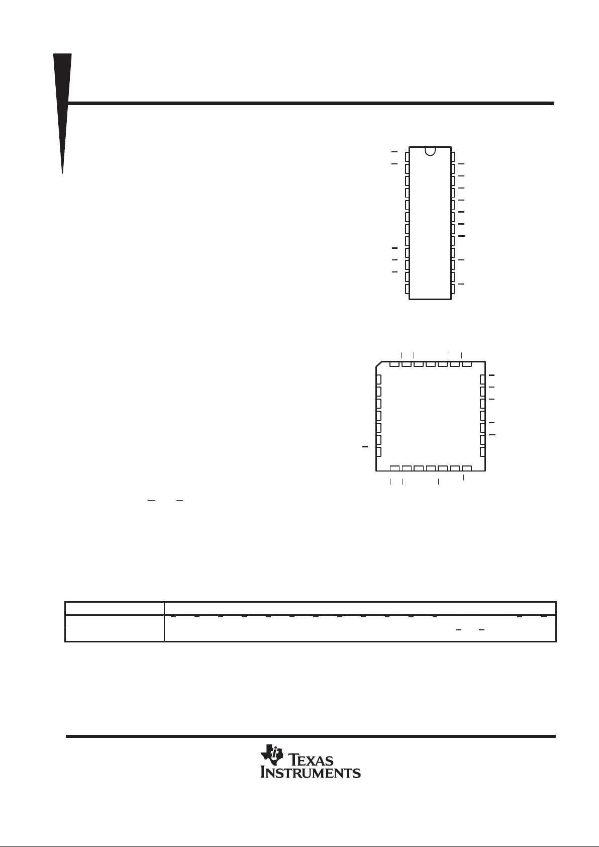
SN54AS181B . . . JT OR JW PACKAGE
SN74AS181A ...N OR NT PACKAGE
(TOP VIEW)
SN54AS181B . . . FK PACKAGE
(TOP VIEW)
1
2
3
4
5
6
7
8
9
10
11
12
24
23
22
21
20
19
18
17
16
15
14
13
B0
A0
S3
S2
S1
S0
C
n
M
F
0
F1
F
2
GND
V
CC
A1
B
1
A
2
B2
A
3
B3
G
C
n + 4
P
A = B
F3
NC – No internal connection
3212827
12 13
5
6
7
8
9
10
11
25
24
23
22
21
20
19
A2
B
2
A
3
NC
B
3
G
C
n + 4
S2
S1
S0
NC
C
n
M
F
0
426
14 15 16 17 18
F1
F2
GND
NC
F3
A = B
P
S3A0B0
NC
A1
B1
V
CC
SN54AS181B, SN74AS181A
ARITHMETIC LOGIC UNITS/FUNCTION GENERATORS
SDAS209B – DECEMBER 1982 – REVISED DECEMBER 1994
Copyright 1994, Texas Instruments Incorporated
1
POST OFFICE BOX 655303 • DALLAS, TEXAS 75265
• Full Look Ahead for High-Speed Operations
on Long Words
• Arithmetic Operating Modes:
– Addition
– Subtraction
– Shift Operand A One Position
– Magnitude Comparison
– Twelve Other Arithmetic Operations
• Logic Function Modes:
– Exclusive-OR
– Comparator
– AND, NAND, OR, NOR
• Package Options Include Plastic
Small-Outline (N) Packages, Ceramic (FK)
Chip Carriers, Standard Plastic (NT) and
Ceramic (JT) 300-mil DIPs, and Ceramic
(JW) 600-mil DIPs
description
The SN54AS181B and SN74AS181A arithmetic
logic units (ALUs)/function generators have a
complexity of 75 equivalent gates on a monolithic
chip. These circuits perform 16 binary arithmetic
operations on two 4-bit words as shown in
T ables1 and 2. These operations are selected by
the four function-select (S0, S1, S2, and S3) lines
and include addition, subtraction, decrement, and
straight transfer. When performing arithmetic
manipulations, the internal carries are enabled by
applying a low-level voltage to the mode-control
(M) input. A full carry look-ahead scheme is used
to generate fast, simultaneous carry by means of
two cascade (G
and P) outputs for the four bits in
the package.
If high speed is not important, a ripple-carry (C
n
) input and a ripple-carry (C
n + 4
) output are available. The
ripple-carry delay is minimized so that arithmetic manipulations for small word lengths can be performed without
external circuitry.
The SN54AS181B and SN74AS181A accommodate active-high or active-low data if the pin designations are
interpreted as follows:
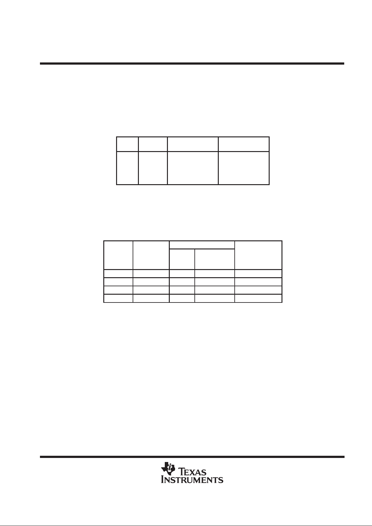
PIN NUMBER 2 1 23 22 21 20 19 18 9 10 11 13 7 16 15 17
Active-low data (Table 1) A0 B0 A1 B1 A2 B2 A3 B3 F0 F1 F2 F3 CnCn + 4P G
Active-high data (Table 2) A0 B0 A1 B1 A2 B2 A3 B3 F0 F1 F2 F3 CnCn + 4X Y
Subtraction is accomplished by 1’s complement addition where the 1’s complement of the subtrahend is
generated internally . The resultant output is A-B-1, which requires an end-around or forced carry to provide A-B.
PRODUCTION DATA information is current as of publication date.
Products conform to specifications per the terms of Texas Instruments
standard warranty. Production processing does not necessarily include
testing of all parameters.
SN54AS181B, SN74AS181A
ARITHMETIC LOGIC UNITS/FUNCTION GENERATORS
SDAS209B – DECEMBER 1982 – REVISED DECEMBER 1994
2
POST OFFICE BOX 655303 • DALLAS, TEXAS 75265
description (continued)
The SN54AS181B and SN74AS181A also can be used as comparators. The A = B output is internally decoded
from the function (F0, F1, F2, F3) outputs so that when two words of equal magnitude are applied at the A and
B inputs, the output assumes a high level to indicate equality (A = B). The ALU must be in the subtract mode
with C
n
= H when performing this comparison. The A = B output is open collector so that it can be wire-AND
connected to give a comparison for more than four bits. C
n + 4
also can be used to supply relative magnitude
information. The ALU must be placed in the subtract mode by placing the function-select inputs S3, S2, S1, and
S0 at L, H, H, and L, respectively.
INPUT
C
n
OUTPUT
Cn +
4
ACTIVE-LOW DATA
(Figure 1)
ACTIVE-HIGH DATA
(Figure 2)
H H A ≥ B A ≤ B
H L A < B A > B
L H A > B A < B
L L A ≤ B A ≥ B
These circuits not only incorporate all of the designer’s requirements for arithmetic operations, but also provide
16 possible functions of two Boolean variables without using external circuitry. These logic functions are
selected by the four function-select inputs with M at a high level to disable the internal carry. The 16 logic
functions are detailed in Tables 1 and 2 and include exclusive-OR, NAND, AND, NOR, and OR functions.
TYPICAL ADDITION TIME
(CL = 15 pF, RL = 280 Ω, TA = 25°C)
ADDITION
PACKAGE COUNT
NUMBER
OF BITS
TIME USING
′S181 AND
′S182
ALUs
LOOK-AHEAD
CARRY
GENERAT ORS
CARRY METHOD
BETWEEN ALUs
1 to 4 11 ns 1 None
5 to 8 18 ns 2 Ripple
9 to 16 19 ns 3 or 4 1 Full look ahead
17 to 64 28 ns 5 to 16 2 to 5 Full look ahead
The SN54AS181B is characterized for operation over the full military temperature range of –55°C to 125°C. The
SN74AS181A is characterized for operation from 0°C to 70°C.
application note
An application-specific problem has been identified in the SN54AS181B device. The F0 –F4 outputs exhibit
voltage transients when one or more B-data inputs transition from a high to a low state. The resultant voltage
transients can have an amplitude of 2 V relative to V
OL
with a width of 5 ns at an input threshold of 1.5 V. The
transient pulse occurs coincidentally with the high-to-low transition of the B-data input(s) and appears to be
caused by internal coupling.
In system operations in which this device is used, it is likely that transmission-line effects minimize this anomaly .
Narrow width of the voltage transient makes the pulse transparent to most circuitry; however, in certain
applications, the transients can cause system errors.
SN54AS181B, SN74AS181A
ARITHMETIC LOGIC UNITS/FUNCTION GENERATORS
SDAS209B – DECEMBER 1982 – REVISED DECEMBER 1994
3
POST OFFICE BOX 655303 • DALLAS, TEXAS 75265
logic symbol
†
M
0
31
0
6
S0
5
S1
4
S2
3
S3
4
8
M
15
A = B
14
C1
7
17
16
9
10
11
13
P
2
Q
1
P
23
Q
22
P
21
Q
20
P
19
Q
18
ALU
[1]
[2]
[3]
[8]
C
n
A
0
A
1
A
2
A3
B
0
B
1
B
2
B3
(0 . . . 15) CP
(0 . . . 15) CG
6(P=Q)
(0 . . . 15) CO
P
G
Cn +
4
F
0
F1
F2
F
3
†
This symbol is in accordance with ANSI/IEEE Std 91-1984 and IEC Publication 617-12.
Pin numbers shown are for the JT, JW, N, and NT packages.
SN54AS181B, SN74AS181A
ARITHMETIC LOGIC UNITS/FUNCTION GENERATORS
SDAS209B – DECEMBER 1982 – REVISED DECEMBER 1994
4
POST OFFICE BOX 655303 • DALLAS, TEXAS 75265
logic diagram
C
n
A
0
A
1
A
2
A
3
B
0
B
1
B
2
B
3
P
G
Cn +
4
F
0
F
1
F
2
F
3
S3
S2
S1
S0
M
3
4
5
6
18
19
20
21
22
23
1
2
8
7
A = B
17
16
15
13
11
14
10
9
Pin numbers shown are for the JT, JW, N, and NT packages.

SN54AS181B, SN74AS181A
ARITHMETIC LOGIC UNITS/FUNCTION GENERATORS
SDAS209B – DECEMBER 1982 – REVISED DECEMBER 1994
5
POST OFFICE BOX 655303 • DALLAS, TEXAS 75265
signal designations
In Figures 1 and 2, the polarity indicators ( ) indicate that the associated input or output is active low with
respect to the function shown inside the symbol. The symbols are the same in both figures. The signal
designations in Figure 1 agree with the indicated internal functions based on active-low data and are for use
with the logic functions and arithmetic operations shown in T able 1. The signal designations have been changed
in Figure 2 to accommodate the logic functions and arithmetic operations for the active-high data given in
T able 2. The SN54AS181B and SN74AS181A together with the ′S182 can be used with the signal designation
of either Figure 1 or Figure 2.
M
0
31
0
6
S0
5
S1
4
S2
3
S3
4
8
M
15
A = B
14
C1
7
17
16
9
10
11
13
P
2
Q
1
P
23
Q
22
P
21
Q
20
P
19
Q
18
ALU
[1]
[2]
[3]
[8]
C
n
A
0
A
1
A2
A
3
B0
B
1
B2
B
3
(0 . . . 15) CP
(0 . . . 15) CG
6(P=Q)
(0 . . . 15) CO
P
G
Cn +
4
F0
F
1
F
2
F
3
SN54AS181B,
SN74AS181A
M
0
31
0
6
S0
5
S1
4
S2
3
S3
4
8
M
15
A = B
14
7
17
16
F0
9
F1
10
F2
11
F3
13
P
2
Q
1
P
23
Q
22
P
21
Q
20
P
19
Q
18
ALU
[1]
[2]
[3]
[8]
C
n
A
0
A
1
A2
A
3
B0
B
1
B2
B
3
(0 . . . 15) CP
(0 . . . 15) CG
6(P=Q)
(0 . . . 15) CO
X
Y
C
n + 4
SN54AS181B,
SN74AS181A
CP0
3
CG0
2
CPG
CP1
5
CG1
4
CP2
8
CG2
7
CP3
10
CG3
9
CP4
14
CG4
13
CP5
16
CG5
15
CP6
19
CG6
18
CP7
21
CG7
20
1
6
CO1
11
CO3
17
CO5
22
CO7
C
n
P
0
G0
P
1
G1
P
2
G2
P3
G3
P4
G4
P5
G5
P
6
G6
P
7
G7
′S182
Cn +
8
Cn +
16
Cn +
24
Cn +
32
C1
CP0
3
CG0
2
CPG
CP1
5
X1
CG1
4
Y1
CP2
8
X2
CG2
7
Y2
CP3
10
X3
CG3
9
Y3
CP4
14
X4
CG4
13
Y4
CP5
16
X5
CG5
15
Y5
CP6
19
X6
CG6
18
Y6
CP7
21
X7
CG7
20
Y7
1
6
CO1
11
CO3
17
CO5
22
CO7
C
n
X0
Y0
′S182
C
n + 8
C
n + 16
C
n + 24
Cn +
32
Figure 1 Figure 2
(use with Table 1) (use with Table 2)

SN54AS181B, SN74AS181A
ARITHMETIC LOGIC UNITS/FUNCTION GENERATORS
SDAS209B – DECEMBER 1982 – REVISED DECEMBER 1994
6
POST OFFICE BOX 655303 • DALLAS, TEXAS 75265
Table 1
ACTIVE-LOW DATA
SELECTION
M = H
M = L; ARITHMETIC OPERATIONS
S3 S2 S1 S0
LOGIC
FUNCTIONS
Cn = L
(no carry)
Cn = H
(with carry)
L L L L F = A F = A MINUS 1 F = A
L L L H F = AB F = AB MINUS 1 F = AB
L L H L F = A + B F = AB MINUS 1 F = AB
L L H H F = 1 F = MINUS 1 (2’s COMP) F = ZERO
L H L L F = A + B F = A PLUS (A + B) F = A PLUS (A + B) PLUS 1
L H L H F = B F = AB PLUS (A + B) F = AB PLUS (A + B) PLUS 1
L H H L F = A ⊕ B F = A MINUS B MINUS 1 F = A MINUS B
L H H H F = A + B F = A + B F = (A + B) PLUS 1
H L L L F = AB F = A PLUS (A + B) F = A PLUS (A + B) PLUS 1
H L L H F = A ⊕ B F = A PLUS B F = A PLUS B PLUS 1
H L H L F = B F = AB PLUS (A + B) F = AB PLUS (A + B) PLUS 1
H L H H F = A + B F = (A + B) F = (A + B) PLUS 1
H H L L F = 0 F = A PLUS A
†
F = A PLUS A PLUS 1
H H L H F = AB F = AB PLUS A F = AB PLUS A PLUS 1
H H H L F = AB F = AB PLUS A F =AB PLUS A PLUS 1
H H H H F = A F = A PLUS 1 F = A PLUS 1
†
Each bit is shifted to the next more significant position.
Table 2
ACTIVE-HIGH DATA
SELECTION
M = H
M = L; ARITHMETIC OPERATIONS
S3 S2 S1 S0
LOGIC
FUNCTIONS
Cn = H
(no carry)
Cn = L
(with carry)
L L L L F = A F = A F = A PLUS 1
L L L H F = A + B F = A + B F = (A+ B) PLUS 1
L L H L F = AB F = A + B F = (A + B) PLUS 1
L L H H F = 0 F = MINUS 1 (2’s COMPL) F = ZERO
L H L L F = AB F = A PLUS AB F = A PLUS AB PLUS 1
L H L H F = B F = (A + B) PLUS AB F =( A + B) PLUS AB PLUS 1
L H H L F = A ⊕ B F = A MINUS B MINUS 1 F = A MINUS B
L H H H F = AB F = AB MINUS 1 F = A B
H L L L F = A + B F = A PLUS AB F = A PLUS AB PLUS 1
H L L H F = A ⊕ B F = A PLUS B F = A PLUS B PLUS 1
H L H L F = B F = (A + B) PLUS AB F = (A + B) PLUS AB PLUS 1
H L H H F = AB F = AB MINUS 1 F = AB
H H L L F = 1 F = A PLUS A
†
F = A PLUS A PLUS 1
H H L H F = A + B F = (A + B) PLUS A F = (A + B) PLUS A PLUS 1
H H H L F = A + B F = (A + B) PLUS A F =(A + B) PLUS A PLUS 1
H H H H F = A F = A MINUS 1 F = A
†
Each bit is shifted to the next more significant position.

SN54AS181B, SN74AS181A
ARITHMETIC LOGIC UNITS/FUNCTION GENERATORS
SDAS209B – DECEMBER 1982 – REVISED DECEMBER 1994
7
POST OFFICE BOX 655303 • DALLAS, TEXAS 75265
absolute maximum ratings over operating free-air temperature range (unless otherwise noted)
†
Supply voltage, V
CC
7 V. . . . . . . . . . . . . . . . . . . . . . . . . . . . . . . . . . . . . . . . . . . . . . . . . . . . . . . . . . . . . . . . . . . . . . . .
Input voltage, V
I
7 V. . . . . . . . . . . . . . . . . . . . . . . . . . . . . . . . . . . . . . . . . . . . . . . . . . . . . . . . . . . . . . . . . . . . . . . . . . . .
Off-state output voltage (A = B output only) 7 V. . . . . . . . . . . . . . . . . . . . . . . . . . . . . . . . . . . . . . . . . . . . . . . . . . . . .
Operating free-air temperature range, T
A
: SN54AS181B –55°C to 125°C. . . . . . . . . . . . . . . . . . . . . . . . . . . . .
SN74AS181A 0°C to 70°C. . . . . . . . . . . . . . . . . . . . . . . . . . . . . . . . .
Storage temperature range –65°C to 150°C. . . . . . . . . . . . . . . . . . . . . . . . . . . . . . . . . . . . . . . . . . . . . . . . . . . . . . .
†
Stresses beyond those listed under “absolute maximum ratings” may cause permanent damage to the device. These are stress ratings only, and
functional operation of the device at these or any other conditions beyond those indicated under “recommended operating conditions” is not
implied. Exposure to absolute-maximum-rated conditions for extended periods may affect device reliability.
recommended operating conditions
SN54AS181B SN74AS181A
MIN NOM MAX MIN NOM MAX
UNIT
V
CC
Supply voltage 4.5 5 5.5 4.5 5 5.5 V
V
IH
High-level input voltage 2 2 V
V
IL
Low-level input voltage 0.8 0.8 V
V
OH
High-level output voltage A = B output only 5.5 5.5 V
p
All outputs except A = B and G –2 –2
IOHHigh-level output current
G –3 –3
mA
p
All outputs except G 20 20
IOLLow-level output current
G 48 48
mA
T
A
Operating free-air temperature –55 125 0 70 °C

SN54AS181B, SN74AS181A
ARITHMETIC LOGIC UNITS/FUNCTION GENERATORS
SDAS209B – DECEMBER 1982 – REVISED DECEMBER 1994
8
POST OFFICE BOX 655303 • DALLAS, TEXAS 75265
electrical characteristics over recommended operating free-air temperature range (unless
otherwise noted)
SN54AS181B SN74AS181A
PARAMETER
TEST CONDITIONS
MIN TYP†MAX MIN TYP†MAX
UNIT
V
IK
VCC = 4.5 V, II = –18 mA –1.2 –1.2 V
Any output except A = B VCC = 4.5 V to 5.5 V, IOH = –2 mA VCC –2 VCC –2
V
OH
G VCC = 4.5 V, IOH = –3 mA 2.4 3.4 2.4 3.4
V
Any output except G
IOL = 20 mA 0.3 0.5 0.3 0.5
V
OL
G
V
CC
=
4.5 V
IOL = 48 mA 0.4 0.5 0.4 0.5
V
I
OH
A = B VCC = 4.5 V, VOH = 5.5 V 0.1 0.1 mA
M 0.1 0.1
Any A or B
0.3 0.3
I
I
Any S
V
CC
= 5.5 V,
V
I
= 7
V
0.4 0.4
mA
C
n
0.6 0.6
M 20 20
Any A or B
60 60
I
IH
Any S
V
CC
= 5.5 V,
V
I
= 2.7
V
80 80
µ
A
C
n
120 120
M –0.5 –2
Any A or B
–1.5 –6
I
IL
Any S
V
CC
= 5.5 V,
V
I
= 0.4
V
–2 –8
mA
C
n
–3 –12
I
‡
All outputs except A = B
and G
V
= 5.5 V, V
= 2.25 V
–30 –45 –112 –30 –45 –112
mA
O
G
CC,O
–30 –125 –30 –125
I
CC
VCC = 5.5 V 74 117 135 200 mA
†
All typical values are at VCC = 5 V, TA = 25°C.
‡
The output conditions have been chosen to produce a current that closely approximates one half of the true short-circuit output current, IOS.

SN54AS181B, SN74AS181A
ARITHMETIC LOGIC UNITS/FUNCTION GENERATORS
SDAS209B – DECEMBER 1982 – REVISED DECEMBER 1994
9
POST OFFICE BOX 655303 • DALLAS, TEXAS 75265
switching characteristics (see Figure 3)
PARAMETER
FROM
(
INPUT
)
TO
(
OUTPUT
)
TEST CONDITIONS
†
VCC = 4.5 V to 5.5 V,
CL = 50 pF,
RL = 500 Ω
,
TA = MIN to MAX
‡
UNIT
(INPUT)
(OUTPUT)
SN54AS181B SN74AS181A
MIN MAX MIN MAX
t
PLH
3 9 2 9
t
PHL
C
n
C
n + 4
2 7 2 9
ns
t
PLH
M = 0, S1 = S2 = 0,
2 16 2 12
t
PHL
A
ny A or
B
C
n + 4
,,
S0 = S3 = 4.5 V (SUM mode)
2 14 2 12
ns
t
PLH
M = 0, S1 = S3 = 0,
3 18 4 16
t
PHL
A
ny A or
B
C
n + 4
,,
S1 = S2 = 4.5 V (DIFF mode)
3 14.5 2 16
ns
t
PLH
3 10.5 3 9
t
PHL
C
n
A
ny
F
M
= 0
(SUM
or
DIFF
mode
)
3 10 3 9
ns
t
PLH
M = 0, S1 = S2 = 0,
3 9.5 2 8
t
PHL
A
ny A or
B
G
,,
S0 = S3 = 4.5 V (SUM mode)
2 7 2 7
ns
t
PLH
M = 0, S1 = S3 = 0,
3 12 2 9.5
t
PHL
A
ny A or
B
G
,,
S1 = S2 = 4.5 V (DIFF mode)
2 9 2 9
ns
t
PLH
M = 0, S1 = S2 = 0,
3 9.5 2 8
t
PHL
A
ny A or
B
P
,,
S0 = S3 = 4.5 V (SUM mode)
2 7.5 2 8
ns
t
PLH
M = 0, S1 = S3 = 0,
3 12 2 10
t
PHL
A
ny A or
B
P
,,
S1 = S2 = 4.5 V (DIFF mode)
3 8.5 2 10
ns
t
PLH
M = 0, S1 = S2 = 0,
3 11 2 9.5
t
PHL
Ai
or
Bi
Fi
,,
S0 = S3 = 4.5 V (SUM mode)
3 9 2 8
ns
t
PLH
M = 0, S1 = S3 = 0,
3 13.5 2 10.5
t
PHL
Ai
or
Bi
Fi
,,
S1 = S2 = 4.5 V (DIFF mode)
3 11 2 10
ns
t
PLH
3 16 2 11
t
PHL
Ai
or
Bi
Fi
M
= 4.5 V
(LOGIC
mode
)
3 10 2 11
ns
t
PLH
M = 0, S1 = S3 = 0,
2 19 4 21
t
PHL
A
ny A or
B
A
=
B
,,
S1 = S2 = 4.5 V (DIFF mode)
3 22 4 21
ns
†
Refer to the parameter measurement information tables for the SUM-, DIFF-, and LOGIC-mode test tables.
‡
For conditions shown as MIN or MAX, use the appropriate value specified under recommended operating conditions.

SN54AS181B, SN74AS181A
ARITHMETIC LOGIC UNITS/FUNCTION GENERATORS
SDAS209B – DECEMBER 1982 – REVISED DECEMBER 1994
10
POST OFFICE BOX 655303 • DALLAS, TEXAS 75265
PARAMETER MEASUREMENT INFORMATION
SUM-MODE TEST TABLE
(Function Inputs: S0 = S3 = 4.5 V, S1 = S2 = M = 0)
INPUT
OTHER INPUT
SAME BIT
OTHER DATA INPUTS
OUTPUT
OUTPUT
PARAMETER
UNDER
TEST
APPLY
4.5 V
APPL Y
GND
APPL Y
4.5 V
APPL Y
GND
UNDER
TEST
WAVEFORM
(See Note 1)
t
PLH
Remainin
g
t
PHL
AiBiN
one
g
A and B
CnFi
I
n phase
t
PLH
Remainin
g
t
PHL
BiAiN
one
g
A and B
CnFi
I
n phase
t
PLH
Remainin
g
t
PHL
AiBiN
one
N
one
g
A and B, C
n
P
I
n phase
t
PLH
Remainin
g
t
PHL
BiAiN
one
N
one
g
A and B, C
n
P
I
n phase
t
PLH
RemainingRemainin
g
t
PHL
Ai
N
one
Bi
gBg
A, C
n
G
I
n phase
t
PLH
RemainingRemainin
g
t
PHL
Bi
N
one
Ai
gBg
A, C
n
G
I
n phase
t
PLH
Any F
t
PHL
CnN
one
N
one
All A
All B
y
or Cn +
4
I
n phase
t
PLH
RemainingRemainin
g
t
PHL
Ai
N
one
Bi
gBg
A, C
n
C
n + 4
O
ut of phase
t
PLH
RemainingRemainin
g
p
t
PHL
Bi
N
one
Ai
gBg
A, C
n
C
n + 4
Out of ph
ase

SN54AS181B, SN74AS181A
ARITHMETIC LOGIC UNITS/FUNCTION GENERATORS
SDAS209B – DECEMBER 1982 – REVISED DECEMBER 1994
11
POST OFFICE BOX 655303 • DALLAS, TEXAS 75265
PARAMETER MEASUREMENT INFORMATION
DIFF-MODE TEST TABLE
(Function Inputs: S1 = S2 = 4.5 V, S0 = S3 = M = 0)
INPUT
OTHER INPUT
SAME BIT
OTHER DATA INPUTS
OUTPUT
OUTPUT
PARAMETER
UNDER
TEST
APPLY
4.5 V
APPL Y
GND
APPL Y
4.5 V
APPL Y
GND
UNDER
TEST
WAVEFORM
(See Note 1)
t
PLH
RemainingRemainin
g
t
PHL
Ai
N
one
Bi
gAg
B, C
n
Fi
I
n phase
t
PLH
RemainingRemainin
g
t
PHL
BiAiN
one
gAg
B, C
n
Fi
O
ut of phase
t
PLH
Remainin
g
t
PHL
Ai
N
one
Bi
N
one
g
A and B, C
n
P
I
n phase
t
PLH
Remainin
g
t
PHL
BiAiN
one
N
one
g
A and B, C
n
P
O
ut of phase
t
PLH
Remainin
g
t
PHL
AiBiN
one
N
one
g
A and B, C
n
G
I
n phase
t
PLH
Remainin
g
t
PHL
Bi
N
one
Ai
N
one
g
A and B, C
n
G
O
ut of phase
t
PLH
RemainingRemainin
g
t
PHL
Ai
N
one
Bi
gAg
B, C
n
A
=
B
I
n phase
t
PLH
RemainingRemainin
g
t
PHL
BiAiN
one
gAg
B, C
n
A
=
B
O
ut of phase
t
PLH
All
C
t
PHL
CnN
one
N
one
A and B
N
one
n+4
or any F
I
n phase
t
PLH
Remainin
g
t
PHL
AiBiN
one
N
one
g
A, B, C
n
C
n + 4
O
ut of phase
t
PLH
Remainin
g
p
t
PHL
Bi
N
one
Ai
N
one
g
A, B, C
n
C
n + 4
I
n phase
LOGIC-MODE TEST TABLE
(Function Inputs: S1 = S2 = M = 4.5 V, S0 = S3 = 0)
INPUT
OTHER INPUT
SAME BIT
OTHER DATA INPUTS
OUTPUT
OUTPUT
PARAMETER
UNDER
TEST
APPLY
4.5 V
APPL Y
GND
APPL Y
GND
APPL Y
4.5 V
UNDER
TEST
WAVEFORM
(See Note 1)
t
PLH
Remainin
g
t
PHL
AiBiN
one
N
one
g
A and B, C
n
Fi
O
ut of phase
t
PLH
Remainin
g
p
t
PHL
BiAiN
one
N
one
g
A and B, C
n
Fi
Out of ph
ase

SN54AS181B, SN74AS181A
ARITHMETIC LOGIC UNITS/FUNCTION GENERATORS
SDAS209B – DECEMBER 1982 – REVISED DECEMBER 1994
12
POST OFFICE BOX 655303 • DALLAS, TEXAS 75265
PARAMETER MEASUREMENT INFORMATION
SERIES 54ALS/74ALS AND 54AS/74AS DEVICES
t
PHZ
t
PLZ
t
PHL
t
PLH
0.3 V
t
PZL
t
PZH
t
PLH
t
PHL
LOAD CIRCUIT
FOR 3-STATE OUTPUTS
From Output
Under Test
Test
Point
R1
S1
C
L
(see Note A)
7 V
1.3 V
1.3 V1.3 V
3.5 V
3.5 V
0.3 V
0.3 V
t
h
t
su
VOLTAGE WAVEFORMS
SETUP AND HOLD TIMES
Timing
Input
Data
Input
1.3 V 1.3 V
3.5 V
3.5 V
0.3 V
0.3 V
High-Level
Pulse
Low-Level
Pulse
t
w
VOLTAGE WAVEFORMS
PULSE DURATIONS
Input
Out-of-Phase
Output
(see Note C)
1.3 V 1.3 V
1.3 V1.3 V
1.3 V 1.3 V
1.3 V1.3 V
1.3 V
1.3 V
3.5 V
3.5 V
0.3 V
0.3 V
V
OL
V
OH
V
OH
V
OL
Output
Control
(low-level
enabling)
Waveform 1
S1 Closed
(see Note B)
Waveform 2
S1 Open
(see Note B)
[
0 V
V
OH
V
OL
[
3.5 V
In-Phase
Output
0.3 V
1.3 V 1.3 V
VOLTAGE WAVEFORMS
PROPAGATION DELAY TIMES
VOLTAGE WAVEFORMS
ENABLE AND DISABLE TIMES, 3-STATE OUTPUTS
R2
V
CC
R
L
Test
Point
From Output
Under Test
C
L
(see Note A)
LOAD CIRCUIT
FOR OPEN-COLLECTOR OUTPUTS
LOAD CIRCUIT FOR
BI-STATE
TOTEM-POLE OUTPUTS
From Output
Under Test
Test
Point
C
L
(see Note A)
R
L
RL = R1 = R2
NOTES: A. CL includes probe and jig capacitance.
B. Waveform 1 is for an output with internal conditions such that the output is low except when disabled by the output control.
Waveform 2 is for an output with internal conditions such that the output is high except when disabled by the output control.
C. When measuring propagation delay items of 3-state outputs, switch S1 is open.
D. All input pulses have the following characteristics: PRR ≤ 1 MHz, tr = tf = 2 ns, duty cycle = 50%.
E. The outputs are measured one at a time with one transition per measurement.
Figure 3. Load Circuits and Voltage Waveforms

IMPORTANT NOTICE
T exas Instruments and its subsidiaries (TI) reserve the right to make changes to their products or to discontinue
any product or service without notice, and advise customers to obtain the latest version of relevant information
to verify, before placing orders, that information being relied on is current and complete. All products are sold
subject to the terms and conditions of sale supplied at the time of order acknowledgement, including those
pertaining to warranty, patent infringement, and limitation of liability.
TI warrants performance of its semiconductor products to the specifications applicable at the time of sale in
accordance with TI’s standard warranty. Testing and other quality control techniques are utilized to the extent
TI deems necessary to support this warranty. Specific testing of all parameters of each device is not necessarily
performed, except those mandated by government requirements.
CERT AIN APPLICATIONS USING SEMICONDUCTOR PRODUCTS MAY INVOLVE POTENTIAL RISKS OF
DEATH, PERSONAL INJURY, OR SEVERE PROPERTY OR ENVIRONMENTAL DAMAGE (“CRITICAL
APPLICATIONS”). TI SEMICONDUCTOR PRODUCTS ARE NOT DESIGNED, AUTHORIZED, OR
WARRANTED TO BE SUITABLE FOR USE IN LIFE-SUPPORT DEVICES OR SYSTEMS OR OTHER
CRITICAL APPLICATIONS. INCLUSION OF TI PRODUCTS IN SUCH APPLICA TIONS IS UNDERST OOD TO
BE FULLY AT THE CUSTOMER’S RISK.
In order to minimize risks associated with the customer’s applications, adequate design and operating
safeguards must be provided by the customer to minimize inherent or procedural hazards.
TI assumes no liability for applications assistance or customer product design. TI does not warrant or represent
that any license, either express or implied, is granted under any patent right, copyright, mask work right, or other
intellectual property right of TI covering or relating to any combination, machine, or process in which such
semiconductor products or services might be or are used. TI’s publication of information regarding any third
party’s products or services does not constitute TI’s approval, warranty or endorsement thereof.
Copyright 1998, Texas Instruments Incorporated
 Loading...