

Datasheet SN54ALS323J, SN74ALS323DW, SN74ALS323DWR, SN74ALS323N, SNJ54ALS323FK Datasheet (Texas Instruments)
...
SN54ALS323, SN74ALS323
8-BIT UNIVERSAL SHIFT/STORAGE REGISTERS
WITH SYNCHRONOUS CLEAR AND 3-STATE OUTPUTS
SDAS267A – DECEMBER 1982 – REVISED DECEMBER 1994
Copyright 1994, Texas Instruments Incorporated
1
POST OFFICE BOX 655303 • DALLAS, TEXAS 75265
• Multiplexed I/O Ports Provide Improved Bit
Density
• Four Modes of Operation:
– Hold (Store)
– Shift Right
– Shift Left
– Load Data
• Operate With Outputs Enabled or at High
Impedance
• 3-State Outputs Drive Bus Lines Directly
• Can Be Cascaded for n-Bit Word Lengths
• Synchronous Clear
• Applications:
– Stacked or Push-Down Registers
– Buffer Storage
– Accumulator Registers
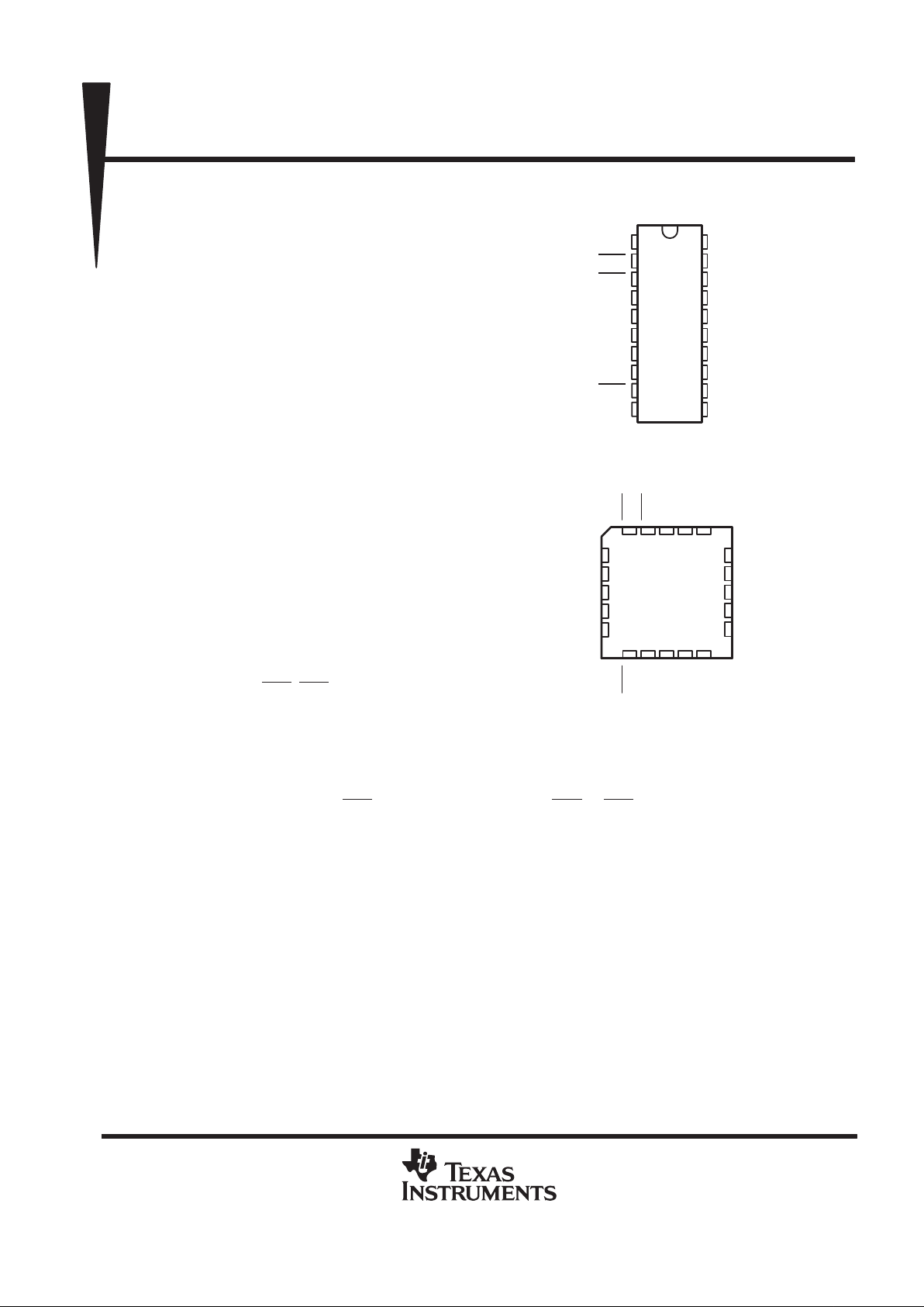
• Package Options Include Plastic
Small-Outline (DW) Packages, Ceramic
Chip Carriers (FK), and Standard Plastic (N)
and Ceramic (J) 300-mil DIPs
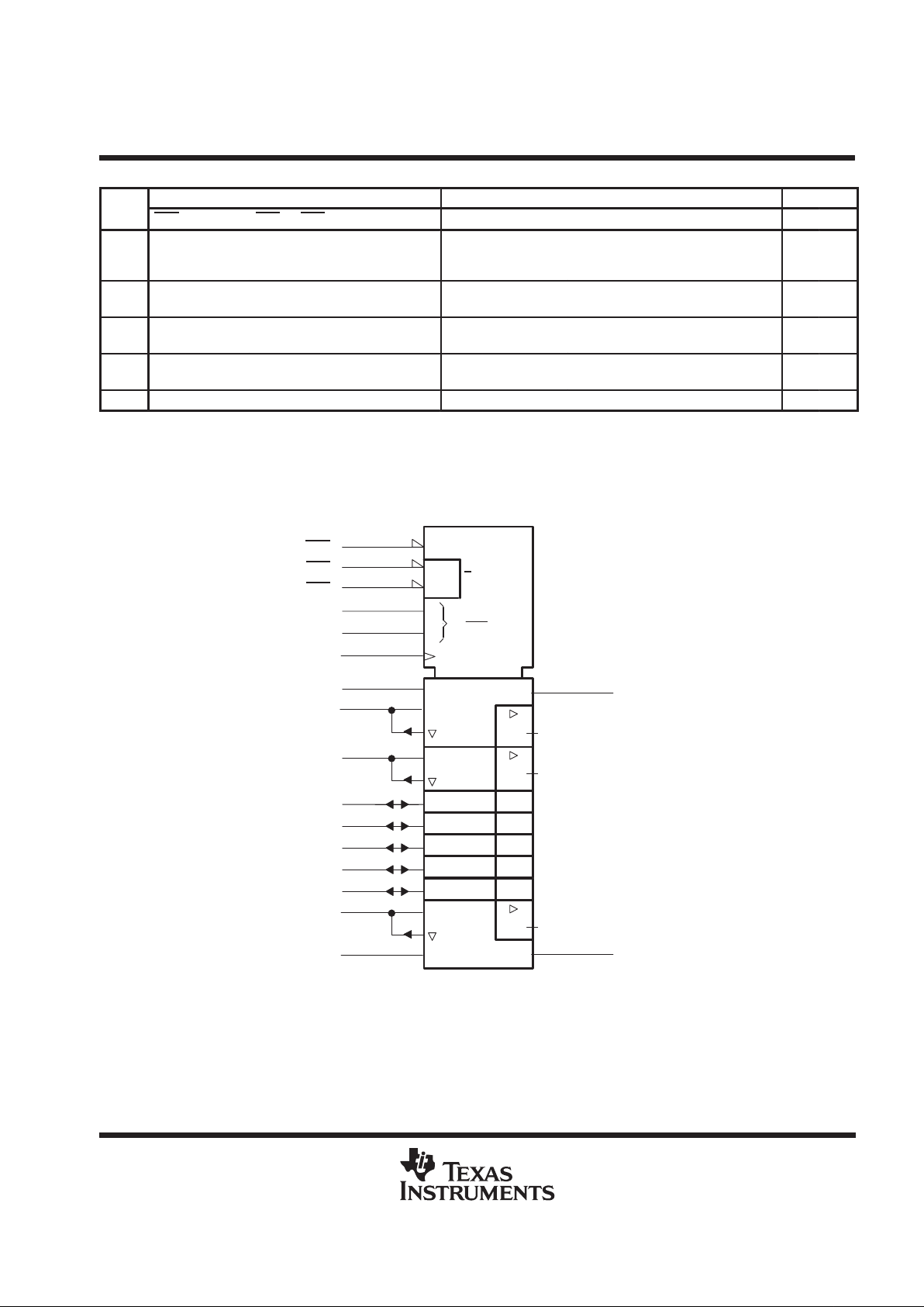
description
These 8-bit universal shift/storage registers
feature multiplexed input/output (I/O) ports to
achieve full 8-bit data handling in a 20-pin
package. Two function-select (S0, S1) inputs and
two output-enable (OE1
, OE2) inputs can be used
to choose the modes of operation listed in the
function table.
Synchronous parallel loading is accomplished by taking both S0 and S1 high. This places the 3-state outputs
in the high-impedance state and permits data applied on the I/O ports to be clocked into the register. Reading
out of the register can be accomplished while the outputs are enabled in any mode. Clearing occurs
synchronously when the clear (CLR
) input is low. Taking either OE1 or OE2 high disables the outputs but has
no effect on clearing, shifting, or storing data.
The SN54ALS323 is characterized for operation over the full military temperature range of –55°C to 125°C. The
SN74ALS323 is characterized for operation from 0°C to 70°C.
1
2
3
4
5
6
7
8
9
10
20
19
18
17
16
15
14
13
12
11
S0
OE1
OE2
G/Q
G
E/Q
E
C/Q
C
A/Q
A
Q
A′
CLR
GND
V
CC
S1
SL
Q
H′
H/Q
H
F/Q
F
D/Q
D
B/Q
B
CLK
SR
SN54ALS323 ...J PACKAGE
SN74ALS323 . . . DW OR N PACKAGE
(TOP VIEW)
3212019
910111213
4
5
6
7
8
18
17
16
15
14
SL
Q
H′
H/Q
H
F/Q
F
D/Q
D
G/Q
G
E/Q
E
C/Q
C
A/Q
A
Q
A′
OE2
OE1
S0
CLK
B/Q
S1
CLR
GND
SR
V
CC
SN54ALS323 . . . FK PACKAGE
(TOP VIEW)
B
PRODUCTION DATA information is current as of publication date.
Products conform to specifications per the terms of Texas Instruments
standard warranty. Production processing does not necessarily include
testing of all parameters.
SN54ALS323, SN74ALS323
8-BIT UNIVERSAL SHIFT/STORAGE REGISTERS
WITH SYNCHRONOUS CLEAR AND 3-STATE OUTPUTS
SDAS267A – DECEMBER 1982 – REVISED DECEMBER 1994
2
POST OFFICE BOX 655303 • DALLAS, TEXAS 75265
FUNCTION TABLE
INPUTS I/O PORTS OUTPUTS
MODE
CLR S1 S0 OE1†OE2†CLK SL SR A/QAB/QBC/QCD/QDE/QEF/QFG/QGH/QHQA′Q
H′
Clear
L
L
L
X
L
H
L
X
H
L
L
X
L
L
X
↑
↑
↑
X
X
X
X
X
X
L
L
X
L
L
X
L
L
X
L
L
X
L
L
X
L
L
X
L
L
X
L
L
X
L
L
L
L
L
L
Hold
HHLXL
XLL
L
L
XLXXXXQ
A0
Q
A0
Q
B0
Q
B0
Q
C0
Q
C0
Q
D0
Q
D0
Q
E0
Q
E0
Q
F0
Q
F0
Q
G0
Q
G0
Q
H0
Q
H0
Q
A0
Q
A0
Q
H0
Q
H0
Shift
RightHHLLHHLL
L
L
↑↑XXHLHLQ
An
Q
An
Q
Bn
Q
Bn
Q
Cn
Q
Cn
Q
Dn
Q
Dn
Q
En
Q
En
Q
Fn
Q
Fn
Q
Gn
Q
Gn
HLQ
Gn
Q
Gn
Shift
LeftHHHHLL
L
L
L
L
↑↑HLXXQ
Bn
Q
Bn
Q
Cn
Q
Cn
Q
Dn
Q
Dn
Q
En
Q
En
Q
Fn
Q
Fn
Q
Gn
Q
Gn
Q
Hn
Q
Hn
HLQ
Bn
Q
Bn
H
L
Load H H H X X ↑ X X a b c d e f g h a h
NOTE: a ...h = the level of the steady-state input at inputs A through H, respectively. This data is loaded into the flip-flops while the flip-flop outputs
are isolated from the I/O terminals.
†
When one or both output-enable inputs are high, the eight I/O terminals are disabled to the high-impedance state; however, sequ ential operation
or clearing of the register is not affected.
logic symbol
‡
SRG8
M
0
3
4R
9
6
14
5
15
4
8
2
3
0
1
S0
1
19
S1
12
CLK
5, 13
1,4D
11
SR
3,4D
7
6, 13
3, 4D
13
17
12, 13
2, 4D
18
SL
3, 4D
16
&
3
EN13
C4/1→/2←
Q
A′
Q
H′
CLR
OE1
OE2
A/Q
A
H/Q
H
B/Q
B
C/Q
C
D/Q
D
E/Q
E
F/Q
F
G/Q
G
Z5
Z6
Z12
‡
This symbol is in accordance with ANSI/IEEE Std 91-1984 and IEC Publication 617-12.
SN54ALS323, SN74ALS323
8-BIT UNIVERSAL SHIFT/STORAGE REGISTERS
WITH SYNCHRONOUS CLEAR AND 3-STATE OUTPUTS
SDAS267A – DECEMBER 1982 – REVISED DECEMBER 1994
3
POST OFFICE BOX 655303 • DALLAS, TEXAS 75265
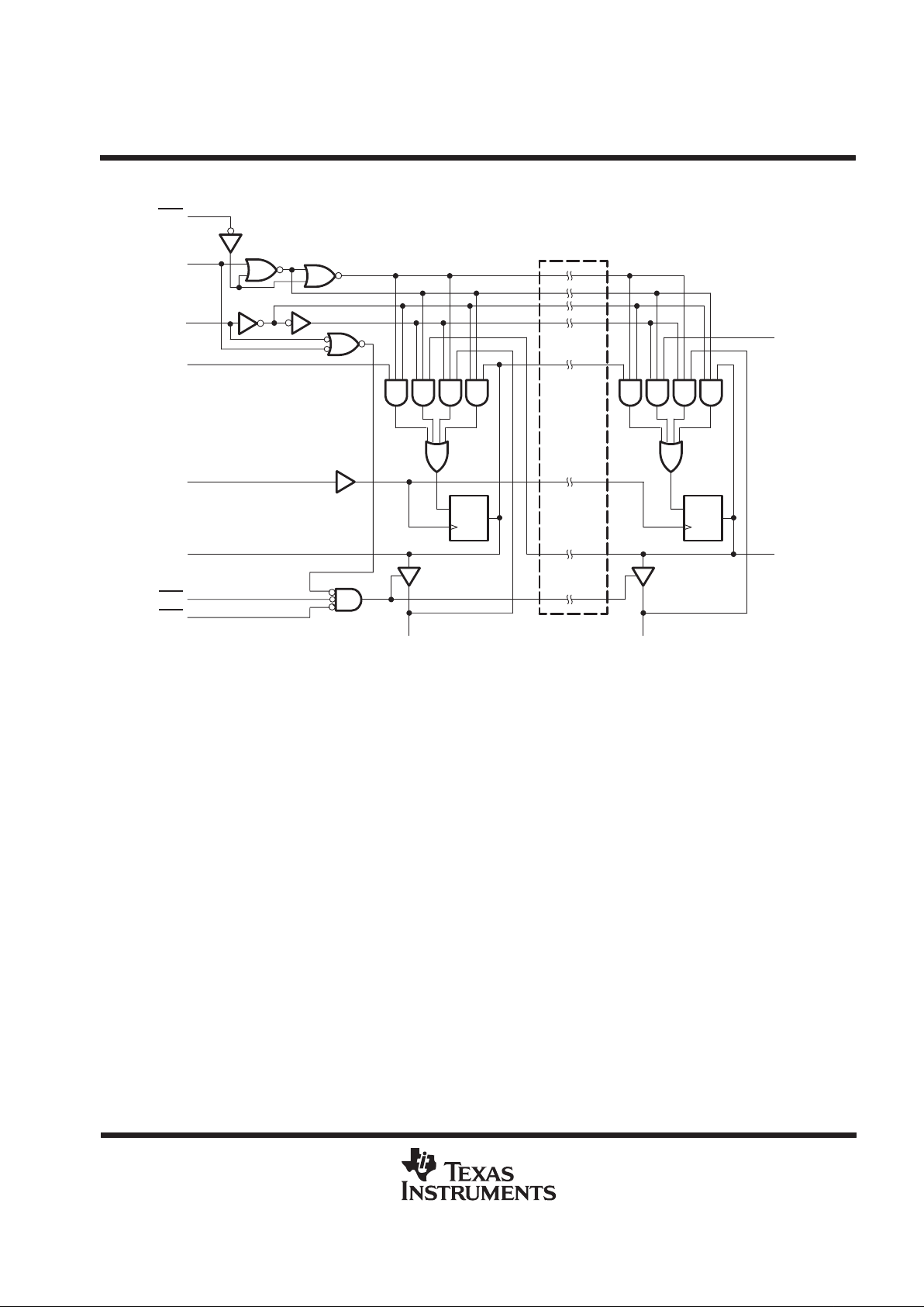
logic diagram (positive logic)
C1
1D
C1
1D
Six
Identical
Channels
Not
Shown
†
9
1
19
11
12
8
2
3
18
17
CLR
S0
S1
SR
(shift right
serial input)
CLK
Q
A′
OE1
OE2
SL
(shift left
serial input)
Q
H′
716
A/Q
A
H/Q
H
†
I/O ports not shown: B/QB (13), C/QC (6), D/QD (14), E/QE (5), F/QF (15), and G/QG (4).
absolute maximum ratings over operating free-air temperature range (unless otherwise noted)
‡
Supply voltage, V
CC
7 V. . . . . . . . . . . . . . . . . . . . . . . . . . . . . . . . . . . . . . . . . . . . . . . . . . . . . . . . . . . . . . . . . . . . . . . .
Input voltage, V
I
: All inputs 7 V. . . . . . . . . . . . . . . . . . . . . . . . . . . . . . . . . . . . . . . . . . . . . . . . . . . . . . . . . . . . . . . . . . .
I/O ports 5.5 V. . . . . . . . . . . . . . . . . . . . . . . . . . . . . . . . . . . . . . . . . . . . . . . . . . . . . . . . . . . . . . . . .
Operating free-air temperature range, T
A
: SN54ALS323 –55°C to 125°C. . . . . . . . . . . . . . . . . . . . . . . . . . . . .
SN74ALS323 0°C to 70°C. . . . . . . . . . . . . . . . . . . . . . . . . . . . . . . . .
Storage temperature range –65°C to 150°C. . . . . . . . . . . . . . . . . . . . . . . . . . . . . . . . . . . . . . . . . . . . . . . . . . . . . . .
‡
Stresses beyond those listed under “absolute maximum ratings” may cause permanent damage to the device. These are stress ratings only, and
functional operation of the device at these or any other conditions beyond those indicated under “recommended operating conditions” is not
implied. Exposure to absolute-maximum-rated conditions for extended periods may affect device reliability.

SN54ALS323, SN74ALS323
8-BIT UNIVERSAL SHIFT/STORAGE REGISTERS
WITH SYNCHRONOUS CLEAR AND 3-STATE OUTPUTS
SDAS267A – DECEMBER 1982 – REVISED DECEMBER 1994
4
POST OFFICE BOX 655303 • DALLAS, TEXAS 75265
recommended operating conditions
SN54ALS323 SN74ALS323
MIN NOM MAX MIN NOM MAX
UNIT
V
CC
Supply voltage 4.5 5 5.5 4.5 5 5.5 V
V
IH
High-level input voltage 2 2 V
V
IL
Low-level input voltage 0.7 0.8 V
p
QA′ or Q
H′
–0.4 –0.4
IOHHigh-level output current
QA thru Q
H
–1 –2.6
mA
p
QA′ or Q
H′
4 8
IOLLow-level output current
QA thru Q
H
12 24
mA
T
A
Operating free-air temperature –55 125 0 70 °C
electrical characteristics over recommended operating free-air temperature range (unless
otherwise noted)
SN54ALS323 SN74ALS323
PARAMETER
TEST CONDITIONS
MIN TYP†MAX MIN TYP†MAX
UNIT
V
IK
VCC = 4.5 V, II = –18 mA –1.5 –1.5 V
Any output VCC = 4.5 V to 5.5 V, IOH = – 0.4 mA VCC –2 VCC –2
V
OH
IOH = – 1 mA 2.4 3.3
V
Q
A
thru Q
H
V
CC
= 4.5
V
IOH = – 2.6 mA 2.4 3.2
IOL = 4 mA 0.25 0.4 0.25 0.4
Q
A′
or
Q
H′
V
CC
= 4.5
V
IOL = 8 mA 0.35 0.5
V
OL
IOL = 12 mA 0.25 0.4 0.25 0.4
V
Q
A
thru Q
H
V
CC
= 4.5
V
IOL = 24 mA 0.35 0.5
A thru H
VI = 5.5 V 0.1 0.1
I
I
Any others
V
CC
= 5.5
V
VI = 7 V 0.1 0.1
mA
I
IH
‡
VCC = 5.5 V, VI = 2.7 V 20 20 µA
S0, S1, SR, SL
–0.2 –0.2
I
IL
‡
Any others
V
CC
= 5.5 V,
V
I
= 0.4
V
–0.1 –0.1
mA
QA′ or Q
H′
–15 –70 –15 –70
I
OS
§
QA thru Q
H
V
CC
= 5.5 V,
V
O
= 2.25
V
–20 –112 –30 –112
mA
Outputs high 15 28 15 28
I
CC
VCC = 5.5 V
Outputs low 22 38 22 38
mA
Outputs disabled 23 40 23 40
†
All typical values are at VCC = 5 V, TA = 25°C.
‡
For I/O ports (QA thru QH), the parameters IIH and IIL include the off-state output current.
§
The output conditions have been chosen to produce a current that closely approximates one half of the true short-circuit output current, IOS.

SN54ALS323, SN74ALS323
8-BIT UNIVERSAL SHIFT/STORAGE REGISTERS
WITH SYNCHRONOUS CLEAR AND 3-STATE OUTPUTS
SDAS267A – DECEMBER 1982 – REVISED DECEMBER 1994
5
POST OFFICE BOX 655303 • DALLAS, TEXAS 75265
timing requirements over recommended ranges of supply voltage and operating free-air
temperature (unless otherwise noted)
SN54ALS323 SN74ALS323
MIN MAX MIN MAX
UNIT
f
clock
Clock frequency (at 50% duty cycle) 0 17 0 17 MHz
t
w
Pulse duration CLK high or low 22 16.5 ns
S0 or S1 25 20
High 18 16
t
su
Set
up time before
CLK↑
Serial
or parallel data
Low 15 6
ns
su
CLR active
25 20
Inactive-state setup time before CLK↑
†
CLR 18 16
S0 or S1 0 0
t
h
Hold ti
me after
CLK↑
Serial or parallel data
0 0
ns
†
Inactive-state setup time is also referred to as recovery time.
switching characteristics (see Figure 1)
PARAMETER
FROM
(INPUT)
TO
(OUTPUT)
VCC = 4.5 V to 5.5 V,
CL = 50 pF,
R1 = 500 Ω
,
R2 = 500 Ω,
TA = MIN to MAX
‡
UNIT
SN54ALS323 SN74ALS323
MIN MAX MIN MAX
f
max
17 17 MHz
t
PLH
2 19 4 13
t
PHL
CLK
Q
A
thru
Q
H
4 25 7 19
ns
t
PLH
2 21 5 15
t
PHL
CLK
Q
A′
or
Q
H′
4 25 8 18
ns
t
PZH
5 22 6 16
t
PZL
OE1, OE2
Q
A
thru
Q
H
6 27 8 22
ns
t
PZH
5 27 7 17
t
PZL
S0, S1
Q
A
thru
Q
H
6 27 8 22
ns
t
PHZ
1 15 1 8
t
PLZ
OE1, OE2
Q
A
thru
Q
H
4 38 5 15
ns
t
PHZ
1 16 1 12
t
PLZ
S0, S1
Q
A
thru Q
H
4 34 8 25
ns
‡
For conditions shown as MIN or MAX, use the appropriate value specified under recommended operating conditions.

SN54ALS323, SN74ALS323
8-BIT UNIVERSAL SHIFT/STORAGE REGISTERS
WITH SYNCHRONOUS CLEAR AND 3-STATE OUTPUTS
SDAS267A – DECEMBER 1982 – REVISED DECEMBER 1994
6
POST OFFICE BOX 655303 • DALLAS, TEXAS 75265
PARAMETER MEASUREMENT INFORMATION
SERIES 54ALS/74ALS AND 54AS/74AS DEVICES
t
PHZ
t
PLZ
t
PHL
t
PLH
0.3 V
t
PZL
t
PZH
t
PLH
t
PHL
LOAD CIRCUIT
FOR 3-STATE OUTPUTS
From Output
Under Test
Test
Point
R1
S1
C
L
(see Note A)
7 V
1.3 V
1.3 V1.3 V
3.5 V
3.5 V
0.3 V
0.3 V
t
h
t
su
VOLTAGE WAVEFORMS
SETUP AND HOLD TIMES
Timing
Input
Data
Input
1.3 V 1.3 V
3.5 V
3.5 V
0.3 V
0.3 V
High-Level
Pulse
Low-Level
Pulse
t
w
VOLTAGE WAVEFORMS
PULSE DURATIONS
Input
Out-of-Phase
Output
(see Note C)
1.3 V 1.3 V
1.3 V1.3 V
1.3 V 1.3 V
1.3 V1.3 V
1.3 V
1.3 V
3.5 V
3.5 V
0.3 V
0.3 V
V
OL
V
OH
V
OH
V
OL
Output
Control
(low-level
enabling)
Waveform 1
S1 Closed
(see Note B)
Waveform 2
S1 Open
(see Note B)
[
0 V
V
OH
V
OL
[
3.5 V
In-Phase
Output
0.3 V
1.3 V 1.3 V
VOLTAGE WAVEFORMS
PROPAGATION DELAY TIMES
VOLTAGE WAVEFORMS
ENABLE AND DISABLE TIMES, 3-STATE OUTPUTS
R2
V
CC
R
L
Test
Point
From Output
Under Test
C
L
(see Note A)
LOAD CIRCUIT
FOR OPEN-COLLECTOR OUTPUTS
LOAD CIRCUIT FOR
BI-STATE
TOTEM-POLE OUTPUTS
From Output
Under Test
Test
Point
C
L
(see Note A)
R
L
RL = R1 = R2
NOTES: A. CL includes probe and jig capacitance.
B. Waveform 1 is for an output with internal conditions such that the output is low except when disabled by the output control.
Waveform 2 is for an output with internal conditions such that the output is high except when disabled by the output control.
C. When measuring propagation delay items of 3-state outputs, switch S1 is open.
D. All input pulses have the following characteristics: PRR ≤ 1 MHz, tr = tf = 2 ns, duty cycle = 50%.
E. The outputs are measured one at a time with one transition per measurement.
Figure 1. Load Circuits and Voltage Waveforms

IMPORTANT NOTICE
T exas Instruments and its subsidiaries (TI) reserve the right to make changes to their products or to discontinue
any product or service without notice, and advise customers to obtain the latest version of relevant information
to verify, before placing orders, that information being relied on is current and complete. All products are sold
subject to the terms and conditions of sale supplied at the time of order acknowledgement, including those
pertaining to warranty, patent infringement, and limitation of liability.
TI warrants performance of its semiconductor products to the specifications applicable at the time of sale in
accordance with TI’s standard warranty. Testing and other quality control techniques are utilized to the extent
TI deems necessary to support this warranty. Specific testing of all parameters of each device is not necessarily
performed, except those mandated by government requirements.
CERT AIN APPLICATIONS USING SEMICONDUCTOR PRODUCTS MA Y INVOLVE POTENTIAL RISKS OF
DEATH, PERSONAL INJURY, OR SEVERE PROPERTY OR ENVIRONMENTAL DAMAGE (“CRITICAL
APPLICATIONS”). TI SEMICONDUCTOR PRODUCTS ARE NOT DESIGNED, AUTHORIZED, OR
WARRANTED TO BE SUITABLE FOR USE IN LIFE-SUPPORT DEVICES OR SYSTEMS OR OTHER
CRITICAL APPLICATIONS. INCLUSION OF TI PRODUCTS IN SUCH APPLICA TIONS IS UNDERST OOD TO
BE FULLY AT THE CUSTOMER’S RISK.
In order to minimize risks associated with the customer’s applications, adequate design and operating
safeguards must be provided by the customer to minimize inherent or procedural hazards.
TI assumes no liability for applications assistance or customer product design. TI does not warrant or represent
that any license, either express or implied, is granted under any patent right, copyright, mask work right, or other
intellectual property right of TI covering or relating to any combination, machine, or process in which such
semiconductor products or services might be or are used. TI’s publication of information regarding any third
party’s products or services does not constitute TI’s approval, warranty or endorsement thereof.
Copyright 1998, Texas Instruments Incorporated
 Loading...