

Datasheet SN54ALS193AJ, SN74ALS193AD, SN74ALS193ADR, SN74ALS193AN, SNJ54ALS193AFK Datasheet (Texas Instruments)
...
SN54ALS193A, SN74ALS193A
SYNCHRONOUS 4-BIT UP/DOWN BINARY COUNTERS
WITH DUAL CLOCK AND CLEAR
SDAS211C – DECEMBER 1982 – REVISED JULY 1996
1
POST OFFICE BOX 655303 • DALLAS, TEXAS 75265
D
Look-Ahead Circuitry Enhances Cascaded
Counters
D
Fully Synchronous in Count Modes
D
Parallel Asynchronous Load for Modulo-N
Count Lengths
D
Asynchronous Clear
D
Package Options Include Plastic
Small-Outline (D) Packages, Ceramic Chip
Carriers (FK), and Standard Plastic (N) and
Ceramic (J) 300-mil DIPs
description
The ’ALS193A are synchronous, reversible, 4-bit
up/down binary counters. Synchronous counting
operation is provided by having all flip-flops
clocked simultaneously so that the outputs
change coincident with each other when
instructed by the steering logic. This mode of
operation eliminates the output counting spikes
normally associated with asynchronous (rippleclock) counters.
The outputs of the four flip-flops are triggered on
a low-to-high-level transition of either count/clock
(UP or DOWN) input. The direction of the count is
determined by which count input is pulsed while
the other count input is high.
All four counters are fully programmable; that is, each output may be preset to either level by placing a low on
the load (LOAD
) input and entering the desired data at the data inputs. The output changes to agree with the
data inputs independently of the count pulses. This feature allows the counters to be used as modulo-N dividers
by simply modifying the count length with the preset inputs.
A high level applied to the clear (CLR) input forces all outputs to the low level. The clear function is independent
of the count and LOAD
inputs. The UP, DOWN, and LOAD inputs are buffered to lower the drive requirement,
which significantly reduces the loading on, or current required by, clock drivers, etc., for long parallel words.
These counters are designed to be cascaded without the need for external circuitry. The borrow (BO
) output
produces a low-level pulse while the count is zero (all Q outputs low) and the DOWN input is low. Similarily, the
carry (CO
) output produces a low-level pulse while the count is 9 or 15 (all Q outputs high) and the UP input
is low. The counters can then be easily cascaded by feeding BO
and CO to the count-down and count-up inputs,
respectively, of the succeeding counter.
The SN54ALS193A is characterized for operation over the full military temperature range of –55°C to 125°C.
The SN74ALS193A is characterized for operation from 0°C to 70°C.
Copyright 1996, Texas Instruments Incorporated
PRODUCTION DATA information is current as of publication date.
Products conform to specifications per the terms of Texas Instruments
standard warranty. Production processing does not necessarily include
testing of all parameters.
Please be aware that an important notice concerning availability, standard warranty, and use in critical applications of
Texas Instruments semiconductor products and disclaimers thereto appears at the end of this data sheet.
1
2
3
4
5
6
7
8
16
15
14
13
12
11
10
9
B
Q
B
Q
A
DOWN
UP
Q
C
Q
D
GND
V
CC
A
CLR
BO
CO
LOAD
C
D
SN54ALS193A ...J PACKAGE
SN74ALS193A ...D OR N PACKAGE
(TOP VIEW)
SN54ALS193A . . . FK PACKAGE
(TOP VIEW)
3212019
910111213
4
5
6
7
8
18
17
16
15
14
CLR
BO
NC
CO
LOAD
Q
A
DOWN
NC
UP
Q
C
B
NC
D
C
A
Q
GND
NC
D
Q
B
V
CC
NC – No internal connection
SN54ALS193A, SN74ALS193A
SYNCHRONOUS 4-BIT UP/DOWN BINARY COUNTERS
WITH DUAL CLOCK AND CLEAR
SDAS211C – DECEMBER 1982 – REVISED JULY 1996
2
POST OFFICE BOX 655303 • DALLAS, TEXAS 75265
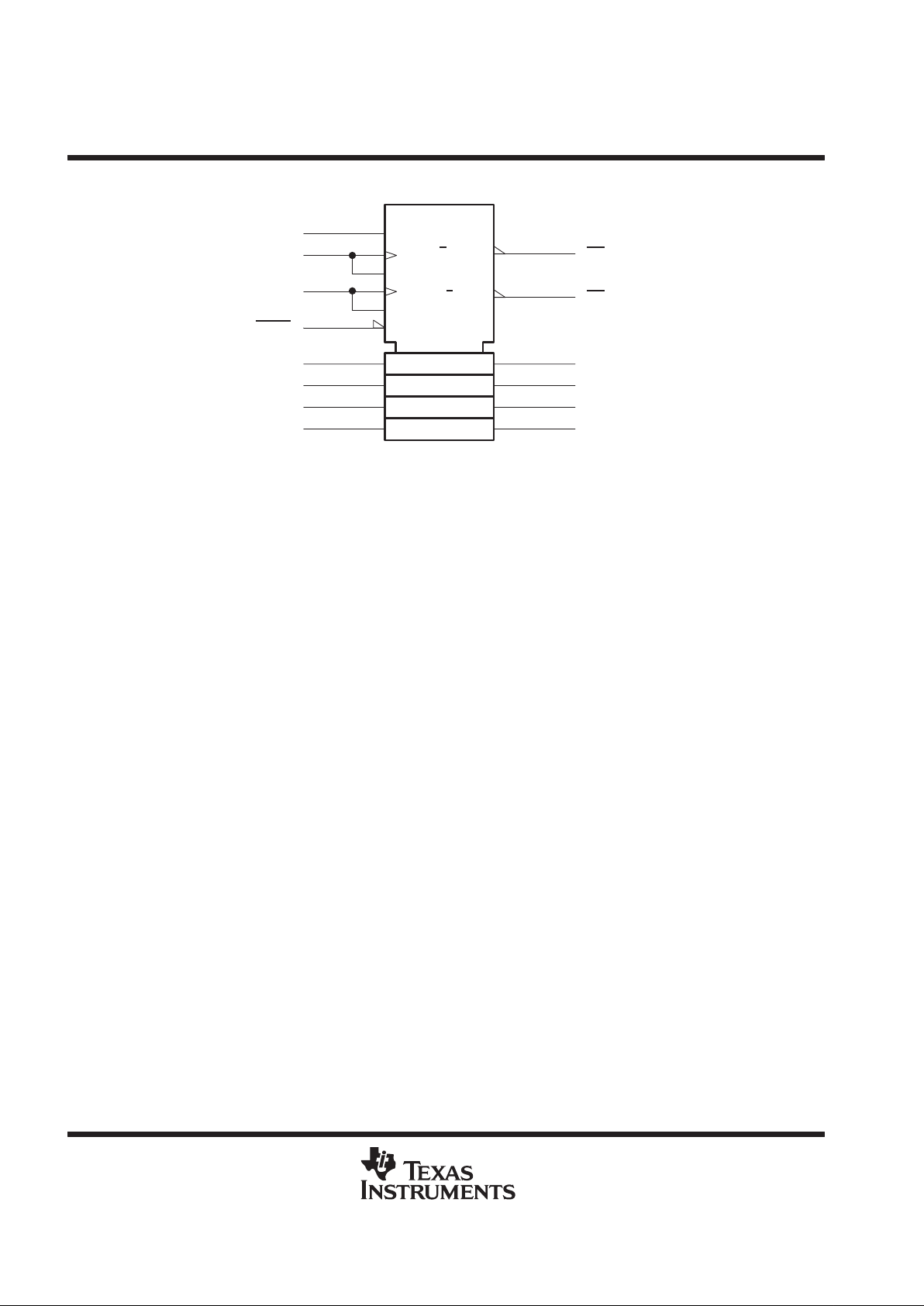
logic symbol
†
CTRDIV16
LOAD
CO1CT = 15
2CT = 0
12
3D
15
A
1
B
10
C
9
D
CT = 0
14
CLR
2+
G1
C3
11
5
UP
1–
G2
4
DOWN
13
3
2
6
7
BO
Q
A
Q
B
Q
C
Q
D
[1]
[2]
[4]
[8]
†
This symbol is in accordance with ANSI/IEEE Std 91-1984 and IEC Publication 617-12.
Pin numbers shown are for the D, J, and N packages.

SN54ALS193A, SN74ALS193A
SYNCHRONOUS 4-BIT UP/DOWN BINARY COUNTERS
WITH DUAL CLOCK AND CLEAR
SDAS211C – DECEMBER 1982 – REVISED JULY 1996
3
POST OFFICE BOX 655303 • DALLAS, TEXAS 75265
logic diagram (positive logic)
15
4
5
CO
A
1
10
9
B
C
D
UP
DOWN
Q
A
Q
B
Q
C
Q
D
12
13
3
2
6
7
1D
R
CLR
LOAD
S
R
S
R
R
R
1D
1D
1D
C1
C1
C1
C1
S
S
S
BO
14
11
Pin numbers shown are for the D, J, and N packages.

SN54ALS193A, SN74ALS193A
SYNCHRONOUS 4-BIT UP/DOWN BINARY COUNTERS
WITH DUAL CLOCK AND CLEAR
SDAS211C – DECEMBER 1982 – REVISED JULY 1996
4
POST OFFICE BOX 655303 • DALLAS, TEXAS 75265
typical clear, load, and count sequence
the following sequence is illustrated below:
1. Clear outputs to zero
2. Load (preset) to binary 13
3. Count up to 14, 15 (carry), 0, 1, and 2
4. Count down to 1, 0 (borrow), 15, 14, and 13
0
A
B
C
D
UP
DOWN
Q
A
Q
D
Q
C
Q
B
Count Up Count Down
13 0 2110
Data
Inputs
CLR
Data
Outputs
LOAD
CO
BO
14 15 15 14 13
Sequence
Illustrated
Clear Preset
NOTES: A. Clear overrides load, data, and count inputs.
B. When counting up, count-down input must be high; when counting down, count-up input must be high.

SN54ALS193A, SN74ALS193A
SYNCHRONOUS 4-BIT UP/DOWN BINARY COUNTERS
WITH DUAL CLOCK AND CLEAR
SDAS211C – DECEMBER 1982 – REVISED JULY 1996
5
POST OFFICE BOX 655303 • DALLAS, TEXAS 75265
absolute maximum ratings over operating free-air temperature range (unless otherwise noted)
†
Supply voltage, V
CC
7 V. . . . . . . . . . . . . . . . . . . . . . . . . . . . . . . . . . . . . . . . . . . . . . . . . . . . . . . . . . . . . . . . . . . . . . .
Input voltage, V
I
7 V. . . . . . . . . . . . . . . . . . . . . . . . . . . . . . . . . . . . . . . . . . . . . . . . . . . . . . . . . . . . . . . . . . . . . . . . . . .
Operating free-air temperature range, T
A
: SN54ALS193A –55°C to 125°C. . . . . . . . . . . . . . . . . . . . . . . . . . . .
SN74ALS193A 0°C to 70°C. . . . . . . . . . . . . . . . . . . . . . . . . . . . . . .
Storage temperature range, T
stg
–65°C to 150°C. . . . . . . . . . . . . . . . . . . . . . . . . . . . . . . . . . . . . . . . . . . . . . . . . .
†
Stresses beyond those listed under “absolute maximum ratings” may cause permanent damage to the device. These are stress ratings only, and
functional operation of the device at these or any other conditions beyond those indicated under “recommended operating conditions” is not
implied. Exposure to absolute-maximum-rated conditions for extended periods may affect device reliability.
recommended operating conditions
SN54ALS193A SN74ALS193A
MIN NOM MAX MIN NOM MAX
UNIT
V
CC
Supply voltage 4.5 5 5.5 4.5 5 5.5 V
V
IH
High-level input voltage 2 2 V
V
IL
Low-level input voltage 0.7 0.8 V
I
OH
High-level output current –0.4 –0.4 mA
I
OL
Low-level output current 4 8 mA
f
clock
Clock frequency 0 20 0 30 MHz
CLR high 10 10
t
w
Pulse duration
LOAD
low 25 20
ns
UP or DOWN high or low 30 16.5
Data before LOAD↑ 25 20
t
su
Setup time
CLR inactive before UP or DOWN
20 20
ns
LOAD inactive before UP or DOWN 20 20
Data after LOAD↑ 5 5
t
h
Hold time
UP high after DOWN↑
5 0
ns
DOWN high after UP↑ 5 0
T
A
Operating free-air temperature –55 125 0 70 °C
electrical characteristics over recommended operating free-air temperature range (unless
otherwise noted)
SN54ALS193A SN74ALS193A
PARAMETER
TEST CONDITIONS
MIN TYP‡MAX MIN TYP‡MAX
UNIT
V
IK
VCC = 4.5 V, II = –18 mA –1.5 –1.5 V
V
OH
VCC = 4.5 V to 5.5 V, IOH = –0.4 mA VCC–2 VCC–2 V
IOL = 4 mA 0.25 0.4 0.25 0.4
VOLV
CC
= 4.5
V
IOL = 8 mA 0.35 0.5
V
I
I
VCC = 5.5 V, VI = 7 V 0.1 0.35 0.1 mA
I
IH
VCC = 5.5 V, VI = 2.7 V 20 20 µA
UP or DOWN
–0.2 –0.2
I
IL
All others
V
CC
= 5.5 V,
V
I
= 0.4
V
–0.1 –0.1
mA
I
O
§
VCC = 5.5 V, VO = 2.25 V –20 –112 –30 –112 mA
I
CC
VCC = 5.5 V, See Note 1 12 22 12 22 mA
‡
All typical values are at VCC = 5 V, TA = 25°C.
§
The output conditions have been chosen to produce a current that closely approximates one half of the true short-circuit output current, IOS.
NOTE 1: ICC is measured with the clear and load inputs grounded and all other inputs at 4.5 V .

SN54ALS193A, SN74ALS193A
SYNCHRONOUS 4-BIT UP/DOWN BINARY COUNTERS
WITH DUAL CLOCK AND CLEAR
SDAS211C – DECEMBER 1982 – REVISED JULY 1996
6
POST OFFICE BOX 655303 • DALLAS, TEXAS 75265
switching characteristics (see Figure 1)
PARAMETER
FROM
(
INPUT
)
TO
(
OUTPUT
)
VCC = 4.5 V to 5.5 V,
CL = 50 pF,
R1 = R2 = 500 Ω
,
TA = MIN to MAX
†
UNIT
(INPUT)
(OUTPUT)
SN54ALS193A SN74ALS193A
MIN MAX MIN MAX
f
max
25 30 MHz
t
PLH
3 20 3 16
t
PHL
UP
CO
3 21 5 18
ns
t
PLH
4 20 4 16
t
PHL
DOWN
BO
5 22 5 18
ns
t
PLH
3 27 3 19
t
PHL
UP or DOWN
Any Q
4 23 4 17
ns
t
PLH
7 38 7 30
t
PHL
LOAD
Any Q
8 37 8 28
ns
t
PHL
CLR Any Q 5 20 5 17 ns
†
For conditions shown MIN or MAX, use the appropriate value specified under recommended operating conditions.

SN54ALS193A, SN74ALS193A
SYNCHRONOUS 4-BIT UP/DOWN BINARY COUNTERS
WITH DUAL CLOCK AND CLEAR
SDAS211C – DECEMBER 1982 – REVISED JULY 1996
7
POST OFFICE BOX 655303 • DALLAS, TEXAS 75265
PARAMETER MEASUREMENT INFORMATION
SERIES 54ALS/74ALS AND 54AS/74AS DEVICES
t
PHZ
t
PLZ
t
PHL
t
PLH
0.3 V
t
PZL
t
PZH
t
PLH
t
PHL
LOAD CIRCUIT
FOR 3-STATE OUTPUTS
From Output
Under Test
Test
Point
R1
S1
C
L
(see Note A)
7 V
1.3 V
1.3 V1.3 V
3.5 V
3.5 V
0.3 V
0.3 V
t
h
t
su
VOLTAGE WAVEFORMS
SETUP AND HOLD TIMES
Timing
Input
Data
Input
1.3 V 1.3 V
3.5 V
3.5 V
0.3 V
0.3 V
High-Level
Pulse
Low-Level
Pulse
t
w
VOLTAGE WAVEFORMS
PULSE DURATIONS
Input
Out-of-Phase
Output
(see Note C)
1.3 V 1.3 V
1.3 V1.3 V
1.3 V 1.3 V
1.3 V1.3 V
1.3 V
1.3 V
3.5 V
3.5 V
0.3 V
0.3 V
V
OL
V
OH
V
OH
V
OL
Output
Control
(low-level
enabling)
Waveform 1
S1 Closed
(see Note B)
Waveform 2
S1 Open
(see Note B)
[
0 V
V
OH
V
OL
[
3.5 V
In-Phase
Output
0.3 V
1.3 V 1.3 V
VOLTAGE WAVEFORMS
PROPAGATION DELAY TIMES
VOLTAGE WAVEFORMS
ENABLE AND DISABLE TIMES, 3-STATE OUTPUTS
R2
V
CC
R
L
Test
Point
From Output
Under Test
C
L
(see Note A)
LOAD CIRCUIT
FOR OPEN-COLLECTOR OUTPUTS
LOAD CIRCUIT FOR
BI-STATE
TOTEM-POLE OUTPUTS
From Output
Under Test
Test
Point
C
L
(see Note A)
R
L
RL = R1 = R2
NOTES: A. CL includes probe and jig capacitance.
B. Waveform 1 is for an output with internal conditions such that the output is low except when disabled by the output control.
Waveform 2 is for an output with internal conditions such that the output is high except when disabled by the output control.
C. When measuring propagation delay items of 3-state outputs, switch S1 is open.
D. All input pulses have the following characteristics: PRR ≤ 1 MHz, tr = tf = 2 ns, duty cycle = 50%.
E. The outputs are measured one at a time with one transition per measurement.
Figure 1. Load Circuits and Voltage Waveforms

IMPORTANT NOTICE
T exas Instruments and its subsidiaries (TI) reserve the right to make changes to their products or to discontinue
any product or service without notice, and advise customers to obtain the latest version of relevant information
to verify, before placing orders, that information being relied on is current and complete. All products are sold
subject to the terms and conditions of sale supplied at the time of order acknowledgement, including those
pertaining to warranty, patent infringement, and limitation of liability.
TI warrants performance of its semiconductor products to the specifications applicable at the time of sale in
accordance with TI’s standard warranty. Testing and other quality control techniques are utilized to the extent
TI deems necessary to support this warranty. Specific testing of all parameters of each device is not necessarily
performed, except those mandated by government requirements.
CERT AIN APPLICATIONS USING SEMICONDUCTOR PRODUCTS MAY INVOLVE POTENTIAL RISKS OF
DEATH, PERSONAL INJURY, OR SEVERE PROPERTY OR ENVIRONMENTAL DAMAGE (“CRITICAL
APPLICATIONS”). TI SEMICONDUCTOR PRODUCTS ARE NOT DESIGNED, AUTHORIZED, OR
WARRANTED TO BE SUITABLE FOR USE IN LIFE-SUPPORT DEVICES OR SYSTEMS OR OTHER
CRITICAL APPLICATIONS. INCLUSION OF TI PRODUCTS IN SUCH APPLICA TIONS IS UNDERST OOD TO
BE FULLY AT THE CUSTOMER’S RISK.
In order to minimize risks associated with the customer’s applications, adequate design and operating
safeguards must be provided by the customer to minimize inherent or procedural hazards.
TI assumes no liability for applications assistance or customer product design. TI does not warrant or represent
that any license, either express or implied, is granted under any patent right, copyright, mask work right, or other
intellectual property right of TI covering or relating to any combination, machine, or process in which such
semiconductor products or services might be or are used. TI’s publication of information regarding any third
party’s products or services does not constitute TI’s approval, warranty or endorsement thereof.
Copyright 1998, Texas Instruments Incorporated
 Loading...