

Page 1
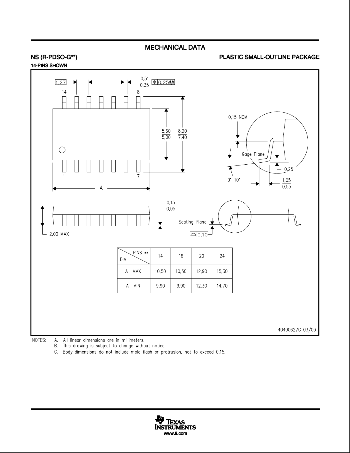
SOIC
D
AHC139
TSSOP
PW
HA139
查询SN54AHC139供应商
D
Operating Range 2-V to 5.5-V V
D
Designed Specifically for High-Speed
Memory Decoders and Data-Transmission
Systems
D
Incorporate Two Enable Inputs to Simplify
Cascading and/or Data Reception
SN54AHC139 ...J OR W PACKAGE
SN74AHC139 . . . D, DB, DGV, N, NS
OR PW PACKAGE
(TOP VIEW)
1G
1
2
1A
3
1B
4
1Y0
5
1Y1
6
1Y2
7
1Y3
GND
8
16
15
14
13
12
11
10
V
2G
2A
2B
2Y0
2Y1
2Y2
9
2Y3
CC
SN54AHC139, SN74AHC139
DUAL 2-LINE TO 4-LINE DECODERS/DEMULTIPLEXERS
SCLS259K – DECEMBER 1995 – REVISED MARCH 2003
D
CC
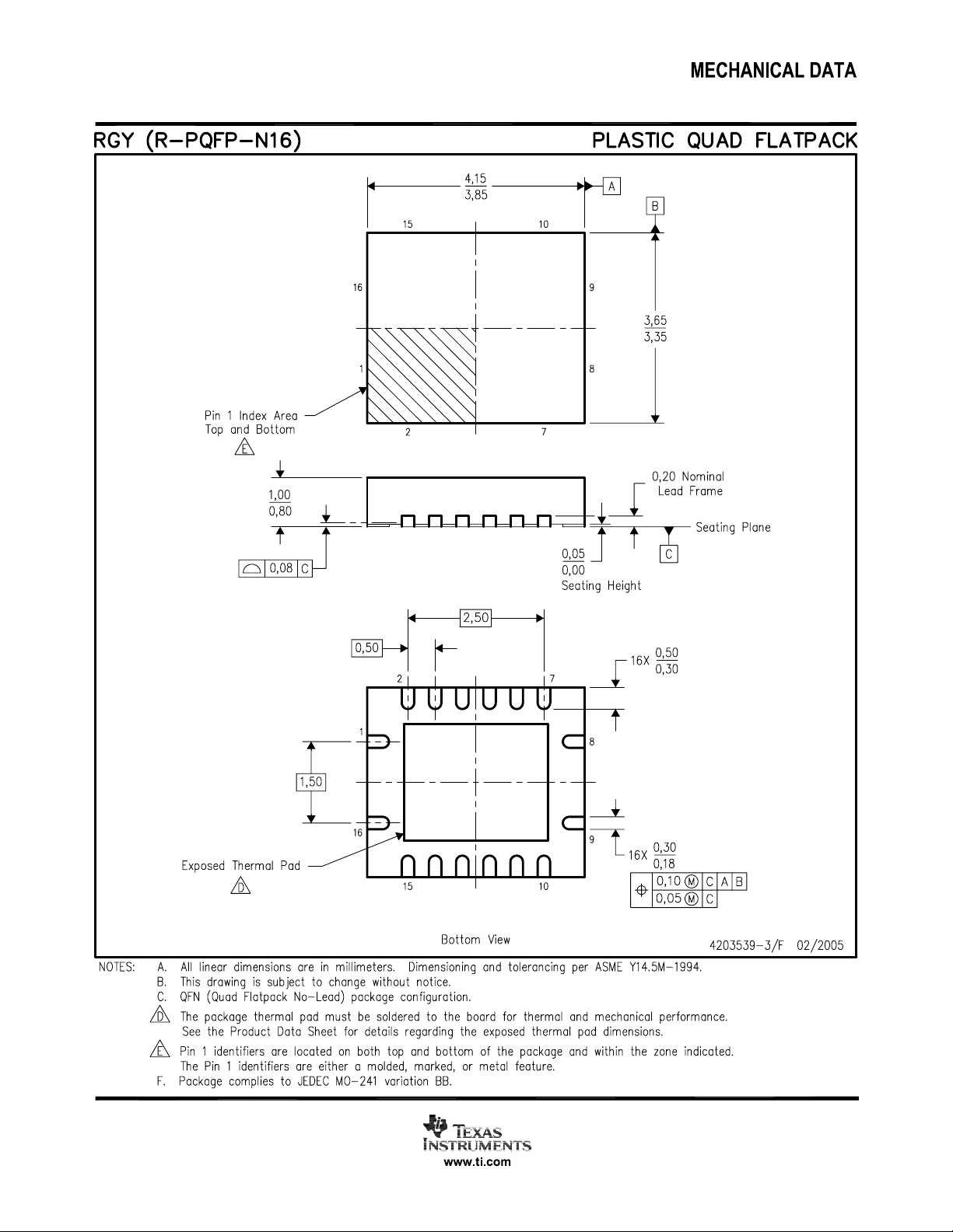
SN74AHC139 . . . RGY PACKAGE
(TOP VIEW)
1G
116
2
1A
3
1B
4
1Y0
5
1Y1
6
1Y2
7
1Y3
89
GND
Latch-Up Performance Exceeds 250 mA Per
JESD 17
D
ESD Protection Exceeds JESD 22
– 2000-V Human-Body Model (A114-A)
– 200-V Machine Model (A115-A)
– 1000-V Charged-Device Model (C101)
CC
V
2Y3
15
14
13
12
11
10
2G
2A
2B
2Y0
2Y1
2Y2
SN54AHC139 ...FK PACKAGE
1B
1Y0
NC
1Y1
1Y2
NC – No internal connection
(TOP VIEW)
1A1GNC
3212019
4
5
6
7
8
910111213
NC
1Y3
GND
CC
V
2Y3
2G
18
17
16
15
14
2Y2
2A
2B
NC
2Y0
2Y1
description/ordering information
The ’AHC139 devices are dual 2-line to 4-line decoders/demultiplexers designed for 2-V to 5.5-V VCC operation.
These devices are designed to be used in high-performance memory-decoding or data-routing applications
requiring very short propagation delay times. In high-performance memory systems, these decoders can be
used to minimize the effects of system decoding. When used with high-speed memories utilizing a fast enable
circuit, the delay times of these decoders and the enable time of the memory usually are less than the typical
access time of the memory . This means that the effective system delay introduced by the decoders is negligible.
ORDERING INFORMATION
T
A
QFN – RGY Tape and reel SN74AHC139RGYR HA139
PDIP – N Tube SN74AHC139N SN74AHC139N
–40°C to 85°C
–55°C to 125°C
†
Package drawings, standard packing quantities, thermal data, symbolization, and PCB design guidelines
are available at www.ti.com/sc/package.
SOP – NS Tape and reel SN74AHC139NSR AHC139
SSOP – DB Tape and reel SN74AHC139DBR HA139
TVSOP – DGV Tape and reel SN74AHC139DGVR HA139
CDIP – J Tube SNJ54AHC139J SNJ54AHC139J
CFP – W Tube SNJ54AHC139W SNJ54AHC139W
LCCC – FK Tube SNJ54AHC139FK SNJ54AHC139FK
PACKAGE
–
–
†
Tube SN74AHC139D
Tape and reel SN74AHC139DR
Tube SN74AHC139PW
Tape and reel SN74AHC139PWR
ORDERABLE
PART NUMBER
TOP-SIDE
MARKING
Please be aware that an important notice concerning availability, standard warranty, and use in critical applications of
Texas Instruments semiconductor products and disclaimers thereto appears at the end of this data sheet.
UNLESS OTHERWISE NOTED this document contains PRODUCTION
DATA information current as of publication date. Products conform to
specifications per the terms of Texas Instruments standard warranty.
Production processing does not necessarily include testing of all
parameters.
POST OFFICE BOX 655303 • DALLAS, TEXAS 75265
Copyright 2003, Texas Instruments Incorporated
1
Page 2
SN54AHC139, SN74AHC139
OUTPUTS
G
DUAL 2-LINE TO 4-LINE DECODERS/DEMULTIPLEXERS
SCLS259K – DECEMBER 1995 – REVISED MARCH 2003
description/ordering information (continued)
The active-low enable (G) input can be used as a data line in demultiplexing applications. These
decoders/demultiplexers feature fully buffered inputs, each of which represents only one normalized load to its
driving circuit.
FUNCTION TABLE
(each decoder/demultiplexer)
INPUTS
SELECT
B A Y0 Y1 Y2 Y3
H X X H H H H
L L LLHHH
L L HHLHH
L H LHHLH
L H H H H H L
logic diagram (positive logic)
1
1G
2
Select
Inputs
Select
Inputs
Pin numbers shown are for the D, DB, DGV , J, N, NS, PW , RGY, and W packages.
1A
1B
2G
2A
2B
3
15
14
13
12
11
10
4
1Y0
5
1Y1
6
1Y2
7
1Y3
Data
Outputs
2Y0
2Y1
2Y2
9
2Y3
2
POST OFFICE BOX 655303 • DALLAS, TEXAS 75265
Page 3
UNIT
mA
mA
∆t/∆v
Input transition rise or fall rate
ns/V
SN54AHC139, SN74AHC139
DUAL 2-LINE TO 4-LINE DECODERS/DEMULTIPLEXERS
SCLS259K – DECEMBER 1995 – REVISED MARCH 2003
absolute maximum ratings over operating free-air temperature range (unless otherwise noted)
Supply voltage range, V
Input voltage range, V
Output voltage range, V
Input clamp current, I
Output clamp current, I
Continuous output current, I
Continuous current through V
Package thermal impedance, θ
–0.5 V to 7 V. . . . . . . . . . . . . . . . . . . . . . . . . . . . . . . . . . . . . . . . . . . . . . . . . . . . . . . . . .
CC
(see Note 1) –0.5 V to 7 V. . . . . . . . . . . . . . . . . . . . . . . . . . . . . . . . . . . . . . . . . . . . . . . . . .
I
(see Note 1) –0.5 V to V
O
(V
< 0) –20 mA. . . . . . . . . . . . . . . . . . . . . . . . . . . . . . . . . . . . . . . . . . . . . . . . . . . . . . . . . . .
IK
I
(V
OK
< 0 or VO > VCC) ±20 mA. . . . . . . . . . . . . . . . . . . . . . . . . . . . . . . . . . . . . . . . . . . .
O
(V
= 0 to VCC) ±25 mA. . . . . . . . . . . . . . . . . . . . . . . . . . . . . . . . . . . . . . . . . . . . . .
O
O
or GND ±75 mA. . . . . . . . . . . . . . . . . . . . . . . . . . . . . . . . . . . . . . . . . . . . . . . . . . .
CC
(see Note 2): D package 73°C/W. . . . . . . . . . . . . . . . . . . . . . . . . . . . . . . . . . .
JA
CC
†
+ 0.5 V. . . . . . . . . . . . . . . . . . . . . . . . . . . . . . . . . . . . . . . .
(see Note 2): DB package 82°C/W. . . . . . . . . . . . . . . . . . . . . . . . . . . . . . . . .
(see Note 2): DGV package 120°C/W. . . . . . . . . . . . . . . . . . . . . . . . . . . . . . .
(see Note 2): N package 67°C/W. . . . . . . . . . . . . . . . . . . . . . . . . . . . . . . . . . .
(see Note 2): NS package 64°C/W. . . . . . . . . . . . . . . . . . . . . . . . . . . . . . . . .
(see Note 2): PW package 108°C/W. . . . . . . . . . . . . . . . . . . . . . . . . . . . . . . .
(see Note 3): RGY package 39°C/W. . . . . . . . . . . . . . . . . . . . . . . . . . . . . . . .
Storage temperature range, T
†
Stresses beyond those listed under “absolute maximum ratings” may cause permanent damage to the device. These are stress ratings only, and
functional operation of the device at these or any other conditions beyond those indicated under “recommended operating conditions” is not
implied. Exposure to absolute-maximum-rated conditions for extended periods may affect device reliability.
NOTES: 1. The input and output voltage ratings may be exceeded if the input and output current ratings are observed.
2. The package thermal impedance is calculated in accordance with JESD 51-7.
3. The package thermal impedance is calculated in accordance with JESD 51-5.
–65°C to 150°C. . . . . . . . . . . . . . . . . . . . . . . . . . . . . . . . . . . . . . . . . . . . . . . . . . .
stg
recommended operating conditions (see Note 4)
SN54AHC139 SN74AHC139
MIN MAX MIN MAX
V
V
V
V
V
I
OH
I
OL
T
NOTE 4: All unused inputs of the device must be held at VCC or GND to ensure proper device operation. Refer to the TI application report,
Supply voltage 2 5.5 2 5.5 V
CC
VCC = 2 V 1.5 1.5
High-level input voltage
IH
Low-level input voltage
IL
Input voltage 0 5.5 0 5.5 V
I
Output voltage 0 V
O
High-level output current
Low-level output current
p
Operating free-air temperature –55 125 –40 85 °C
A
Implications of Slow or Floating CMOS Inputs, literature number SCBA004.
VCC = 3 V
VCC = 5.5 V 3.85 3.85
VCC = 2 V 0.5 0.5
VCC = 3 V
VCC = 5.5 V 1.65 1.65
VCC = 2 V –50 –50
VCC = 3.3 V ± 0.3 V
VCC = 5 V ± 0.5 V –8 –8
VCC = 2 V 50 50
VCC = 3.3 V ± 0.3 V
VCC = 5 V ± 0.5 V 8 8
VCC = 3.3 V ± 0.3 V 100 100
VCC = 5 V ± 0.5 V 20 20
2.1 2.1
0.9 0.9
CC
–4 –4
4 4
0 V
CC
V
V
V
m
A
m
A
PRODUCT PREVIEW information concerns products in the formative or
design phase of development. Characteristic data and other
specifications are design goals. Texas Instruments reserves the right to
change or discontinue these products without notice.
POST OFFICE BOX 655303 • DALLAS, TEXAS 75265
3
Page 4
SN54AHC139, SN74AHC139
PARAMETER
TEST CONDITIONS
V
UNIT
OH
OL
PARAMETER
UNIT
A or B
Y
C
15 pF
ns
G
Y
C
15 pF
ns
A or B
Y
C
50 pF
ns
G
Y
C
50 pF
ns
PARAMETER
UNIT
A or B
Y
C
15 pF
ns
G
Y
C
15 pF
ns
A or B
Y
C
50 pF
ns
G
Y
C
50 pF
ns
DUAL 2-LINE TO 4-LINE DECODERS/DEMULTIPLEXERS
SCLS259K – DECEMBER 1995 – REVISED MARCH 2003
electrical characteristics over recommended operating free-air temperature range (unless
otherwise noted)
CC
2 V 1.9 2 1.9 1.9
IOH = –50 mA
V
OH
IOH = –4 mA
IOH = –8 mA
IOL = 50 mA
V
OL
IOL = 4 mA
IOL = 8 mA
I
I
I
CC
C
i
* On products compliant to MIL-PRF-38535, this parameter is not production tested at VCC = 0 V.
VI = 5.5 V or GND 0 V to 5.5 V ±0.1 ±1* ±1
VI = VCC or GND, IO = 0 5.5 V 4 40 40
VI = VCC or GND 5 V 2 10 10 pF
3 V 2.9 3 2.9 2.9
4.5 V 4.4 4.5 4.4 4.4
3 V 2.58 2.48 2.48
4.5 V 3.94 3.8 3.8
2 V 0.1 0.1 0.1
3 V 0.1 0.1 0.1
4.5 V 0.1 0.1 0.1
3 V 0.36 0.5 0.44
4.5 V 0.36 0.5 0.44
TA = 25°C SN54AHC139 SN74AHC139
MIN TYP MAX MIN MAX MIN MAX
V
V
m
A
m
A
switching characteristics over recommended operating free-air temperature range,
= 3.3 V ± 0.3 V (unless otherwise noted) (see Figure 1)
V
CC
FROM TO LOAD
(INPUT) (OUTPUT) CAPACITANCE
t
PLH
t
PHL
t
PLH
t
PHL
t
PLH
t
PHL
t
PLH
t
PHL
** On products compliant to MIL-PRF-38535, this parameter is not production tested.
p
=
L
p
=
L
p
=
L
p
=
L
TA = 25°C SN54AHC139 SN74AHC139
MIN TYP MAX MIN MAX MIN MAX
7.2** 11** 1** 13** 1 13
7.2** 11** 1** 13** 1 13
6.4** 9.2** 1** 11** 1 11
6.4** 9.2** 1** 11** 1 11
9.7 14.5 1 16.5 1 16.5
9.7 14.5 1 16.5 1 16.5
8.9 12.7 1 14.5 1 14.5
8.9 12.7 1 14.5 1 14.5
switching characteristics over recommended operating free-air temperature range,
V
= 5 V ± 0.5 V (unless otherwise noted) (see Figure 1)
CC
FROM TO LOAD
(INPUT) (OUTPUT) CAPACITANCE
t
PLH
t
PHL
t
PLH
t
PHL
t
PLH
t
PHL
t
PLH
t
PHL
**
On products compliant to MIL-PRF-38535, this parameter is not production tested.
p
=
L
p
=
L
p
=
L
p
=
L
TA = 25°C SN54AHC139 SN74AHC139
MIN TYP MAX MIN MAX MIN MAX
5** 7.2** 1** 8.5** 1 8.5
5** 7.2** 1** 8.5** 1 8.5
4.4** 6.3** 1** 7.5** 1 7.5
4.4** 6.3** 1** 7.5** 1 7.5
6.5 9.2 1 10.5 1 10.5
6.5 9.2 1 10.5 1 10.5
5.9 8.3 1 9.5 1 9.5
5.9 8.3 1 9.5 1 9.5
PRODUCT PREVIEW information concerns products in the formative or
design phase of development. Characteristic data and other
specifications are design goals. Texas Instruments reserves the right to
change or discontinue these products without notice.
4
POST OFFICE BOX 655303 • DALLAS, TEXAS 75265
Page 5
SN54AHC139, SN74AHC139
DUAL 2-LINE TO 4-LINE DECODERS/DEMULTIPLEXERS
SCLS259K – DECEMBER 1995 – REVISED MARCH 2003
operating characteristics, V
C
Power dissipation capacitance No load, f = 1 MHz 13 pF
pd
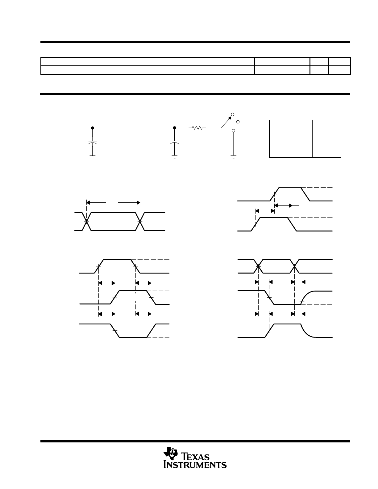
PARAMETER MEASUREMENT INFORMATION
From Output
Under Test
(see Note A)
LOAD CIRCUIT FOR
TOTEM-POLE OUTPUTS
Input
Test
Point
C
L
t
w
50% V
CC
VOLTAGE WAVEFORMS
PULSE DURATION
= 5 V, TA = 25°C
CC
PARAMETER TEST CONDITIONS TYP UNIT
V
CC
Open
GND
t
su
50% V
VOLTAGE WAVEFORMS
SETUP AND HOLD TIMES
t
t
Open Drain
50% V
CC
TEST S1
PLH/tPHL
t
PLZ/tPZL
PHZ/tPZH
CC
t
h
50% V
CC
Open
V
CC
GND
V
CC
From Output
Under Test
C
(see Note A)
50% V
L
LOAD CIRCUIT FOR
3-STATE AND OPEN-DRAIN OUTPUTS
V
CC
0 V
RL = 1 kΩ
CC
S1
Timing Input
Data Input
V
0 V
V
0 V
CC
CC
Input
t
PLH
In-Phase
Output
t
PHL
Out-of-Phase
Output
PROPAGATION DELAY TIMES
INVERTING AND NONINVERTING OUTPUTS
NOTES: A. CL includes probe and jig capacitance.
B. Waveform 1 is for an output with internal conditions such that the output is low except when disabled by the output control.
Waveform 2 is for an output with internal conditions such that the output is high except when disabled by the output control.
C. All input pulses are supplied by generators having the following characteristics: PRR ≤ 1 MHz, ZO = 50 Ω, tr ≤ 3 ns, tf ≤ 3 ns.
D. The outputs are measured one at a time with one input transition per measurement.
E. All parameters and waveforms are not applicable to all devices.
50% V
CC
50% V
50% V
VOLTAGE WAVEFORMS
50% V
CC
CC
Figure 1. Load Circuit and Voltage Waveforms
CC
t
PHL
50% V
t
PLH
50% V
CC
CC
V
0 V
V
V
V
V
CC
OH
OL
OH
OL
Output
Control
Output
Waveform 1
S1 at V
(see Note B)
Waveform 2
(see Note B)
CC
Output
S1 at GND
50% V
CC
t
PZL
50% V
t
PZH
50% V
VOLTAGE WAVEFORMS
ENABLE AND DISABLE TIMES
LOW- AND HIGH-LEVEL ENABLING
CC
CC
50% V
t
VOL + 0.3 V
t
VOH – 0.3 V
CC
PLZ
PHZ
V
CC
0 V
≈V
V
OL
V
OH
≈0 V
CC
POST OFFICE BOX 655303 • DALLAS, TEXAS 75265
5
Page 6
PACKAGE OPTION ADDENDUM
www.ti.com
18-Feb-2005
PACKAGING INFORMATION
Orderable Device Status
(1)
Package
Type
Package
Drawing
Pins Package
Qty
Eco Plan
SN74AHC139D ACTIVE SOIC D 16 40 Pb-Free
SN74AHC139DBLE OBSOLETE SSOP DB 16 None Call TI Call TI
SN74AHC139DBR ACTIVE SSOP DB 16 2000 Pb-Free
SN74AHC139DGVR ACTIVE TVSOP DGV 16 2000 Pb-Free
SN74AHC139DR ACTIVE SOIC D 16 2500 Pb-Free
SN74AHC139N ACTIVE PDIP N 16 25 Pb-Free
SN74AHC139NSR ACTIVE SO NS 16 2000 Pb-Free
SN74AHC139PW ACTIVE TSSOP PW 16 90 Pb-Free
SN74AHC139PWLE OBSOLETE TSSOP PW 16 None Call TI Call TI
SN74AHC139PWR ACTIVE TSSOP PW 16 2000 Pb-Free
SN74AHC139RGYR ACTIVE QFN RGY 16 1000 Green(RoHS &
no Sb/Br)
(1)
The marketing status values are defined as follows:
ACTIVE: Product device recommended for new designs.
LIFEBUY: TI has announced that the device will be discontinued, and a lifetime-buy period is in effect.
NRND: Not recommended for new designs. Device is in production to support existing customers, but TI does not recommend using this part in
a new design.
PREVIEW: Device has been announced but is not in production. Samples may or may not be available.
OBSOLETE: TI has discontinued the production of the device.
(RoHS)
(RoHS)
(RoHS)
(RoHS)
(RoHS)
(RoHS)
(RoHS)
(RoHS)
(2)
Lead/Ball Finish MSL Peak Temp
CU NIPDAU Level-2-260C-1 YEAR/
Level-1-235C-UNLIM
CU NIPDAU Level-2-260C-1 YEAR/
Level-1-235C-UNLIM
CU NIPDAU Level-1-250C-UNLIM
CU NIPDAU Level-2-260C-1 YEAR/
Level-1-235C-UNLIM
CU NIPDAU Level-NC-NC-NC
CU NIPDAU Level-2-260C-1 YEAR/
Level-1-235C-UNLIM
CU NIPDAU Level-1-250C-UNLIM
CU NIPDAU Level-1-250C-UNLIM
CU NIPDAU Level-2-260C-1YEAR
(3)
(2)
Eco Plan - May not be currently available - please check http://www.ti.com/productcontent for the latest availability information and additional
product content details.
None: Not yet available Lead (Pb-Free).
Pb-Free (RoHS): TI's terms "Lead-Free" or "Pb-Free" mean semiconductor products that are compatible with the current RoHS requirements
for all 6 substances, including the requirement that lead not exceed 0.1% by weight in homogeneous materials. Where designed to be soldered
at high temperatures, TI Pb-Free products are suitable for use in specified lead-free processes.
Green (RoHS & no Sb/Br): TI defines "Green" to mean "Pb-Free" and in addition, uses package materials that do not contain halogens,
including bromine (Br) or antimony (Sb) above 0.1% of total product weight.
(3)
MSL, Peak Temp. -- The Moisture Sensitivity Level rating according to the JEDECindustry standard classifications, and peak solder
temperature.
Important Information and Disclaimer:The information provided on this page represents TI's knowledge and belief as of the date that it is
provided. TI bases its knowledge and belief on information provided by third parties, and makes no representation or warranty as to the
accuracy of such information. Efforts are underway to better integrate information from third parties. TI has taken and continues to take
reasonable steps to provide representative and accurate information but may not have conducted destructive testing or chemical analysis on
incoming materials and chemicals. TI and TI suppliers consider certain information to be proprietary, and thus CAS numbers and other limited
information may not be available for release.
In no event shall TI's liability arising out of such information exceed the total purchase price of the TI part(s) at issue in this document sold by TI
to Customer on an annual basis.
Addendum-Page 1
Page 7
Page 8
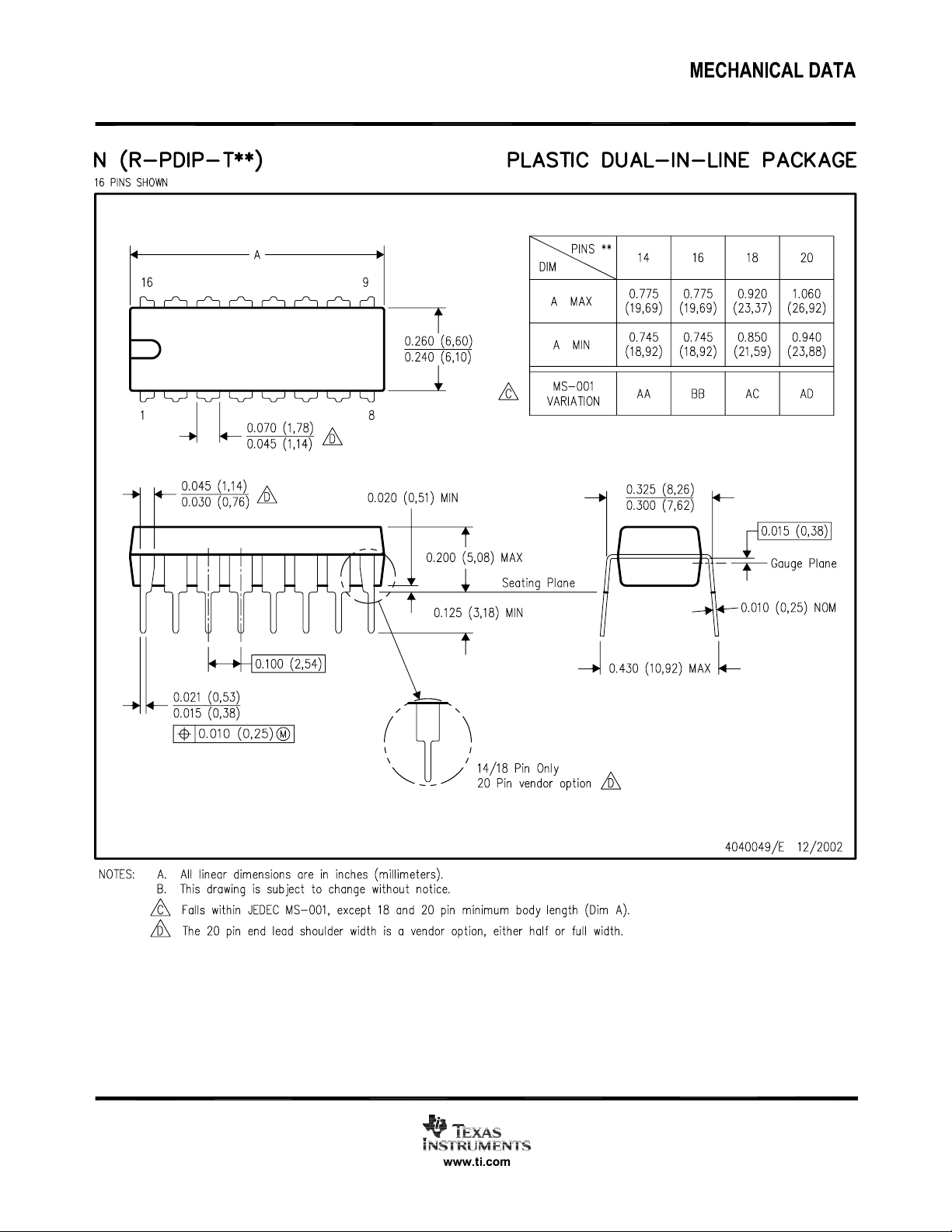
MECHANICAL DAT A
MPDS006C – FEBRUARY 1996 – REVISED AUGUST 2000
DGV (R-PDSO-G**) PLASTIC SMALL-OUTLINE
24 PINS SHOWN
0,40
24
112
A
0,23
0,13
13
0,07
4,50
4,30
M
6,60
6,20
0,16 NOM
Gage Plane
0,25
0°–8°
0,75
0,50
1,20 MAX
PINS **
DIM
A MAX
A MIN
NOTES: A. All linear dimensions are in millimeters.
B. This drawing is subject to change without notice.
C. Body dimensions do not include mold flash or protrusion, not to exceed 0,15 per side.
D. Falls within JEDEC: 24/48 Pins – MO-153
14/16/20/56 Pins – MO-194
0,15
0,05
14
3,70
3,50
Seating Plane
3,50
20
5,10
4,90
0,08
5,103,70
4,90
382416
7,90
7,70
48
9,80
9,60
56
11,40
11,20
4073251/E 08/00
POST OFFICE BOX 655303 • DALLAS, TEXAS 75265
Page 9

Page 10
Page 11
Page 12
MECHANICAL DATA
MSSO002E – JANUARY 1995 – REVISED DECEMBER 2001
DB (R-PDSO-G**) PLASTIC SMALL-OUTLINE
28 PINS SHOWN
0,65
28
1
2,00 MAX
0,38
0,22
15
14
A
0,05 MIN
0,15
M
5,60
5,00
Seating Plane
8,20
7,40
0,10
0,25
0,09
0°–ā8°
Gage Plane
0,25
0,95
0,55
PINS **
DIM
A MAX
A MIN
NOTES: A. All linear dimensions are in millimeters.
B. This drawing is subject to change without notice.
C. Body dimensions do not include mold flash or protrusion not to exceed 0,15.
D. Falls within JEDEC MO-150
14
6,50
6,50
5,905,90
2016
7,50
6,90
24
8,50
28
10,50
9,907,90
30
10,50
9,90
38
12,90
12,30
4040065 /E 12/01
POST OFFICE BOX 655303 • DALLAS, TEXAS 75265
Page 13

MECHANICAL DATA
MTSS001C – JANUARY 1995 – REVISED FEBRUARY 1999
PW (R-PDSO-G**) PLASTIC SMALL-OUTLINE PACKAGE
14 PINS SHOWN
0,65
1,20 MAX
14
0,30
0,19
8
4,50
4,30
PINS **
7
Seating Plane
0,15
0,05
8
1
A
DIM
14
0,10
6,60
6,20
M
0,10
0,15 NOM
0°–8°
2016
Gage Plane
24
0,25
0,75
0,50
28
A MAX
A MIN
NOTES: A. All linear dimensions are in millimeters.
B. This drawing is subject to change without notice.
C. Body dimensions do not include mold flash or protrusion not to exceed 0,15.
D. Falls within JEDEC MO-153
3,10
2,90
5,10
4,90
5,10
4,90
6,60
6,40
7,90
7,70
9,80
9,60
4040064/F 01/97
POST OFFICE BOX 655303 • DALLAS, TEXAS 75265
Page 14

IMPORTANT NOTICE
Texas Instruments Incorporated and its subsidiaries (TI) reserve the right to make corrections, modifications,
enhancements, improvements, and other changes to its products and services at any time and to discontinue
any product or service without notice. Customers should obtain the latest relevant information before placing
orders and should verify that such information is current and complete. All products are sold subject to TI’s terms
and conditions of sale supplied at the time of order acknowledgment.
TI warrants performance of its hardware products to the specifications applicable at the time of sale in
accordance with TI’s standard warranty. Testing and other quality control techniques are used to the extent TI
deems necessary to support this warranty . Except where mandated by government requirements, testing of all
parameters of each product is not necessarily performed.
TI assumes no liability for applications assistance or customer product design. Customers are responsible for
their products and applications using TI components. To minimize the risks associated with customer products
and applications, customers should provide adequate design and operating safeguards.
TI does not warrant or represent that any license, either express or implied, is granted under any TI patent right,
copyright, mask work right, or other TI intellectual property right relating to any combination, machine, or process
in which TI products or services are used. Information published by TI regarding third-party products or services
does not constitute a license from TI to use such products or services or a warranty or endorsement thereof.
Use of such information may require a license from a third party under the patents or other intellectual property
of the third party, or a license from TI under the patents or other intellectual property of TI.
Reproduction of information in TI data books or data sheets is permissible only if reproduction is without
alteration and is accompanied by all associated warranties, conditions, limitations, and notices. Reproduction
of this information with alteration is an unfair and deceptive business practice. TI is not responsible or liable for
such altered documentation.
Resale of TI products or services with statements different from or beyond the parameters stated by TI for that
product or service voids all express and any implied warranties for the associated TI product or service and
is an unfair and deceptive business practice. TI is not responsible or liable for any such statements.
Following are URLs where you can obtain information on other Texas Instruments products and application
solutions:
Products Applications
Amplifiers amplifier.ti.com Audio www.ti.com/audio
Data Converters dataconverter.ti.com Automotive www.ti.com/automotive
DSP dsp.ti.com Broadband www.ti.com/broadband
Interface interface.ti.com Digital Control www.ti.com/digitalcontrol
Logic logic.ti.com Military www.ti.com/military
Power Mgmt power.ti.com Optical Networking www.ti.com/opticalnetwork
Microcontrollers microcontroller.ti.com Security www.ti.com/security
Telephony www.ti.com/telephony
Video & Imaging www.ti.com/video
Wireless www.ti.com/wireless
Mailing Address: Texas Instruments
Post Office Box 655303 Dallas, Texas 75265
Copyright 2005, Texas Instruments Incorporated
 Loading...