

Page 1
查询5962-9231402QLA供应商
SN54ABT543A, SN74ABT543A
OCTAL REGISTERED TRANSCEIVERS
WITH 3-STATE OUTPUTS
SCBS157F – JANUARY 1991 – REVISED MA Y 1997
D
State-of-the-Art
EPIC-ΙΙB
BiCMOS Design
Significantly Reduces Power Dissipation
D
ESD Protection Exceeds 2000 V Per
MIL-STD-883, Method 3015; Exceeds 200 V
Using Machine Model (C = 200 pF, R = 0)
D
T ypical V
(Output Ground Bounce) < 1 V
OLP
at VCC = 5 V, TA = 25°C
D
High-Drive Outputs (–32-mA IOH, 64-mA IOL)
D
Package Options Include Plastic
Small-Outline (DW), Shrink Small-Outline
(DB), and Thin Shrink Small-Outline (PW)
Packages, Ceramic Chip Carriers (FK),
Ceramic Flat (W) Package, and Plastic (NT)
and Ceramic (JT) DIPs
description
The ’ABT543A octal transceivers contain two sets
of D-type latches for temporary storage of data
flowing in either direction. Separate latch-enable
(LEAB
or LEBA) and output-enable (OEAB or
OEBA) inputs are provided for each register to
permit independent control in either direction of
data flow.
The A-to-B enable (CEAB) input must be low to
enter data from A or to output data from B. If CEAB
is low and LEAB is low, the A-to-B latches are
transparent; a subsequent low-to-high transition
of LEAB
With CEAB and OEAB both low, the 3-state
B outputs are active and reflect the data present
at the output of the A latches. Data flow from B to
A is similar, but requires using the CEBA
and OEBA inputs.
T o ensure the high-impedance state during power
up or power down, OE should be tied to V
through a pullup resistor; the minimum value of
the resistor is determined by the current-sinking
capability of the driver.
puts the A latches in the storage mode.
, LEBA,
CC
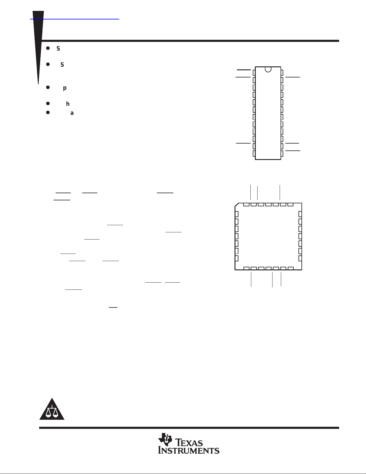
SN54ABT543A . . . JT OR W PACKAGE
SN74ABT543A . . . DB, DW, NT, OR PW PACKAGE
OEBA
CEAB
SN54ABT543A . . . FK PACKAGE
A2
A3
A4
NC
A5
A6
A7
NC – No internal connection
(TOP VIEW)
LEBA
GND
1
2
3
A1
A2
4
5
A3
A4
6
7
A5
8
A6
9
A7
10
A8
11
12
(TOP VIEW)
A1
OEBA
LEBANCCEBA
3212827
426
5
6
7
8
9
10
11
12 13
14 15 16 17 18
A8
GND
CEAB
NC
24
23
22
21
20
19
18
17
16
15
14
13
CC
V
OEAB
V
CC
CEBA
B1
B2
B3
B4
B5
B6
B7
B8
LEAB
OEAB
B1
25
24
23
22
21
20
19
B8
LEAB
B2
B3
B4
NC
B5
B6
B7
The SN54ABT543A is characterized for operation over the full military temperature range of –55°C to 125°C.
The SN74ABT543A is characterized for operation from –40°C to 85°C.
Please be aware that an important notice concerning availability, standard warranty, and use in critical applications of
Texas Instruments semiconductor products and disclaimers thereto appears at the end of this data sheet.
EPIC-ΙΙB is a trademark of Texas Instruments Incorporated.
PRODUCTION DATA information is current as of publication date.
Products conform to specifications per the terms of Texas Instruments
standard warranty. Production processing does not necessarily include
testing of all parameters.
POST OFFICE BOX 655303 • DALLAS, TEXAS 75265
Copyright 1997, Texas Instruments Incorporated
1
Page 2
SN54ABT543A, SN74ABT543A
OCTAL REGISTERED TRANSCEIVERS
WITH 3-STATE OUTPUTS
SCBS157F – JANUARY 1991 – REVISED MA Y 1997
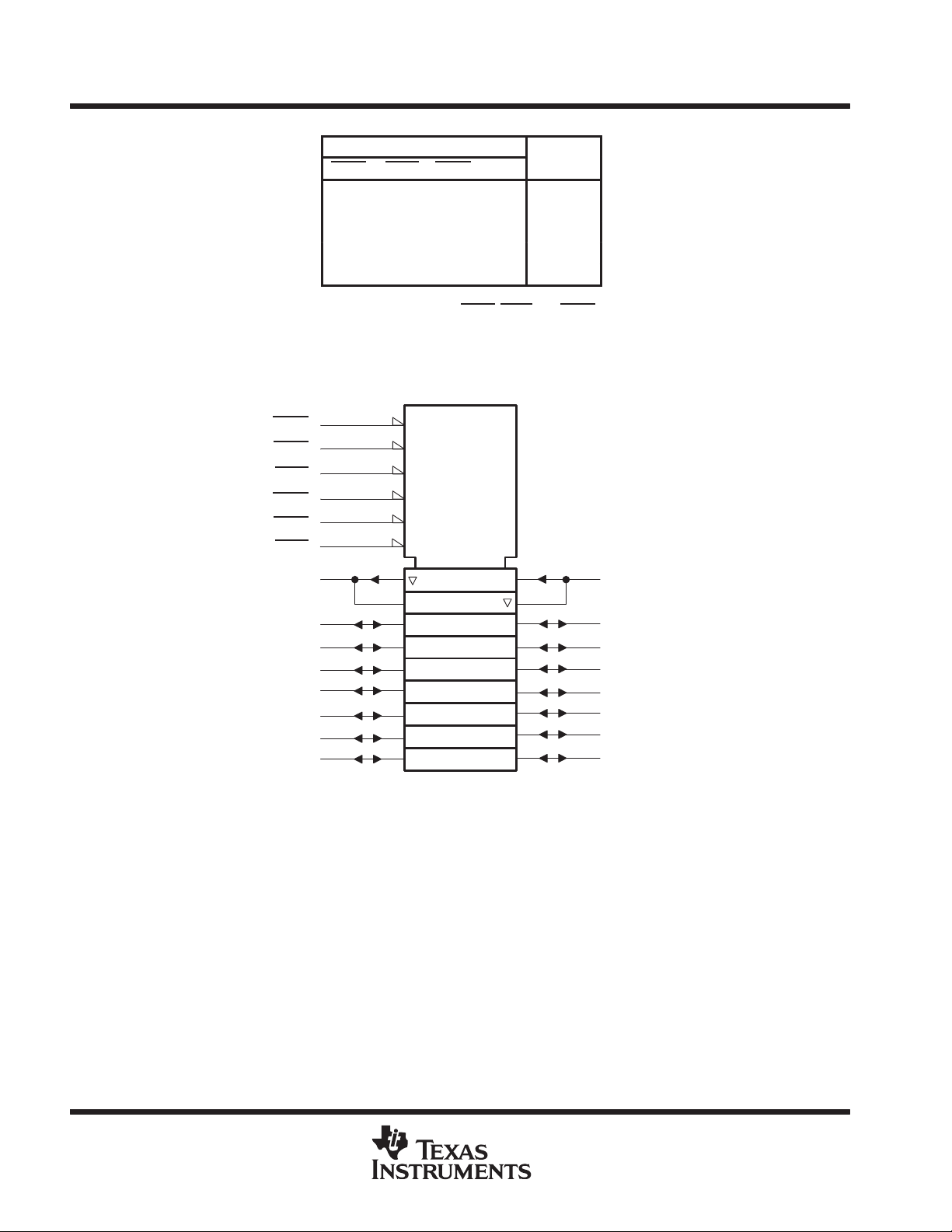
logic symbol
FUNCTION TABLE
INPUTS
CEAB LEAB OEAB A
H X X X Z
X XHX Z
L HLXB
L LLL L
L L L H H
†
A-to-B data flow is shown; B-to-A flow control is the
same except that it uses CEBA
‡
Output level before the indicated steady-state
input conditions were established
†
OUTPUT
B
‡
0
, LEBA, and OEBA.
§
A1
A2
A3
A4
A5
A6
A7
A8
2
23
1
13
11
14
3
4
5
6
7
8
9
10
1EN3
G1
1C5
2EN4
G2
2C6
3
6D
1
5D
1
4
22
21
20
19
18
17
16
15
B1
B2
B3
B4
B5
B6
B7
B8
OEBA
CEBA
LEBA
OEAB
CEAB
LEAB
§
This symbol is in accordance with ANSI/IEEE Std 91-1984 and IEC Publication 617-12.
Pin numbers shown are for the DB, DW, JT, NT, PW, and W packages.
2
POST OFFICE BOX 655303 • DALLAS, TEXAS 75265
Page 3
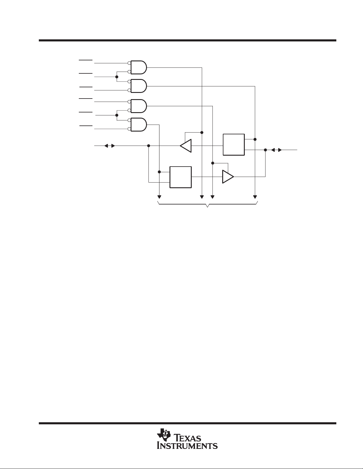
logic diagram (positive logic)
SN54ABT543A, SN74ABT543A
OCTAL REGISTERED TRANSCEIVERS
WITH 3-STATE OUTPUTS
SCBS157F – JANUARY 1991 – REVISED MA Y 1997
A1
2
23
1
13
11
14
3
C1
1D
To Seven Other Channels
OEBA
CEBA
LEBA
OEAB
CEAB
LEAB
Pin numbers shown are for the DB, DW, JT, NT, PW, and W packages.
C1
1D
22
B1
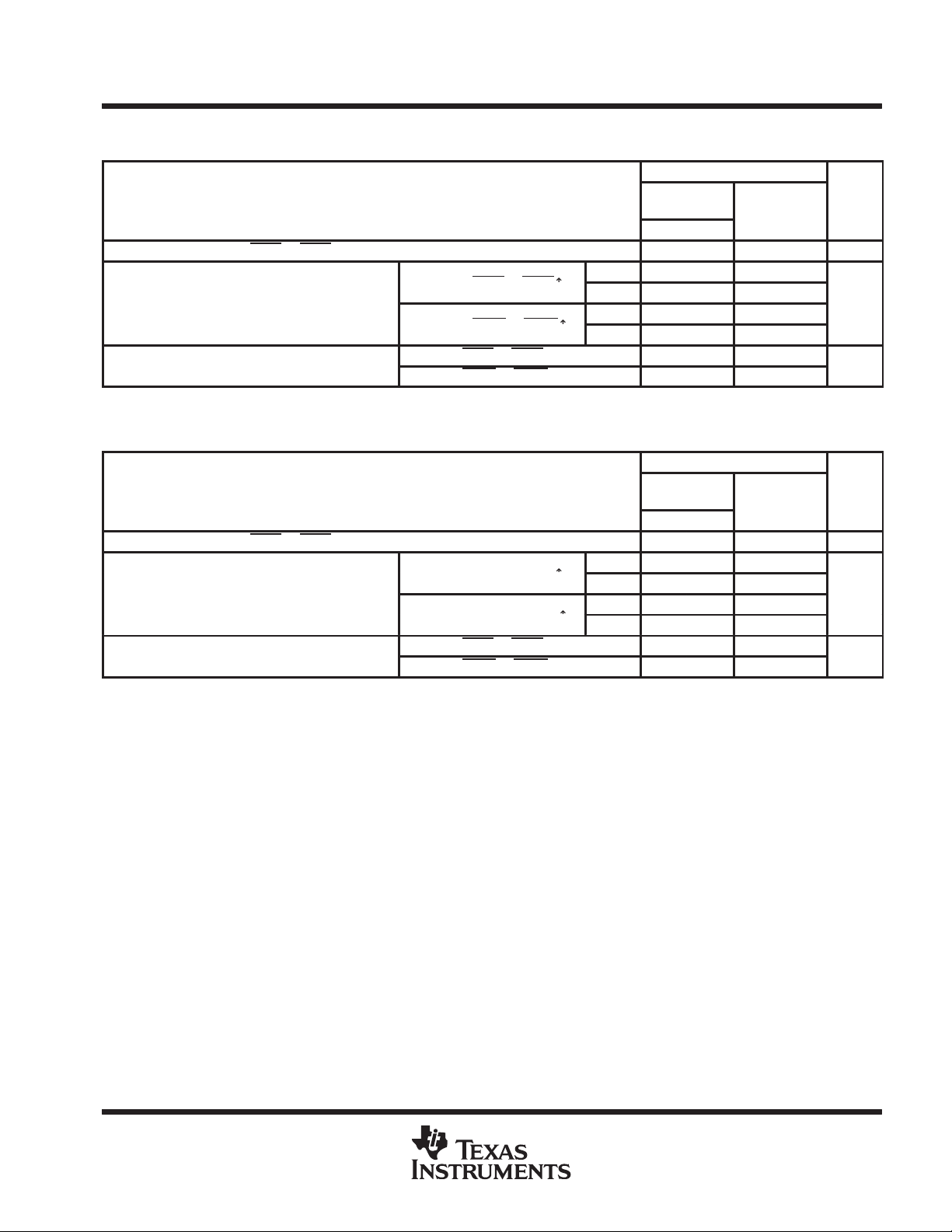
absolute maximum ratings over operating free-air temperature range (unless otherwise noted)
Supply voltage range, VCC –0.5 V to 7 V. . . . . . . . . . . . . . . . . . . . . . . . . . . . . . . . . . . . . . . . . . . . . . . . . . . . . . . . . .
Input voltage range, VI (except I/O ports) (see Note 1) –0.5 V to 7 V. . . . . . . . . . . . . . . . . . . . . . . . . . . . . . . . . .
Voltage range applied to any output in the high or power-off state, V
Current into any output in the low state, IO: SN54ABT543A 96 mA. . . . . . . . . . . . . . . . . . . . . . . . . . . . . . . . . . .
SN74ABT543A 128 mA. . . . . . . . . . . . . . . . . . . . . . . . . . . . . . . . . . .
Input clamp current, I
Output clamp current, I
Package thermal impedance, θ
(V
< 0) –18 mA. . . . . . . . . . . . . . . . . . . . . . . . . . . . . . . . . . . . . . . . . . . . . . . . . . . . . . . . . . .
IK
I
(V
< 0) –50 mA. . . . . . . . . . . . . . . . . . . . . . . . . . . . . . . . . . . . . . . . . . . . . . . . . . . . . . . .
OK
O
(see Note 2): DB package 104°C/W. . . . . . . . . . . . . . . . . . . . . . . . . . . . . . . .
JA
DW package 81°C/W. . . . . . . . . . . . . . . . . . . . . . . . . . . . . . . . .
NT package 67°C/W. . . . . . . . . . . . . . . . . . . . . . . . . . . . . . . . .
PW package 120°C/W. . . . . . . . . . . . . . . . . . . . . . . . . . . . . . . .
Storage temperature range, T
†
Stresses beyond those listed under “absolute maximum ratings” may cause permanent damage to the device. These are stress ratings only, and
functional operation of the device at these or any other conditions beyond those indicated under “recommended operating conditions” is not
implied. Exposure to absolute-maximum-rated conditions for extended periods may affect device reliability.
NOTES: 1. The input and output negative-voltage ratings may be exceeded if the input and output clamp-current ratings are observed.
2. The package thermal impedance is calculated in accordance with EIA/JEDEC Std JESD51, except for through-hole packages,
which use a trace length of zero.
–65°C to 150°C. . . . . . . . . . . . . . . . . . . . . . . . . . . . . . . . . . . . . . . . . . . . . . . . . . .
stg
–0.5 V to 5.5 V. . . . . . . . . . . . . . . . . . .
O
†
POST OFFICE BOX 655303 • DALLAS, TEXAS 75265
3
Page 4
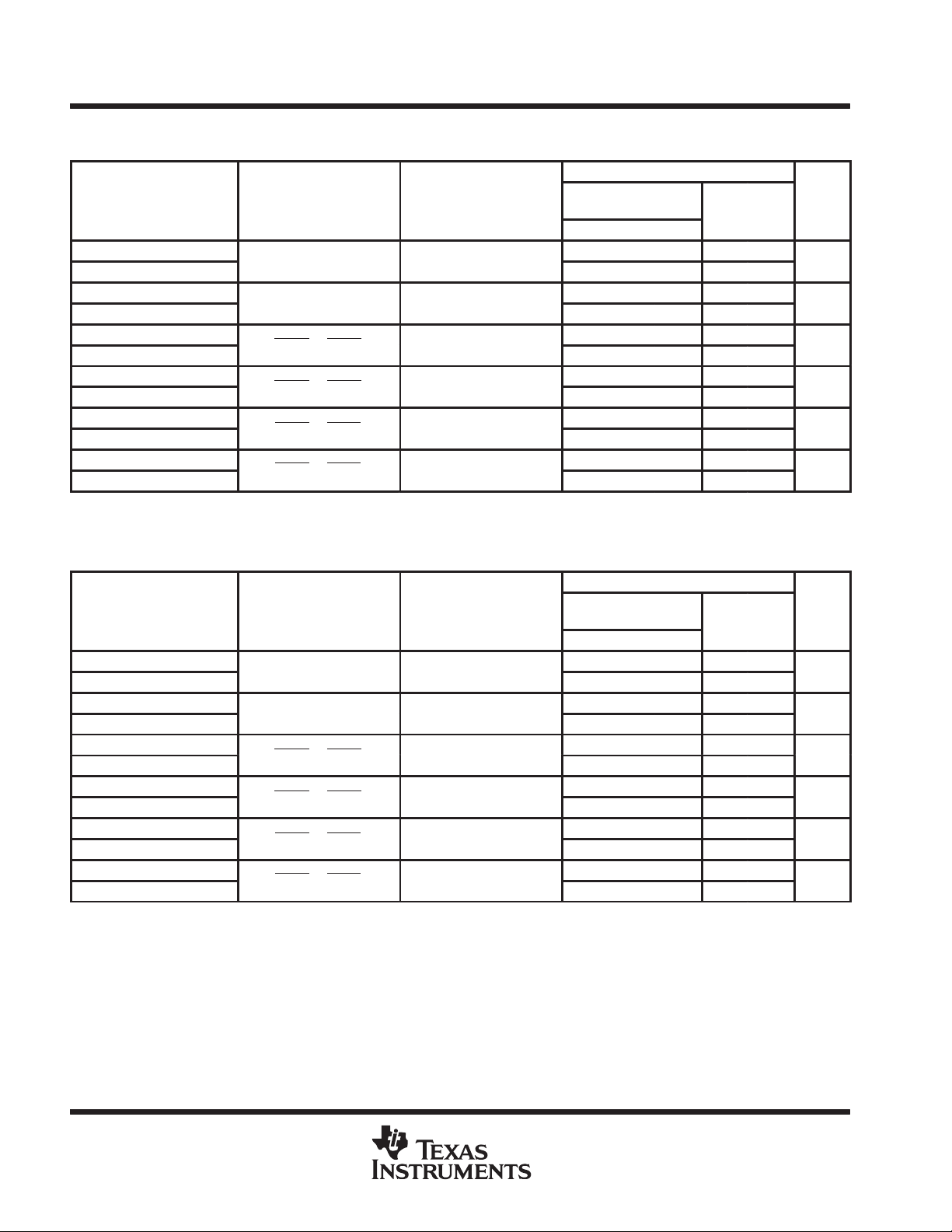
SN54ABT543A, SN74ABT543A
UNIT
PARAMETER
TEST CONDITIONS
UNIT
V
V
V
V
VOLV
4.5 V
V
I
V
V
V
GND
A
V
CC
OCTAL REGISTERED TRANSCEIVERS
WITH 3-STATE OUTPUTS
SCBS157F – JANUARY 1991 – REVISED MA Y 1997
recommended operating conditions (see Note 3)
SN54ABT543A SN74ABT543A
MIN MAX MIN MAX
V
V
V
V
I
OH
I
OL
∆t/∆v Input transition rise or fall rate Outputs enabled 5 5 ns/V
T
NOTE 3: Unused pins (input or I/O) must be held high or low to prevent them from floating.
electrical characteristics over recommended operating free-air temperature range (unless
otherwise noted)
V
V
I
I
OZH
I
OZL
I
off
I
CEX
I
O
I
CC
∆I
C
C
* On products compliant to MIL-PRF-38535, this parameter does not apply.
†
All typical values are at VCC = 5 V.
‡
The parameters I
§
This data sheet limit may vary among suppliers.
¶
Not more than one output should be tested at a time, and the duration of the test should not exceed one second.
#
This is the increase in supply current for each input that is at the specified TTL voltage level rather than VCC or GND.
Supply voltage 4.5 5.5 4.5 5.5 V
CC
High-level input voltage 2 2 V
IH
Low-level input voltage 0.8 0.8 V
IL
Input voltage 0 V
I
High-level output current –24 –32 mA
Low-level output current 48 64 mA
Operating free-air temperature –55 125 –40 85 °C
A
TA = 25°C SN54ABT543A SN74ABT543A
MIN TYP†MAX MIN MAX MIN MAX
IK
OH
hys
Control inputs
A or B ports
‡
‡
¶
A or B ports
#
CC
Control inputs VI = 2.5 V or 0.5 V 4 pF
i
A or B ports VO = 2.5 V or 0.5 V 7 pF
io
OZH
VCC = 4.5 V, II = –18 mA –1.2 –1.2 –1.2 V
VCC = 4.5 V, IOH = –3 mA 2.5 2.5 2.5
VCC = 5 V, IOH = –3 mA 3 3 3
= 4.5
CC
=
CC
= 5.5 V,
CC
VCC = 5.5 V, VO = 2.7 V 10
VCC = 5.5 V, VO = 0.5 V –10
VCC = 0, VI or VO ≤ 4.5 V ±100 ±100 µA
VCC = 5.5 V,
VO = 5.5 V
VCC = 5.5 V, VO = 2.5 V –50* –100 –180* –50 –200 –50 –180 mA
=
= 5.5 V,
IO = 0,
VI = VCC or GND
VCC = 5.5 V, One input at 3.4 V,
Other inputs at VCC or GND
and I
include the input leakage current.
OZL
IOH = –24 mA 2 2
IOH = –32 mA 2* 2
IOL = 48 mA 0.55 0.55
IOL = 64 mA 0.55* 0.55
100 mV
=
or
I
CC
Outputs high 50 50 50 µA
Outputs high 1 250* 350 250 µA
Outputs low 24 30* 34 30 mA
Outputs disabled 0.5 250* 350 250 µA
±1 ±1 ±1
±100 ±100 ±100
§
§
1.5 1.5 1.5 mA
10
–10
CC
§
§
0 V
10
–10
CC
V
µ
§
µA
§
µA
4
POST OFFICE BOX 655303 • DALLAS, TEXAS 75265
Page 5
Data bef
LEAB
LEBA↑
tsuSetup time
ns
Data bef
CEAB
CEBA↑
thHold time
ns
Data bef
LEAB
LEBA↑
tsuSetup time
ns
Data bef
CEAB
CEBA↑
thHold time
ns
SN54ABT543A, SN74ABT543A
OCTAL REGISTERED TRANSCEIVERS
WITH 3-STATE OUTPUTS
SCBS157F – JANUARY 1991 – REVISED MA Y 1997
timing requirements over recommended ranges of supply voltage and operating free-air
temperature (unless otherwise noted) (see Figure 1)
SN54ABT543A
VCC = 5 V,
TA = 25°C
MIN MAX
t
w
Pulse duration, LEAB or LEBA low 3.5 3.5 ns
ore
p
ore
Data after LEAB or LEBA↑ 1 1
Data after CEAB or CEBA↑ 1 1
or
or
High 2.5 2.5
Low 3 3
High 2.5 2.5
Low 3 3
MIN MAX
timing requirements over recommended ranges of supply voltage and operating free-air
temperature (unless otherwise noted) (see Figure 1)
SN74ABT543A
VCC = 5 V,
TA = 25°C
MIN MAX
t
w
Pulse duration, LEAB or LEBA low 3.5 3.5 ns
ore
p
ore
Data after LEAB or LEBA↑ 0.5 0.5
Data after CEAB or CEBA↑ 0.5 0.5
or
or
High 3.5 3.5
Low 3 3
High 3.5 3.5
Low 3 3
MIN MAX
UNIT
UNIT
POST OFFICE BOX 655303 • DALLAS, TEXAS 75265
5
Page 6
SN54ABT543A, SN74ABT543A
A or B
B or A
ns
LEBA
LEAB
A or B
ns
OEBA
OEAB
A or B
ns
OEBA
OEAB
A or B
ns
CEBA
CEAB
A or B
ns
CEBA or CEAB
A or B
ns
A or B
B or A
ns
LEBA
LEAB
A or B
ns
OEBA
OEAB
A or B
ns
OEBA
OEAB
A or B
ns
CEBA
CEAB
A or B
ns
CEBA or CEAB
A or B
ns
OCTAL REGISTERED TRANSCEIVERS
WITH 3-STATE OUTPUTS
SCBS157F – JANUARY 1991 – REVISED MA Y 1997
switching characteristics over recommended ranges of supply voltage and operating free-air
temperature, C
PARAMETER
t
PLH
t
PHL
t
PLH
t
PHL
t
PZH
t
PZL
t
PHZ
t
PLZ
t
PZH
t
PZL
t
PHZ
t
†
This data sheet limit may vary among suppliers.
PLZ
= 50 pF (unless otherwise noted) (see Figure 1)
L
FROM
(INPUT)
or
or
or
or
TO
(OUTPUT)
SN54ABT543A
VCC = 5 V,
TA = 25°C
MIN TYP MAX
†
1.6
1.6
2.5
2.5
3.2†
2.5
4.4 4.4 1.6
1.6 4.4 5.1 1.6 6.2
†
4.1 5.1 1.6
1.6 4.6 5.4 1.6 6.4
1.4 3.9 4.1 1.4 5.1
2 5 4.9 2 5.8
†
5.9 5.8 2.5
†
5.5 6.1 2.5
1.4 3.9 4.7 1.4 5.6
2 5 5.7 2 6.2
5.9 6.5
†
5.5 6.7 2.5
MIN MAX
†
†
†
†
3.2†
†
UNIT
5.5
6.6
6.9
7.6
7.3
7.8
switching characteristics over recommended ranges of supply voltage and operating free-air
temperature, C
PARAMETER
t
PLH
t
PHL
t
PLH
t
PHL
t
PZH
t
PZL
t
PHZ
t
PLZ
t
PZH
t
PZL
t
PHZ
t
†
This data sheet limit may vary among suppliers.
PLZ
= 50 pF (unless otherwise noted) (see Figure 1)
L
FROM
(INPUT)
or
or
or
or
TO
(OUTPUT)
SN74ABT543A
VCC = 5 V,
TA = 25°C
MIN TYP MAX
†
1.8
1.5
2.5
2.5
2.9†
2.4
4.4 5.9 1.8
1.9 4.4 5.9 1.9 6.9
†
4.1 5.6 1.5
2.1 4.6 6.1 2.1 7.1
1.4 3.9 5.4 1.4 6.4
2.5 5 6.5 2.5 7.5
†
5.9 7.4 2.5
†
5.5 7 2.5
1.4 3.9 5.4 1.4 6.4
2.5 5 6.5 2.5 7.5
5.9 7.4
†
5.5 7 2.4
MIN MAX
†
†
†
†
2.9†
†
UNIT
6.9
6.6
8.4
8
8.4
8
6
POST OFFICE BOX 655303 • DALLAS, TEXAS 75265
Page 7
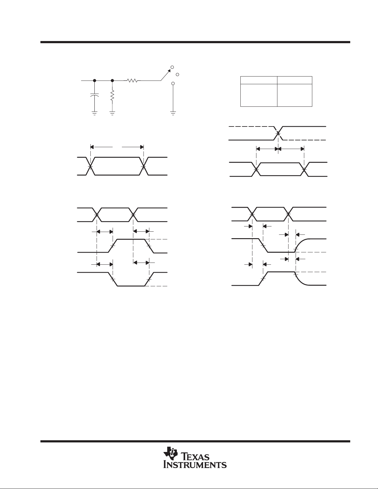
From Output
Under Test
CL = 50 pF
(see Note A)
SN54ABT543A, SN74ABT543A
OCTAL REGISTERED TRANSCEIVERS
SCBS157F – JANUARY 1991 – REVISED MA Y 1997
PARAMETER MEASUREMENT INFORMATION
7 V
500 Ω
500 Ω
S1
Open
GND
TEST S1
t
PLH/tPHL
t
PLZ/tPZL
t
PHZ/tPZH
WITH 3-STATE OUTPUTS
Open
7 V
Open
LOAD CIRCUIT
t
w
Input
Input
Output
Output
INVERTING AND NONINVERTING OUTPUTS
1.5 V 1.5 V
VOLTAGE WAVEFORMS
PULSE DURATION
1.5 V 1.5 V
t
PLH
1.5 V
t
PHL
VOLTAGE WAVEFORMS
PROPAGATION DELAY TIMES
t
PHL
1.5 V
t
1.5 V1.5 V
PLH
3 V
0 V
3 V
0 V
V
V
V
V
OH
OL
OH
OL
Timing Input
Data Input
Output
Control
Output
Waveform 1
S1 at 7 V
(see Note B)
Output
Waveform 2
S1 at Open
(see Note B)
1.5 V
t
su
1.5 V 1.5 V
VOLTAGE WAVEFORMS
SETUP AND HOLD TIMES
1.5 V
t
PZL
t
PLZ
1.5 V
t
t
PZH
ENABLE AND DISABLE TIMES
LOW- AND HIGH-LEVEL ENABLING
PHZ
1.5 V
VOLTAGE WAVEFORMS
t
h
1.5 V
VOL + 0.3 V
VOH – 0.3 V
3 V
0 V
3 V
0 V
3 V
0 V
3.5 V
V
OL
V
OH
≈ 0 V
NOTES: A. CL includes probe and jig capacitance.
B. Waveform 1 is for an output with internal conditions such that the output is low except when disabled by the output control.
Waveform 2 is for an output with internal conditions such that the output is high except when disabled by the output control.
C. All input pulses are supplied by generators having the following characteristics: PRR ≤ 10 MHz, ZO = 50 Ω, tr ≤ 2.5 ns, tf≤ 2.5 ns.
D. The outputs are measured one at a time with one transition per measurement.
Figure 1. Load Circuit and Voltage Waveforms
POST OFFICE BOX 655303 • DALLAS, TEXAS 75265
7
Page 8

PACKAGE OPTION ADDENDUM
www.ti.com
26-Sep-2005
PACKAGING INFORMATION
Orderable Device Status
(1)
Package
Type
Package
Drawing
Pins Package
Qty
Eco Plan
5962-9231402Q3A ACTIVE LCCC FK 28 1 TBD Call TI Level-NC-NC-NC
5962-9231402QKA ACTIVE CFP W 24 1 TBD Call TI Level-NC-NC-NC
5962-9231402QLA ACTIVE CDIP JT 24 1 TBD Call TI Level-NC-NC-NC
SN74ABT543ADBLE OBSOLETE SSOP DB 24 TBD Call TI Call TI
SN74ABT543ADBR ACTIVE SSOP DB 24 2000 Green (RoHS &
no Sb/Br)
SN74ABT543ADBRE4 ACTIVE SSOP DB 24 2000 Green (RoHS &
no Sb/Br)
SN74ABT543ADW ACTIVE SOIC DW 24 25 Green (RoHS &
no Sb/Br)
SN74ABT543ADWE4 ACTIVE SOIC DW 24 25 Green (RoHS &
no Sb/Br)
SN74ABT543ADWR ACTIVE SOIC DW 24 2000 Green (RoHS &
no Sb/Br)
SN74ABT543ADWRE4 ACTIVE SOIC DW 24 2000 Green (RoHS &
no Sb/Br)
SN74ABT543ANSR ACTIVE SO NS 24 2000 Green (RoHS &
no Sb/Br)
SN74ABT543ANSRE4 ACTIVE SO NS 24 2000 Green (RoHS &
no Sb/Br)
SN74ABT543ANT ACTIVE PDIP NT 24 15 Pb-Free
SN74ABT543ANTE4 ACTIVE PDIP NT 24 15 Pb-Free
SN74ABT543APW ACTIVE TSSOP PW 24 60 Green (RoHS &
no Sb/Br)
SN74ABT543APWE4 ACTIVE TSSOP PW 24 60 Green (RoHS &
no Sb/Br)
SN74ABT543APWLE OBSOLETE TSSOP PW 24 TBD Call TI Call TI
SN74ABT543APWR ACTIVE TSSOP PW 24 2000 Green (RoHS &
no Sb/Br)
SN74ABT543APWRE4 ACTIVE TSSOP PW 24 2000 Green (RoHS &
no Sb/Br)
SNJ54ABT543AFK ACTIVE LCCC FK 28 1 TBD CallTI Level-NC-NC-NC
SNJ54ABT543AJT ACTIVE CDIP JT 24 1 TBD Call TI Level-NC-NC-NC
SNJ54ABT543AW ACTIVE CFP W 24 1 TBD Call TI Level-NC-NC-NC
(1)
The marketing status values are defined as follows:
ACTIVE: Product device recommended for new designs.
LIFEBUY: TI has announced that the device will be discontinued, and a lifetime-buy period is in effect.
NRND: Not recommended for new designs. Device is in production to support existing customers, but TI does not recommend using this part in
a new design.
PREVIEW: Device has been announced but is not in production. Samples may or may not be available.
OBSOLETE: TI has discontinued the production of the device.
(RoHS)
(RoHS)
(2)
Lead/Ball Finish MSL Peak Temp
CU NIPD Level-1-260C-UNLIM
CU NIPD Level-1-260C-UNLIM
CU NIPDAU Level-1-260C-UNLIM
CU NIPDAU Level-1-260C-UNLIM
CU NIPDAU Level-1-260C-UNLIM
CU NIPDAU Level-1-260C-UNLIM
CU NIPDAU Level-1-260C-UNLIM
CU NIPDAU Level-1-260C-UNLIM
CU NIPDAU Level-NC-NC-NC
CU NIPDAU Level-NC-NC-NC
CU NIPDAU Level-1-260C-UNLIM
CU NIPDAU Level-1-260C-UNLIM
CU NIPDAU Level-1-260C-UNLIM
CU NIPDAU Level-1-260C-UNLIM
(3)
(2)
Eco Plan - The planned eco-friendly classification: Pb-Free (RoHS) or Green (RoHS & no Sb/Br) - please check
http://www.ti.com/productcontent for the latest availability information and additional product content details.
TBD: The Pb-Free/Green conversion plan has not been defined.
Pb-Free (RoHS): TI's terms "Lead-Free" or "Pb-Free" mean semiconductor products that are compatible with the current RoHS requirements
for all 6 substances, including the requirement that lead not exceed 0.1% by weight in homogeneous materials. Where designed to be soldered
Addendum-Page 1
Page 9

PACKAGE OPTION ADDENDUM
www.ti.com
at high temperatures, TI Pb-Free products are suitable for use in specified lead-free processes.
Green (RoHS & no Sb/Br): TI defines "Green" to mean Pb-Free (RoHS compatible), and free of Bromine (Br) and Antimony (Sb) based flame
retardants (Br or Sb do not exceed 0.1% by weight in homogeneous material)
(3)
MSL, Peak Temp. -- The Moisture Sensitivity Level rating according to the JEDEC industry standard classifications, and peak solder
temperature.
Important Information and Disclaimer:The information provided on this page represents TI's knowledge and belief as of the date that it is
provided. TI bases its knowledge and belief on information provided by third parties, and makes no representation or warranty as to the
accuracy of such information. Efforts are underway to better integrate information from third parties. TI has taken and continues to take
reasonable steps to provide representative and accurate information but may not have conducted destructive testing or chemical analysis on
incoming materials and chemicals. TI and TI suppliers consider certain information to be proprietary, and thus CAS numbers and other limited
information may not be available for release.
In no event shall TI's liability arising out of such information exceed the total purchase price of the TI part(s) at issue in this document sold by TI
to Customer on an annual basis.
26-Sep-2005
Addendum-Page 2
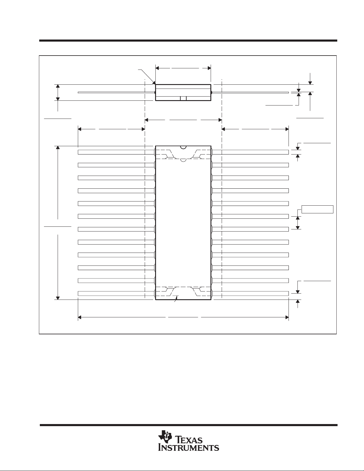
Page 10

MECHANICAL DATA
MCER004A – JANUARY 1995 – REVISED JANUARY 1997
JT (R-GDIP-T**) CERAMIC DUAL-IN-LINE
24 LEADS SHOWN
24
1
0.100 (2,54) MAX
0.070 (1,78)
0.030 (0,76)
0.023 (0,58)
0.015 (0,38)
A
13
B
12
0.015 (0,38) MIN
0.200 (5,08) MAX
Seating Plane
0.130 (3,30) MIN
DIM
A MAX
A MIN
B MAX
B MIN
PINS **
24
1.280
(32,51)
1.240
(31,50)
0.300
(7,62)
0.245
(6,22)
0.320 (8,13)
0.290 (7,37)
0°–15°
28
1.460
(37,08)
1.440
(36,58)
0.291
(7,39)
0.285
(7,24)
0.100 (2,54)
NOTES: A. All linear dimensions are in inches (millimeters).
B. This drawing is subject to change without notice.
C. This package can be hermetically sealed with a ceramic lid using glass frit.
D. Index point is provided on cap for terminal identification.
E. Falls within MIL STD 1835 GDIP3-T24, GDIP4-T28, and JEDEC MO-058 AA, MO-058 AB
0.014 (0,36)
0.008 (0,20)
4040110/C 08/96
POST OFFICE BOX 655303 • DALLAS, TEXAS 75265
Page 11
MECHANICAL DATA
MCFP007 – OCTOBER 1994
W (R-GDFP-F24) CERAMIC DUAL FLATPACK
0.090 (2,29)
0.045 (1,14)
0.640 (16,26)
0.490 (12,45)
Base and Seating Plane
0.360 (9,14)
0.240 (6,10)
0.375 (9,53)
0.340 (8,64)
0.006 (0,15)
0.004 (0,10)
0.395 (10,03)
0.360 (9,14)
124
0.360 (9,14)
0.240 (6,10)
0.045 (1,14)
0.026 (0,66)
0.019 (0,48)
0.015 (0,38)
0.050 (1,27)
30° TYP
NOTES: A. All linear dimensions are in inches (millimeters).
B. This drawing is subject to change without notice.
C. This package can be hermetically sealed with a ceramic lid using glass frit.
D. Falls within MIL-STD-1835 GDFP2-F24 and JEDEC MO-070AD
E. Index point is provided on cap for terminal identification only.
0.030 (0,76)
0.015 (0,38)
1312
1.115 (28,32)
0.840 (21,34)
4040180-5/B 03/95
POST OFFICE BOX 655303 • DALLAS, TEXAS 75265
Page 12

MECHANICAL DATA
MLCC006B – OCTOBER 1996
FK (S-CQCC-N**) LEADLESS CERAMIC CHIP CARRIER
28 TERMINAL SHOWN
A SQ
B SQ
19
20
21
22
23
24
25
12826 27
12
1314151618 17
0.020 (0,51)
0.010 (0,25)
MIN
0.342
(8,69)
0.442
0.640
0.739
0.938
1.141
A
0.358
(9,09)
0.458
(11,63)
0.660
(16,76)
0.761
(19,32)(18,78)
0.962
(24,43)
1.165
(29,59)
NO. OF
TERMINALS
**
11
10
9
8
7
6
5
432
20
28
44
52
68
84
0.020 (0,51)
0.010 (0,25)
(11,23)
(16,26)
(23,83)
(28,99)
MINMAX
0.307
(7,80)
0.406
(10,31)
0.495
(12,58)
0.495
(12,58)
0.850
(21,6)
1.047
(26,6)
0.080 (2,03)
0.064 (1,63)
B
MAX
0.358
(9,09)
0.458
(11,63)
0.560
(14,22)
0.560
(14,22)
0.858
(21,8)
1.063
(27,0)
0.055 (1,40)
0.045 (1,14)
0.028 (0,71)
0.022 (0,54)
0.050 (1,27)
NOTES: A. All linear dimensions are in inches (millimeters).
B. This drawing is subject to change without notice.
C. This package can be hermetically sealed with a metal lid.
D. The terminals are gold plated.
E. Falls within JEDEC MS-004
POST OFFICE BOX 655303 • DALLAS, TEXAS 75265
0.045 (1,14)
0.035 (0,89)
0.045 (1,14)
0.035 (0,89)
4040140/D 10/96
Page 13

MECHANICAL DATA
MPDI004 – OCTOBER 1994
NT (R-PDIP-T**) PLASTIC DUAL-IN-LINE PACKAGE
24 PINS SHOWN
24
DIM
A MAX
A MIN
B MAX
B MIN
PINS **
24
1.260
(32,04)
1.230
(31,24)
0.310
(7,87)
0.290
(7,37)
0°–15°
28
1.425
(36,20)
1.385
(35,18)
0.315
(8,00)
0.295
(7,49)
B
A
13
0.280 (7,11)
0.250 (6,35)
1
0.070 (1,78) MAX
0.020 (0,51) MIN
0.100 (2,54)
0.021 (0,53)
0.015 (0,38)
0.010 (0,25)
M
12
0.200 (5,08) MAX
Seating Plane
0.125 (3,18) MIN
0.010 (0,25) NOM
NOTES: A. All linear dimensions are in inches (millimeters).
B. This drawing is subject to change without notice.
4040050/B 04/95
POST OFFICE BOX 655303 • DALLAS, TEXAS 75265
Page 14

Page 15
Page 16
MECHANICAL DATA
MSSO002E – JANUARY 1995 – REVISED DECEMBER 2001
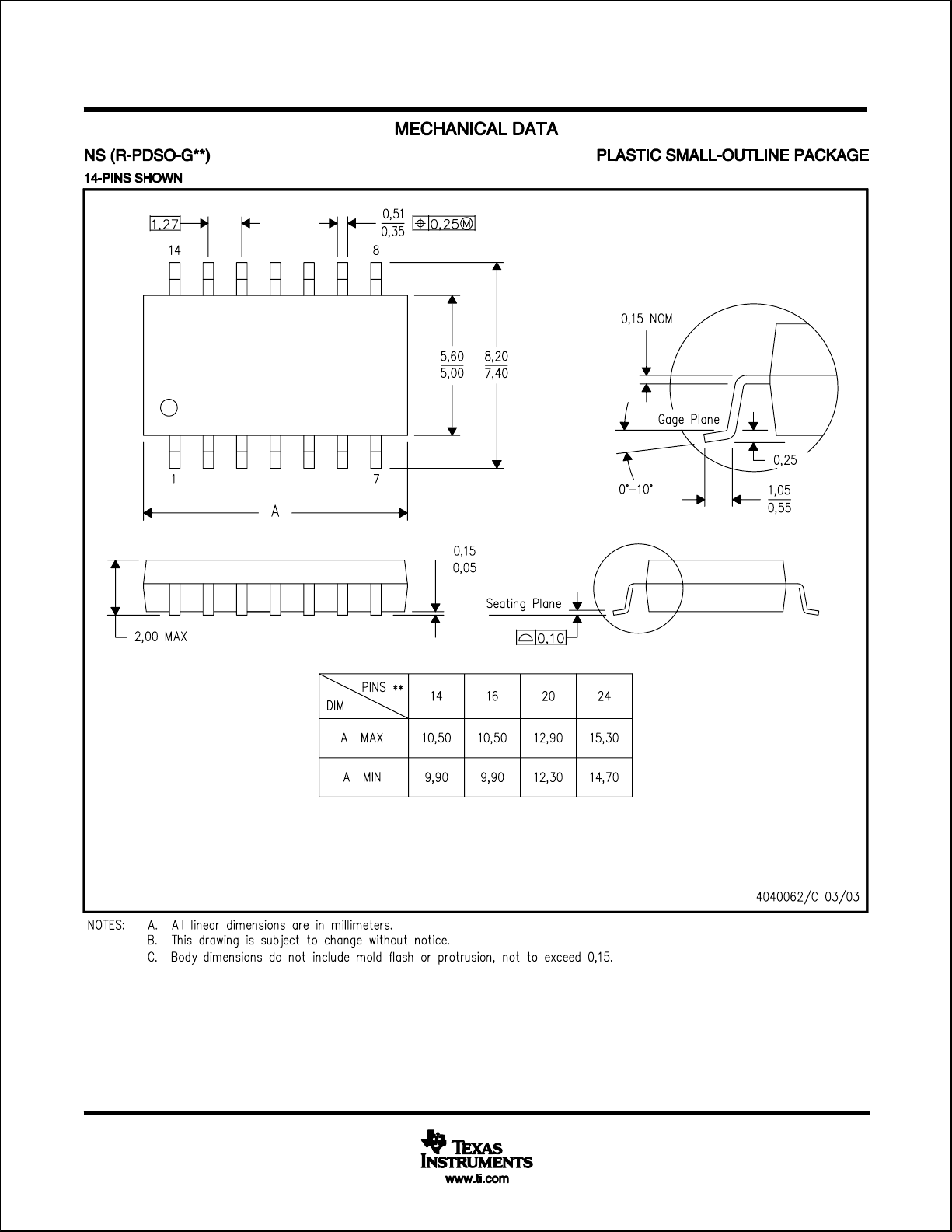
DB (R-PDSO-G**) PLASTIC SMALL-OUTLINE
28 PINS SHOWN
0,65
28
1
2,00 MAX
0,38
0,22
15
14
A
0,05 MIN
0,15
5,60
5,00
M
8,20
7,40
Seating Plane
0,10
0,25
0,09
0°–ā8°
Gage Plane
0,25
0,95
0,55
PINS **
DIM
A MAX
A MIN
NOTES: A. All linear dimensions are in millimeters.
B. This drawing is subject to change without notice.
C. Body dimensions do not include mold flash or protrusion not to exceed 0,15.
D. Falls within JEDEC MO-150
14
6,50
6,50
5,905,90
2016
7,50
6,90
24
8,50
28
10,50
9,907,90
30
10,50
9,90
38
12,90
12,30
4040065 /E 12/01
POST OFFICE BOX 655303 • DALLAS, TEXAS 75265
Page 17
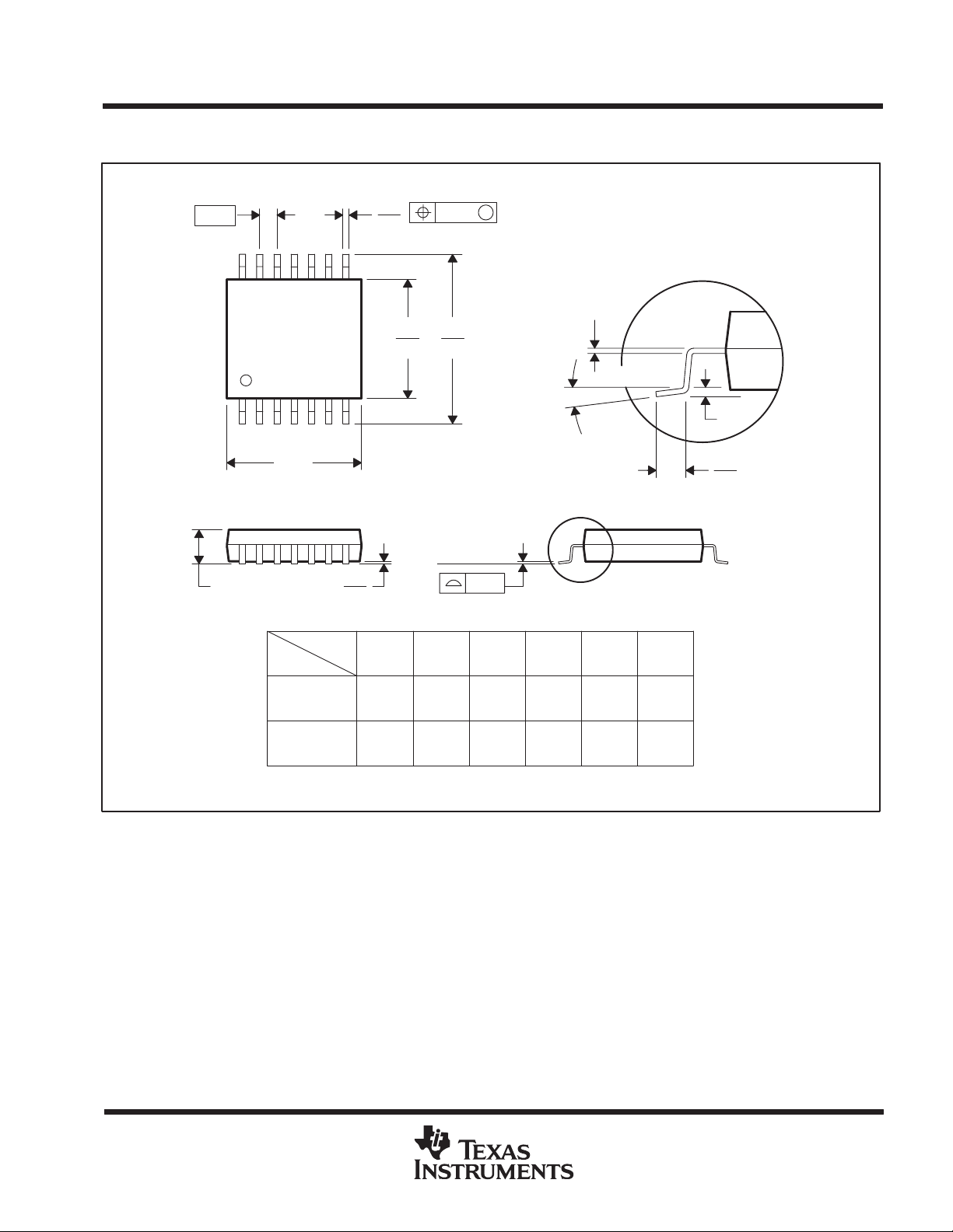
MECHANICAL DATA
MTSS001C – JANUARY 1995 – REVISED FEBRUARY 1999
PW (R-PDSO-G**) PLASTIC SMALL-OUTLINE PACKAGE
14 PINS SHOWN
0,65
1,20 MAX
14
0,30
0,19
8
4,50
4,30
PINS **
7
Seating Plane
0,15
0,05
8
1
A
DIM
6,60
6,20
14
0,10
M
0,10
0,15 NOM
0°–8°
2016
Gage Plane
24
0,25
0,75
0,50
28
A MAX
A MIN
NOTES: A. All linear dimensions are in millimeters.
B. This drawing is subject to change without notice.
C. Body dimensions do not include mold flash or protrusion not to exceed 0,15.
D. Falls within JEDEC MO-153
3,10
2,90
5,10
4,90
5,10
4,90
6,60
6,40
7,90
7,70
9,80
9,60
4040064/F 01/97
POST OFFICE BOX 655303 • DALLAS, TEXAS 75265
Page 18

IMPORTANT NOTICE
Texas Instruments Incorporated and its subsidiaries (TI) reserve the right to make corrections, modifications,
enhancements, improvements, and other changes to its products and services at any time and to discontinue
any product or service without notice. Customers should obtain the latest relevant information before placing
orders and should verify that such information is current and complete. All products are sold subject to TI’s terms
and conditions of sale supplied at the time of order acknowledgment.
TI warrants performance of its hardware products to the specifications applicable at the time of sale in
accordance with TI’s standard warranty. Testing and other quality control techniques are used to the extent TI
deems necessary to support this warranty . Except where mandated by government requirements, testing of all
parameters of each product is not necessarily performed.
TI assumes no liability for applications assistance or customer product design. Customers are responsible for
their products and applications using TI components. To minimize the risks associated with customer products
and applications, customers should provide adequate design and operating safeguards.
TI does not warrant or represent that any license, either express or implied, is granted under any TI patent right,
copyright, mask work right, or other TI intellectual property right relating to any combination, machine, or process
in which TI products or services are used. Information published by TI regarding third-party products or services
does not constitute a license from TI to use such products or services or a warranty or endorsement thereof.
Use of such information may require a license from a third party under the patents or other intellectual property
of the third party, or a license from TI under the patents or other intellectual property of TI.
Reproduction of information in TI data books or data sheets is permissible only if reproduction is without
alteration and is accompanied by all associated warranties, conditions, limitations, and notices. Reproduction
of this information with alteration is an unfair and deceptive business practice. TI is not responsible or liable for
such altered documentation.
Resale of TI products or services with statements different from or beyond the parameters stated by TI for that
product or service voids all express and any implied warranties for the associated TI product or service and
is an unfair and deceptive business practice. TI is not responsible or liable for any such statements.
Following are URLs where you can obtain information on other Texas Instruments products and application
solutions:
Products Applications
Amplifiers amplifier.ti.com Audio www.ti.com/audio
Data Converters dataconverter.ti.com Automotive www.ti.com/automotive
DSP dsp.ti.com Broadband www.ti.com/broadband
Interface interface.ti.com Digital Control www.ti.com/digitalcontrol
Logic logic.ti.com Military www.ti.com/military
Power Mgmt power.ti.com Optical Networking www.ti.com/opticalnetwork
Microcontrollers microcontroller.ti.com Security www.ti.com/security
Telephony www.ti.com/telephony
Video & Imaging www.ti.com/video
Wireless www.ti.com/wireless
Mailing Address: Texas Instruments
Post Office Box 655303 Dallas, Texas 75265
Copyright 2005, Texas Instruments Incorporated
 Loading...