

Page 1
SN54273, SN54LS273, SN74273, SN74LS273
OCTAL D-TYPE FLIP-FLOP WITH CLEAR
SDLS090 – OCTOBER 1976 – REVISED MARCH 1988
• Contains Eight Flip-Flops With Single-Rail
Outputs
• Buffered Clock and Direct Clear Inputs
• Individual Data Input to Each Flip-Flop
• Applications Include:
Buffer/Storage Registers
Shift Registers
description
Pattern Generators
These monolithic, positive-edge-triggered flipflops utilize TTL circuitry to implement D-type
flip-flop logic with a direct clear input.
Information at the D inputs meeting the setup time
requirements is transferred to the Q outputs on the
positive-going edge of the clock pulse. Clock
triggering occurs at a particular voltage level and
is not directly related to the transition time of the
positive-going pulse. When the clock input is at
either the high or low level, the D input signal has
no effect ar the output.
These flip-flops are guaranteed to respond to
clock frequencies ranging form 0 to 30 megahertz
while maximum clock frequency is typically 40
megahertz. Typical power dissipation is 39
milliwatts per flip-flop for the ′273 and 10 milliwatts
for the ′LS273.
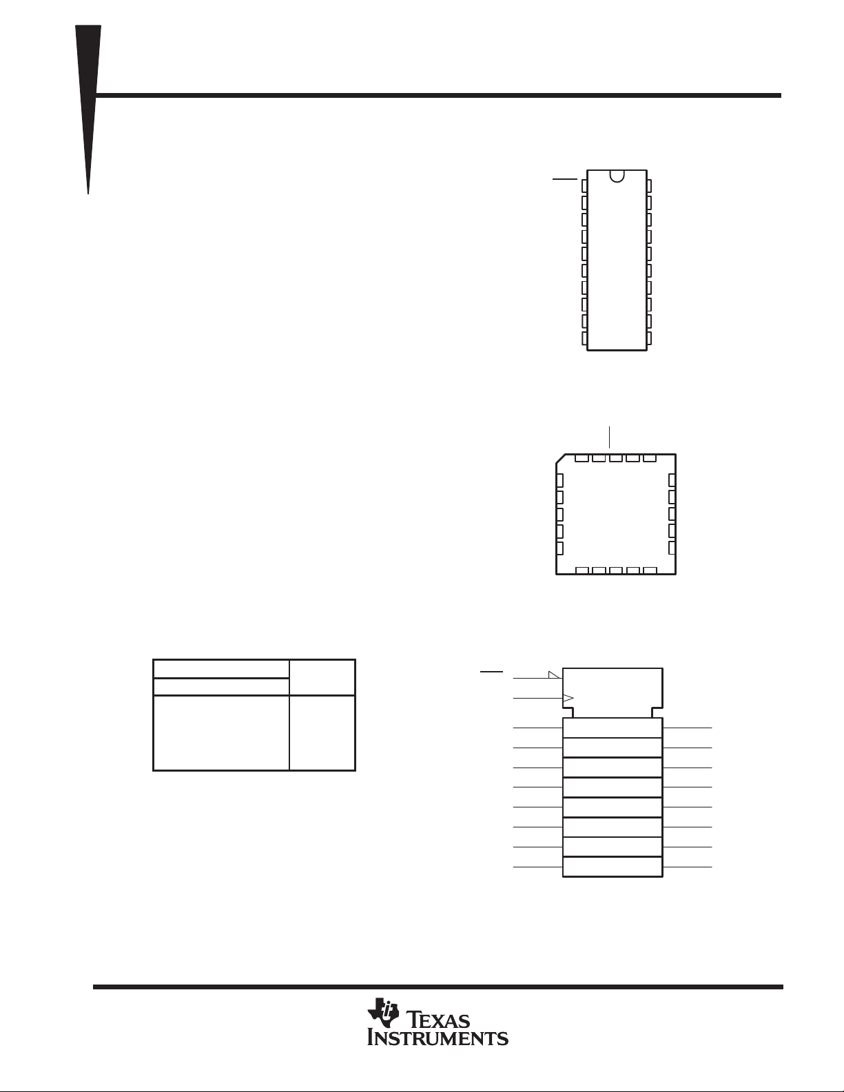
SN54273, SN74LS273 ...J OR W PACKAGE
SN74273 ...N PACKAGE
SN74LS273 . . . DW OR N PACKAGE
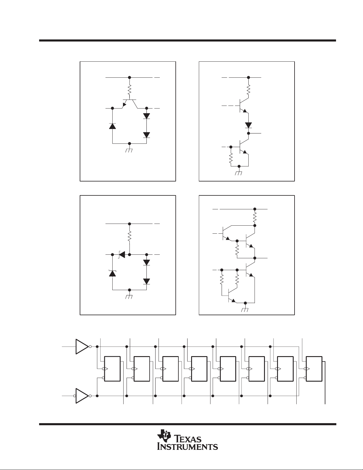
SN54LS273 . . . FK PACKAGE
CLR
1Q
1D
2D
2Q
3Q
3D
4D
4Q
GND
(TOP VIEW)
1
20
2
19
3
18
4
17
5
16
6
15
7
14
8
13
9
12
10
11
(TOP VIEW)
V
CC
8Q
8D
7D
7Q
6Q
6D
5D
5Q
CLK
CC
GND
CLK
V
5Q
18
17
16
15
14
8D
7D
7Q
6Q
6D
2D
2Q
3Q
3D
4D
1D1QCLR5D8Q
3212019
4
5
6
7
8
910111213
4Q
FUNCTION TABLE
(each flip-flop)
INPUTS
CLEAR CLOCK D
L X X L
H ↑ HH
H ↑LL
HLXQ
PRODUCTION DATA information is current as of publication date.
Products conform to specifications per the terms of Texas Instruments
standard warranty. Production processing does not necessarily include
testing of all parameters.
OUTPUT
Q
0
1
11
3
4
7
8
13
14
17
18
†
EN
C1
12
15
16
19
2
1Q
5
2Q
6
3Q
9
4Q
5Q
6Q
7Q
8Q
1D
Copyright 1988, Texas Instruments Incorporated
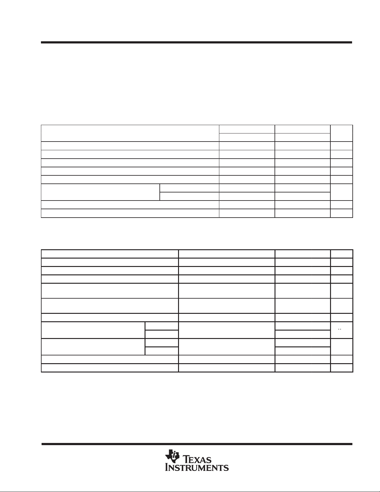
logic symbol
CLR
CLK
1D
2D
3D
4D
5D
6D
7D
8D
†
This symbol is in accordance with ANSI/IEEE Std.
91-1984 and IEC Publication 617-12.
Pin numbers shown are for the DW, J, N, and W packages.
POST OFFICE BOX 655303 • DALLAS, TEXAS 75265
1
Page 2
SN54273, SN54LS273, SN74273, SN74LS273
OCTAL D-TYPE FLIP-FLOP WITH CLEAR
SDLS090 – OCTOBER 1976 – REVISED MARCH 1988
schematics of inputs and outputs
′273
EQUIVALENT OF EACH INPUT
V
CC
R
eq
INPUT
Clear: Req = 3 kΩ NOM
All other inputs: Req = 8 kΩ NOM
EQUIVALENT OF EACH INPUT
V
Clock: Req = 6 kΩ NOM
CC
20 kΩ
NOM
′LS273
TYPICAL OF ALL OUTPUTS
V
CC
100 Ω
NOM
OUTPUT
TYPICAL OF ALL OUTPUTS
V
CC
120 Ω NOM
INPUT
logic diagram (positive logic)
1D
CLOCK
CLEAR
Pin numbers shown are for the DW, J, N, and W packages.
11
1
34
1D
C1
R
1Q
2D
1D
R
2
3D
C1
5
2Q
4D
7
1D
C1
R
6
3Q
5D
8
1D
C1
R
91312
4Q
1D
R
C1
5Q
6D
14
1D
R
C1
OUTPUT
7D
17
15
6Q
1D
R
C1
7Q
16
8D
18
1D
C1
R
19
8Q
2
POST OFFICE BOX 655303 • DALLAS, TEXAS 75265
Page 3
SN54273, SN54LS273, SN74273, SN74LS273
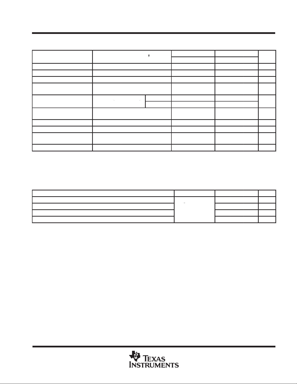
UNIT
Setup time, t
ns
IIHHigh-level input current
V
MAX
V
V
A
IILLow-level input current
V
MAX
V
V
mA
OCTAL D-TYPE FLIP-FLOP WITH CLEAR
SDLS090 – OCTOBER 1976 – REVISED MARCH 1988
absolute maximum ratings over operating free-air temperature range (unless otherwise noted)
Supply voltage, V
(see Note 1) 7 V. . . . . . . . . . . . . . . . . . . . . . . . . . . . . . . . . . . . . . . . . . . . . . . . . . . . . . . . . . . .
CC
Input voltage 5.5 V. . . . . . . . . . . . . . . . . . . . . . . . . . . . . . . . . . . . . . . . . . . . . . . . . . . . . . . . . . . . . . . . . . . . . . . . . . .
Operating free-air temperature range, T
: SN54273 –55°C to 125°C. . . . . . . . . . . . . . . . . . . . . . . . . . . . . . . . .
A
SN74273 0°C to 70°C. . . . . . . . . . . . . . . . . . . . . . . . . . . . . . . . . . . .
Storage temperature range –65°C to 150°C. . . . . . . . . . . . . . . . . . . . . . . . . . . . . . . . . . . . . . . . . . . . . . . . . . . . . . .
NOTE 1: Voltage values are with respect to network ground terminal.
recommended operating conditions
SN54273 SN74273
MIN NOM MAX MIN NOM MAX
Supply voltage, V
High-level output current, I
Low-level output current, I
Clock frequency, f
Width of clock or clear pulse, t
p
Data hold time, t
Operating free-air temperature, T
↑The arrow indicates that the rising edge of the clock pulse is used for reference.
su
CC
OH
OL
clock
w
Data input 20↑ 20↑
Clear inactive state 25↑ 25↑
h
A
4.5 5 5.5 4.75 5 5.25 V
–800 –800 µA
16 16 mA
0 30 0 30 MHz
16.5 16.5 ns
5↑ 5↑ ns
–55 125 0 70 °C
electrical characteristics over recommended operating free-air temperature range (unless
otherwise noted)
PARAMETER TEST CONDITIONS
V
High-level input voltage 2 V
IH
V
Low-level input voltage 0.8 V
IL
V
Input clamp voltage VCC = MIN, II = –12 mA –1.5 V
IK
V
High-level output voltage
OH
V
Low-level output voltage
OL
I
Input current at maximum input voltage VCC = MAX, VI = 5.5 V 1 mA
I
p
p
I
Short-circuit output current
OS
I
Supply current VCC = MAX, See Note 2 62 94 mA
CC
†
For conditions shown as MIN or MAX, use the appropriate value specified under recommended operating conditions.
‡
All typical values are at VCC = 5 V, TA = 25°C.
§
Not more than one output should be shorted at a time.
NOTE 2: With all outputs open and 4.5 V applied to all data and clear inputs, ICC is measured after a momentary ground, then 4.5 V , is applied
to clock.
§
Clear
Clock or D
Clear
Clock or D
VCC = MIN,
VIL = 0.8 V,
VCC = MIN,
VIL = 0.8 V,
=
=
,
,
CC
CC
VCC = MAX –18 –57 mA
†
VIH = 2 V,
IOH = –800 µA
VIH = 2 V,
IOH = 16 mA
= 2.4
I
= 0.4
I
MIN TYP‡MAX UNIT
2.4 3.4 V
0.4 V
80
µ
40
–3.2
–1.6
POST OFFICE BOX 655303 • DALLAS, TEXAS 75265
3
Page 4
SN54273, SN54LS273, SN74273, SN74LS273
R
400 Ω
See Note 3
UNIT
Setup time, t
ns
OCTAL D-TYPE FLIP-FLOP WITH CLEAR
SDLS090 – OCTOBER 1976 – REVISED MARCH 1988
switching characteristics, VCC = 5 V, TA = 25°C
PARAMETER TEST CONDITIONS MIN TYP MAX UNIT
f
Maximum clock frequency
max
t
Propagation delay time, high-to-low-level output from clear
PHL
t
Propagation delay time, low-to-high-level output from clock
PLH
t
Propagation delay time, high-to-low-level output from clock
PHL
NOTE 3: Load circuits and voltage waveforms are shown in Section 1.
CL = 15 pF,
=
L
See Note 3
,
absolute maximum ratings over operating free-air temperature range (unless otherwise noted)
30 40 MHz
18 27 ns
17 27 ns
18 27 ns
Supply voltage, V
(see Note 1) 7 V. . . . . . . . . . . . . . . . . . . . . . . . . . . . . . . . . . . . . . . . . . . . . . . . . . . . . . . . . . . .
CC
Input voltage 7 V. . . . . . . . . . . . . . . . . . . . . . . . . . . . . . . . . . . . . . . . . . . . . . . . . . . . . . . . . . . . . . . . . . . . . . . . . . . . .
Operating free-air temperature range, T
: SN54LS273 –55°C to 125°C. . . . . . . . . . . . . . . . . . . . . . . . . . . . . .
A
SN74LS273 0°C to 70°C. . . . . . . . . . . . . . . . . . . . . . . . . . . . . . . . .
Storage temperature range –65°C to 150°C. . . . . . . . . . . . . . . . . . . . . . . . . . . . . . . . . . . . . . . . . . . . . . . . . . . . . . .
NOTE 1: Voltage values are with respect to network ground terminal.
recommended operating conditions
SN54LS273 SN74LS273
MIN NOM MAX MIN NOM MAX
Supply voltage, V
High-level output current, I
Low-level output current, I
Clock frequency, f
Width of clock or clear pulse, t
p
Data hold time, t
Operating free-air temperature, T
↑The arrow indicates that the rising edge of the clock pulse is used for reference.
su
CC
OH
OL
clock
w
Data input 20↑ 20↑
Clear inactive state 25↑ 25↑
h
A
4.5 5 5.5 4.75 5 5.25 V
–400 –400 µA
4 8 mA
0 30 0 30 MHz
20 20 ns
5↑ 5↑ ns
–55 125 0 70 °C
4
POST OFFICE BOX 655303 • DALLAS, TEXAS 75265
Page 5
SN54273, SN54LS273, SN74273, SN74LS273
PARAMETER
TEST CONDITIONS
†
UNIT
VOLLow-level output voltage
CC
,
IH
,
V
R
See Note 3
OCTAL D-TYPE FLIP-FLOP WITH CLEAR
SDLS090 – OCTOBER 1976 – REVISED MARCH 1988
electrical characteristics over recommended operating free-air temperature range (unless
otherwise noted)
SN54LS273 SN74LS273
MIN TYP‡MAX MIN TYP‡MAX
V
High-level input voltage 2 2 V
IH
V
Low-level input voltage 0.7 0.8 V
IL
V
Input clamp voltage VCC = MIN, II = –18 mA –1.5 –1.5 V
IK
V
High-level output voltage
OH
p
Input current at
I
I
maximum input voltage
I
High-level input current VCC = MAX, VI = 2.7 V 20 20 µA
IH
I
Low-level input current VCC = MAX, VI = 0.4 V –0.4 –0.4 mA
IL
Short-circuit output
I
OS
I
CC
†
For conditions shown as MIN or MAX, use the appropriate value specified under recommended operating conditions.
‡
All typical values are at VCC = 5 V, TA = 25°C.
§
Not more than one output should be shorted at a time and duration of short circuit should not exceed one second.
NOTE 2: With all outputs open and 4.5 V applied to all data and clear inputs, ICC is measured after a momentary ground, then 4.5 V , is applied
§
current
Supply current VCC = MAX, See Note 2 17 27 17 27 mA
to clock.
VCC = MIN,
VIL = VILmax,
V
= MIN, V
VIL = VILmax,
VCC = MAX, VI = 7 V 0.1 0.1 mA
VCC = MAX –20 –100 –20 –100 mA
VIH = 2 V,
IOH = –400 µA
= 2 V,
2.5 3.4 2.7 3.4 V
IOL = 4 mA 0.25 0.4 0.25 0.4
IOL = 8 mA 0.35 0.5
switching characteristics, VCC = 5 V, TA = 25°C
PARAMETER TEST CONDITIONS MIN TYP MAX UNIT
f
Maximum clock frequency
max
t
Propagation delay time, high-to-low-level output from clear
PHL
t
Propagation delay time, low-to-high-level output from clock
PLH
t
Propagation delay time, high-to-low-level output from clock
PHL
NOTE 3: Load circuits and voltage waveforms are shown in Section 1.
CL = 15 pF,
= 2 kΩ,
L
See Note 3
30 40 MHz
18 27 ns
17 27 ns
18 27 ns
POST OFFICE BOX 655303 • DALLAS, TEXAS 75265
5
Page 6

IMPORTANT NOTICE
T exas Instruments and its subsidiaries (TI) reserve the right to make changes to their products or to discontinue
any product or service without notice, and advise customers to obtain the latest version of relevant information
to verify, before placing orders, that information being relied on is current and complete. All products are sold
subject to the terms and conditions of sale supplied at the time of order acknowledgement, including those
pertaining to warranty, patent infringement, and limitation of liability.
TI warrants performance of its semiconductor products to the specifications applicable at the time of sale in
accordance with TI’s standard warranty. Testing and other quality control techniques are utilized to the extent
TI deems necessary to support this warranty . Specific testing of all parameters of each device is not necessarily
performed, except those mandated by government requirements.
CERT AIN APPLICATIONS USING SEMICONDUCTOR PRODUCTS MAY INVOL VE POTENTIAL RISKS OF
DEATH, PERSONAL INJURY, OR SEVERE PROPERTY OR ENVIRONMENTAL DAMAGE (“CRITICAL
APPLICATIONS”). TI SEMICONDUCTOR PRODUCTS ARE NOT DESIGNED, AUTHORIZED, OR
WARRANTED TO BE SUITABLE FOR USE IN LIFE-SUPPORT DEVICES OR SYSTEMS OR OTHER
CRITICAL APPLICA TIONS. INCLUSION OF TI PRODUCTS IN SUCH APPLICATIONS IS UNDERST OOD TO
BE FULLY AT THE CUSTOMER’S RISK.
In order to minimize risks associated with the customer’s applications, adequate design and operating
safeguards must be provided by the customer to minimize inherent or procedural hazards.
TI assumes no liability for applications assistance or customer product design. TI does not warrant or represent
that any license, either express or implied, is granted under any patent right, copyright, mask work right, or other
intellectual property right of TI covering or relating to any combination, machine, or process in which such
semiconductor products or services might be or are used. TI’s publication of information regarding any third
party’s products or services does not constitute TI’s approval, warranty or endorsement thereof.
Copyright 1998, Texas Instruments Incorporated
 Loading...