

Page 1
7406
SOIC
D
7416
PDIP
N
Tube
CDIP
J
CDIP
W
查询SN7406供应商
SN5406, SN5416, SN7406, SN7416
HEX INVERTER BUFFERS/DRIVERS
WITH OPEN-COLLECTOR HIGH-VOLTAGE OUTPUTS
SDLS031A – DECEMBER 1983 – REVISED DECEMBER 2001
D
Convert TTL Voltage Levels to MOS Levels
D
High Sink-Current Capability
D
Input Clamping Diodes Simplify System
Design
D
Open-Collector Drivers for Indicator Lamps
and Relays
D
Inputs Fully Compatible With Most TTL
Circuits
description
These TTL hex inverter buffers/drivers feature
high-voltage open-collector outputs for interfacing
with high-level circuits (such as MOS) or for
driving high-current loads (such as lamps or
relays), and also are characterized for use as
inverter buffers for driving TTL inputs. The
SN5406 and SN7406 have minimum breakdown
voltages of 30 V . The SN5416 and SN7416 have
minimum breakdown voltages of 15 V. The
maximum sink current is 30 mA for the SN5406
and SN5416, and 40 mA for the SN7406 and
SN7416.
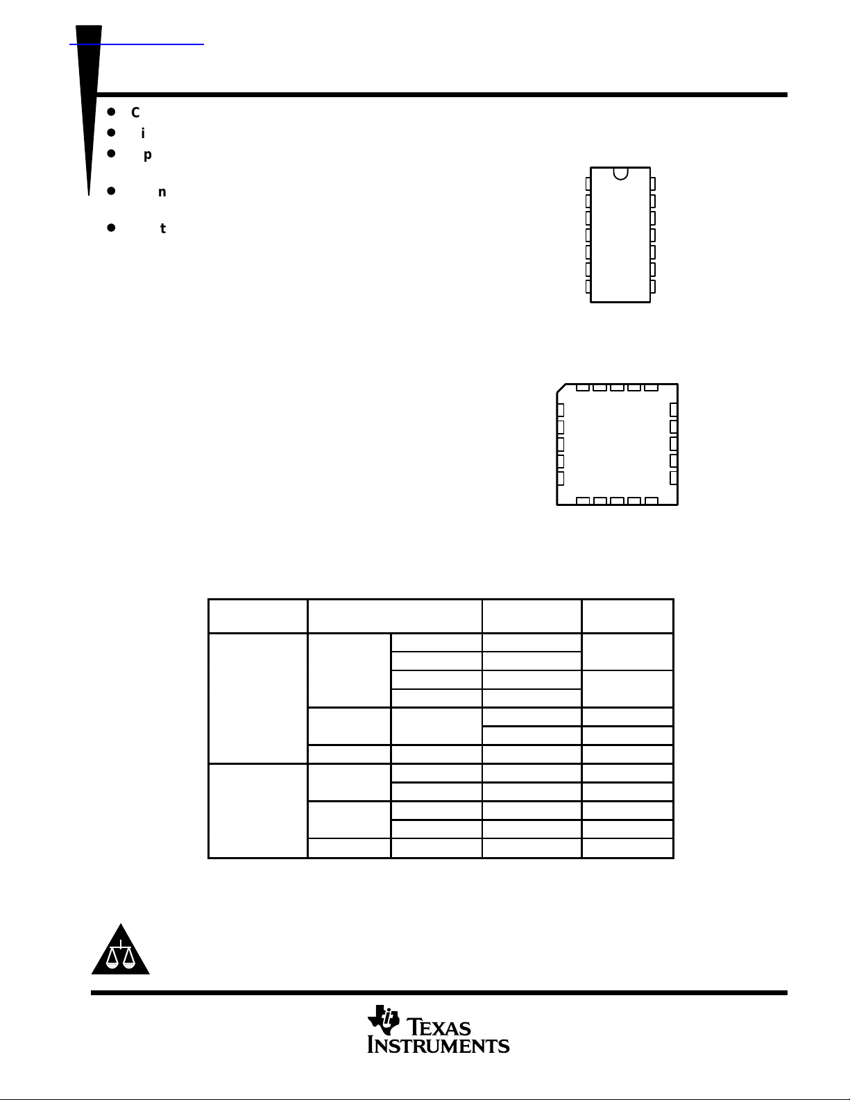
SN5406, SN5416 ...J OR W PACKAGE
SN7406 . . . D, N, OR NS PACKAGE
SN7416 ...D OR N PACKAGE
2A
NC
2Y
NC
3A
(TOP VIEW)
1A
1
1Y
2
2A
3
2Y
4
3A
5
3Y
6
GND
SN5406 . . . FK PACKAGE
7
(TOP VIEW)
1Y1ANC6A6A
3212019
4
5
6
7
8
910111213
14
13
12
11
10
V
9
8
CC
18
17
16
15
14
V
6A
6Y
5A
5Y
4A
4Y
CC
6Y
NC
5A
NC
5Y
GND
NC
4Y
3Y
NC – No internal connection
ORDERING INFORMATION
T
A
0°C to 70°C
SOP – NS Tape and reel SN7406NSR SN7406
–55°C to 125°C
LCCC – FK Tube SNJ5406FK SNJ5406FK
†
Package drawings, standard packing quantities, thermal data, symbolization, and PCB design
guidelines are available at www.ti.com/sc/package.
PACKAGE
–
–
–
–
†
Tube SN7406D
Tape and reel SN7406DR
Tube SN7416D
Tape and reel SN7416DR
Tube SNJ5406J SNJ5406J
Tube SNJ5416J SNJ5416J
Tube SNJ5406W SNJ5406W
Tube SNJ5416W SNJ5416W
ORDERABLE
PART NUMBER
SN7406N SN7406N
SN7416N SN7416N
TOP-SIDE
MARKING
Please be aware that an important notice concerning availability, standard warranty, and use in critical applications of
Texas Instruments semiconductor products and disclaimers thereto appears at the end of this data sheet.
PRODUCTION DATA information is current as of publication date.
Products conform to specifications per the terms of Texas Instruments
standard warranty. Production processing does not necessarily include
testing of all parameters.
POST OFFICE BOX 655303 • DALLAS, TEXAS 75265
Copyright 2001, Texas Instruments Incorporated
On products compliant to MIL-PRF-38535, all parameters are tested
unless otherwise noted. On all other products, production
processing does not necessarily include testing of all parameters.
1
Page 2
SN5406, SN5416, SN7406, SN7416
HEX INVERTER BUFFERS/DRIVERS
WITH OPEN-COLLECTOR HIGH-VOLTAGE OUTPUTS
SDLS031A – DECEMBER 1983 – REVISED DECEMBER 2001
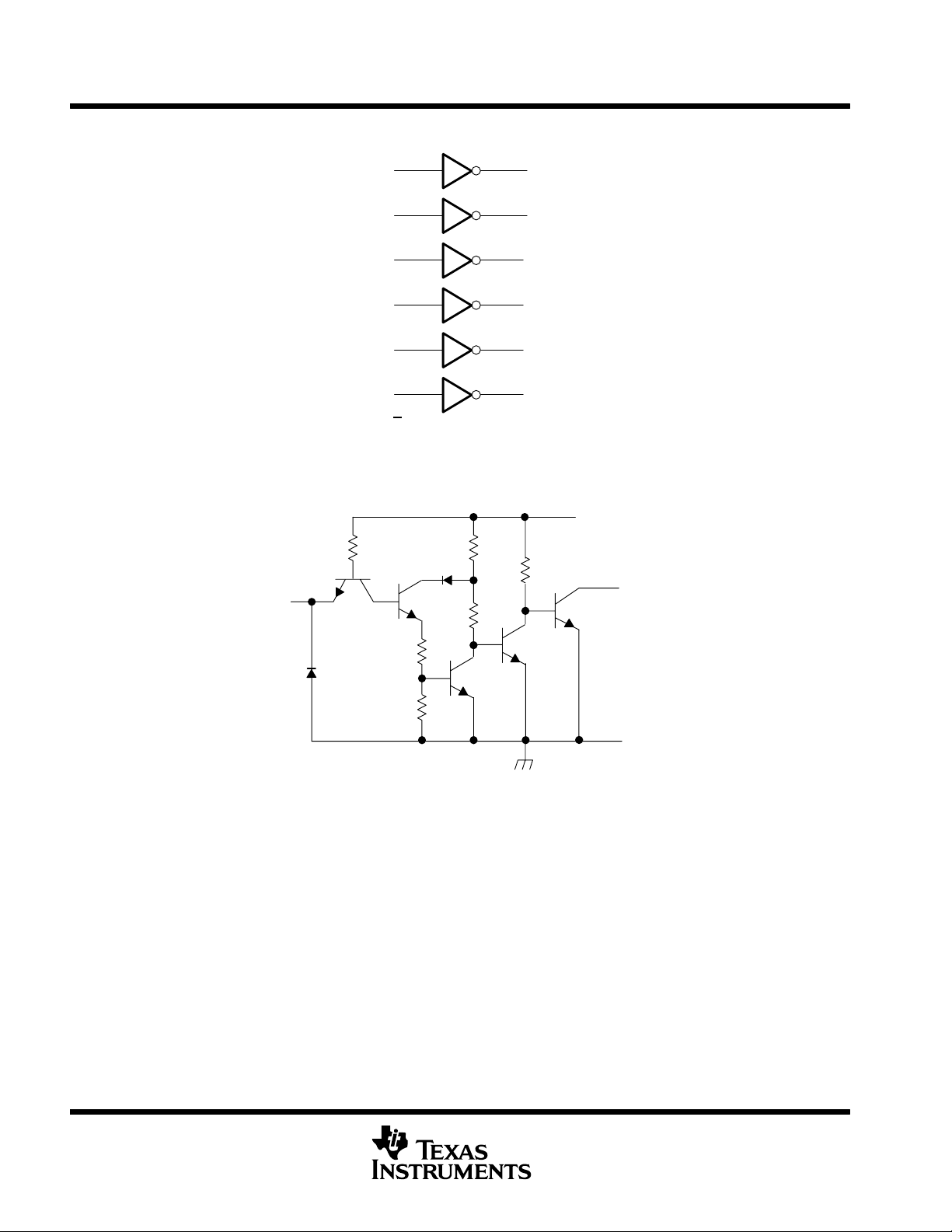
logic diagram (positive logic)
schematic (each buffer/driver)
Input A
6 kΩ
1A
2A
3A
4A
5A
6A
Y = A
1
3
5
9
11
13
1.4 kΩ
2 kΩ
10
12
’06, ’16
2
4
6
8
1Y
2Y
3Y
4Y
5Y
6Y
1.6 kΩ
V
CC
Output Y
100 Ω
1 kΩ
GND
Resistor values shown are nominal.
absolute maximum ratings over operating free-air temperature (unless otherwise noted)
Supply voltage, V
Input voltage, V
Output voltage, V
(see Note 1) 7 V. . . . . . . . . . . . . . . . . . . . . . . . . . . . . . . . . . . . . . . . . . . . . . . . . . . . . . . . . . . . .
CC
(see Note 1) 5.5 V. . . . . . . . . . . . . . . . . . . . . . . . . . . . . . . . . . . . . . . . . . . . . . . . . . . . . . . . . . . . . . .
I
(see Notes 1 and 2): SN5406, SN7406 30 V. . . . . . . . . . . . . . . . . . . . . . . . . . . . . . . . . . . . . .
O
†
SN5416, SN7416 15 V. . . . . . . . . . . . . . . . . . . . . . . . . . . . . . . . . . . . . .
Package thermal impedance, θ
(see Note 3): D package 86°C/W. . . . . . . . . . . . . . . . . . . . . . . . . . . . . . . . . . .
JA
N package 80°C/W. . . . . . . . . . . . . . . . . . . . . . . . . . . . . . . . . . .
NS package 76°C/W. . . . . . . . . . . . . . . . . . . . . . . . . . . . . . . . .
Storage temperature range, T
†
Stresses beyond those listed under “absolute maximum ratings” may cause permanent damage to the device. These are stress ratings only, and
functional operation of the device at these or any other conditions beyond those indicated under “recommended operating conditions” is not
implied. Exposure to absolute-maximum-rated conditions for extended periods may affect device reliability.
NOTES: 1. Voltage values are with respect to network ground terminal.
2. This is the maximum voltage which should be applied to any output when it is in the off state.
3. The package thermal impedance is calculated in accordance with JESD 51-7.
–65°C to 150°C. . . . . . . . . . . . . . . . . . . . . . . . . . . . . . . . . . . . . . . . . . . . . . . . . . .
stg
2
POST OFFICE BOX 655303 • DALLAS, TEXAS 75265
Page 3
VOHHigh-level output voltage
V
†
VOLV
MIN
V
2 V
V
A
Y
R
110 Ω
C
15 pF
ns
SN5406, SN5416, SN7406, SN7416
HEX INVERTER BUFFERS/DRIVERS
WITH OPEN-COLLECTOR HIGH-VOLTAGE OUTPUTS
SDLS031A – DECEMBER 1983 – REVISED DECEMBER 2001
recommended operating conditions
SN5406
SN5416
MIN NOM MAX MIN NOM MAX
V
Supply voltage 4.5 5 5.5 4.75 5 5.25 V
CC
V
High-level input voltage 2 2 V
IH
V
Low-level input voltage 0.8 0.8 V
IL
p
I
Low-level output current 30 40 mA
OL
T
Operating free-air temperature –55 125 0 70 °C
A
’06 30 30
’16 15 15
electrical characteristics over recommended operating free-air temperature range (unless
otherwise noted)
SN5406
PARAMETER
V
IK
I
OH
I
I
I
IH
I
IL
I
CCH
I
CCL
†
For conditions shown as MIN or MAX, use the appropriate value specified under recommended operating conditions.
‡
All typical values are at VCC = 5 V, TA = 25°C.
§
VOH = 30 V for ’06 and 15 V for ’16.
¶
IOL = 30 mA for SN54’ and 40 mA for SN74’.
VCC = MIN, II = –12 mA –1.5 –1.5 V
VCC = MIN, VIL = 0.8 V, VOH = § 0.25 0.25 mA
=
CC
VCC = MAX, VI = 5.5 V 1 1 mA
VCC = MAX, VIH = 2.4 V 40 40 µA
VCC = MAX, VIL = 0.4 V –1.6 –1.6 mA
VCC = MAX 30 48 30 48 mA
VCC = MAX 32 51 32 51 mA
TEST CONDITIONS
,
=
IH
IOL = 16 mA 0.4 0.4
IOL = ¶ 0.7 0.7
SN5416
MIN TYP‡MAX MIN TYP‡MAX
SN7406
SN7416
SN7406
SN7416
UNIT
UNIT
switching characteristics, VCC = 5 V, TA = 25°C (see Figure 1)
PARAMETER
t
PLH
t
PHL
FROM
(INPUT)
POST OFFICE BOX 655303 • DALLAS, TEXAS 75265
TO
(OUTPUT)
TEST CONDITIONS MIN TYP MAX UNIT
,
=
L
=
L
10 15
15 23
3
Page 4

SN5406, SN5416, SN7406, SN7416
HEX INVERTER BUFFERS/DRIVERS
WITH OPEN-COLLECTOR HIGH-VOLTAGE OUTPUTS
SDLS031A – DECEMBER 1983 – REVISED DECEMBER 2001
PARAMETER MEASUREMENT INFORMATION
V
CC
R
L
From Output
Under Test
C
L
(see Note A)
LOAD CIRCUIT
Input
High-Level
Pulse
Low-Level
Pulse
1.5 V 1.5 V
t
w
1.5 V 1.5 V
VOLTAGE WAVEFORMS
PULSE WIDTHS
In-Phase
Output
Out-of-Phase
Output
Test Point
1.5 V 1.5 V
t
PLH
1.5 V 1.5 V
t
PHL
1.5 V 1.5 V
VOLTAGE WAVEFORMS
PROPAGATION DELAY TIMES
t
PHL
t
PLH
3 V
0 V
V
V
V
V
OH
OL
OH
OL
NOTES: A. CL includes probe and jig capacitance.
B. In the examples above, the phase relationships between inputs and outputs have been chosen arbitrarily.
C. All input pulses are supplied by generators having the following characteristics: PRR ≤ 1 MHz, ZO = 50 Ω, tr ≤ 7 ns, tf≤ 7 ns.
D. The outputs are measured one at a time with one input transition per measurement.
Figure 1. Load Circuit and Voltage Waveforms
4
POST OFFICE BOX 655303 • DALLAS, TEXAS 75265
Page 5

PACKAGE OPTION ADDENDUM
www.ti.com
28-Feb-2005
PACKAGING INFORMATION
Orderable Device Status
(1)
Package
Type
Package
Drawing
Pins Package
Qty
Eco Plan
JM38510/00801BCA ACTIVE CDIP J 14 1 None Call TI Level-NC-NC-NC
JM38510/00801BDA ACTIVE CFP W 14 1 None Call TI Level-NC-NC-NC
SN5406J ACTIVE CDIP J 14 1 None Call TI Level-NC-NC-NC
SN5416J ACTIVE CDIP J 14 1 None Call TI Level-NC-NC-NC
SN7406D ACTIVE SOIC D 14 50 Pb-Free
SN7406DR ACTIVE SOIC D 14 2500 Pb-Free
SN7406J OBSOLETE CDIP J 14 None Call TI Call TI
SN7406N ACTIVE PDIP N 14 25 Pb-Free
SN7406N3 OBSOLETE PDIP N 14 None Call TI Call TI
SN7406NSR ACTIVE SO NS 14 2000 Pb-Free
SN7416D ACTIVE SOIC D 14 50 Pb-Free
SN7416DR ACTIVE SOIC D 14 2500 Pb-Free
SN7416N ACTIVE PDIP N 14 25 Pb-Free
SN7416N3 OBSOLETE PDIP N 14 None Call TI Call TI
SN7416NSR ACTIVE SO NS 14 2000 Pb-Free
SNJ5406FK ACTIVE LCCC FK 20 1 None Call TI Level-NC-NC-NC
SNJ5406J ACTIVE CDIP J 14 1 None Call TI Level-NC-NC-NC
SNJ5406W ACTIVE CFP W 14 1 None Call TI Level-NC-NC-NC
SNJ5416J ACTIVE CDIP J 14 1 None Call TI Level-NC-NC-NC
SNJ5416W ACTIVE CFP W 14 1 None Call TI Level-NC-NC-NC
(1)
The marketing status values are defined as follows:
ACTIVE: Product device recommended for new designs.
LIFEBUY: TI has announced that the device willbe discontinued, and a lifetime-buy period is in effect.
NRND: Not recommended for new designs. Device is in production to support existing customers, but TI does not recommend using this part in
a new design.
PREVIEW: Device has been announced but is not in production. Samples may or may not be available.
OBSOLETE: TI has discontinued the production of the device.
(RoHS)
(RoHS)
(RoHS)
(RoHS)
(RoHS)
(RoHS)
(RoHS)
(RoHS)
(2)
Lead/Ball Finish MSL Peak Temp
CU NIPDAU Level-2-260C-1 YEAR/
Level-1-235C-UNLIM
CU NIPDAU Level-2-260C-1 YEAR/
Level-1-235C-UNLIM
CU NIPDAU Level-NC-NC-NC
CU NIPDAU Level-2-260C-1 YEAR/
Level-1-235C-UNLIM
CU NIPDAU Level-2-260C-1 YEAR/
Level-1-235C-UNLIM
CU NIPDAU Level-2-260C-1 YEAR/
Level-1-235C-UNLIM
CU NIPDAU Level-NC-NC-NC
CU NIPDAU Level-2-260C-1 YEAR/
Level-1-235C-UNLIM
(3)
(2)
Eco Plan - May not be currently available - please check http://www.ti.com/productcontent for the latest availability information and additional
product content details.
None: Not yet available Lead (Pb-Free).
Pb-Free (RoHS): TI's terms "Lead-Free" or "Pb-Free" mean semiconductor products that are compatible with the current RoHS requirements
for all 6 substances, including the requirement that lead not exceed 0.1% by weight in homogeneous materials. Where designed to be soldered
at high temperatures, TI Pb-Free products are suitable for use in specified lead-free processes.
Green (RoHS & no Sb/Br): TI defines "Green" to mean "Pb-Free" and in addition, uses package materials that do not contain halogens,
including bromine (Br) or antimony (Sb) above 0.1% of total product weight.
(3)
MSL, Peak Temp. -- The Moisture Sensitivity Level rating according to the JEDECindustry standard classifications, and peak solder
temperature.
Important Information and Disclaimer:The information provided on this page represents TI's knowledge and belief as of the date that it is
Addendum-Page 1
Page 6

PACKAGE OPTION ADDENDUM
www.ti.com
provided. TI bases its knowledge and belief on information provided by third parties, and makes no representation or warranty as to the
accuracy of such information. Efforts are underway to better integrate information from third parties. TI has taken and continues to take
reasonable steps to provide representative and accurate information but may not have conducted destructive testing or chemical analysis on
incoming materials and chemicals. TI and TI suppliers consider certain information to be proprietary, and thus CAS numbers and other limited
information may not be available for release.
In no event shall TI's liability arising out of such information exceed the total purchase price of the TI part(s) at issue in this document sold by TI
to Customer on an annual basis.
28-Feb-2005
Addendum-Page 2
Page 7

IMPORTANT NOTICE
Texas Instruments Incorporated and its subsidiaries (TI) reserve the right to make corrections, modifications,
enhancements, improvements, and other changes to its products and services at any time and to discontinue
any product or service without notice. Customers should obtain the latest relevant information before placing
orders and should verify that such information is current and complete. All products are sold subject to TI’s terms
and conditions of sale supplied at the time of order acknowledgment.
TI warrants performance of its hardware products to the specifications applicable at the time of sale in
accordance with TI’s standard warranty. Testing and other quality control techniques are used to the extent TI
deems necessary to support this warranty . Except where mandated by government requirements, testing of all
parameters of each product is not necessarily performed.
TI assumes no liability for applications assistance or customer product design. Customers are responsible for
their products and applications using TI components. To minimize the risks associated with customer products
and applications, customers should provide adequate design and operating safeguards.
TI does not warrant or represent that any license, either express or implied, is granted under any TI patent right,
copyright, mask work right, or other TI intellectual property right relating to any combination, machine, or process
in which TI products or services are used. Information published by TI regarding third-party products or services
does not constitute a license from TI to use such products or services or a warranty or endorsement thereof.
Use of such information may require a license from a third party under the patents or other intellectual property
of the third party, or a license from TI under the patents or other intellectual property of TI.
Reproduction of information in TI data books or data sheets is permissible only if reproduction is without
alteration and is accompanied by all associated warranties, conditions, limitations, and notices. Reproduction
of this information with alteration is an unfair and deceptive business practice. TI is not responsible or liable for
such altered documentation.
Resale of TI products or services with statements different from or beyond the parameters stated by TI for that
product or service voids all express and any implied warranties for the associated TI product or service and
is an unfair and deceptive business practice. TI is not responsible or liable for any such statements.
Following are URLs where you can obtain information on other Texas Instruments products and application
solutions:
Products Applications
Amplifiers amplifier.ti.com Audio www.ti.com/audio
Data Converters dataconverter.ti.com Automotive www.ti.com/automotive
DSP dsp.ti.com Broadband www.ti.com/broadband
Interface interface.ti.com Digital Control www.ti.com/digitalcontrol
Logic logic.ti.com Military www.ti.com/military
Power Mgmt power.ti.com Optical Networking www.ti.com/opticalnetwork
Microcontrollers microcontroller.ti.com Security www.ti.com/security
Telephony www.ti.com/telephony
Video & Imaging www.ti.com/video
Wireless www.ti.com/wireless
Mailing Address: Texas Instruments
Post Office Box 655303 Dallas, Texas 75265
Copyright 2005, Texas Instruments Incorporated
 Loading...