

Page 1
SN28835
1/2-INCH NTSC TIMER
SOCS023B – FEBRUARY 1991
Copyright 1991, Texas Instruments Incorporated
1
POST OFFICE BOX 655303 • DALLAS, TEXAS 75265
• NTSC-Timing Operation
• Solid-State Reliability
• Color and Monochrome Operation
• Four Selectable-Antiblooming Modes
• Variable-Integration-Time Option
• Surface-Mount Package
• Clamp-Pulse Select Option
• Horizontal and Vertical Resets for External
Synchronization
description
The SN28835 is a monolithic integrated circuit
designed to supply timing signals for the Texas
Instruments (TI) 8-mm TC242/TC244 color and
TC243/TC245 monochrome CCD image sensors.
The SN28835 supplies both CCD-drive signals
and NTSC-television synchronization signals at
standard video rates. It requires a single
5-V supply voltage and a 14.318-MHz
crystal-oscillator input. The SN28835 provides the
user with several options including multiple
antiblooming modes, variable-integration time,
external synchronization, and delayed horizontal
transfer.
The SN28835 is designed to drive the CCD image sensor through intermediary level-shifting devices such as
the TI TMS3473B parallel driver and the SN28846 serial driver. It also supplies sample-and-hold signals for the
TI TL1593 3-channel sample-and-hold circuit and multiplex signals for the TI TL1051 video preprocessor. The
SN28835 NTSC synchronization-signal outputs include composite sync, composite blank, clamp, subcarrier,
subcarrier delayed by 90 degrees, and burst flag.
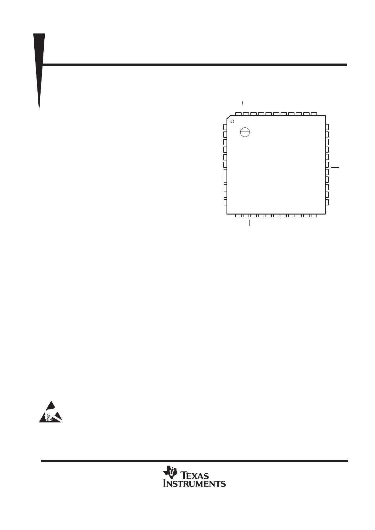
The SN28835 is supplied in a 44-pin plastic flat package and is characterized for operation from –20°C to 45°C.
This device contains circuits to protect its inputs and outputs against damage due to high static voltages or electrostatic fields. These
circuits have been qualified to protect this device against electrostatic discharges (ESD) of up to 2 kV according to MIL-STD-883C,
Method 3015; however, precautions should be taken to avoid application of any voltage higher than maximum-rated voltages to these
high-impedance circuits. During storage or handling, the device leads should be shorted together or the device should be placed in
conductive foam. In a circuit, unused inputs should always be connected to an appropriated logic voltage level, preferably either VCC or ground.
Specific guidelines for handling devices of this type are contained in the publication
Guidelines for Handling Electrostatic-Discharge-Sensitive
(ESDS) Devices and Assemblies
available from Texas Instruments.
TI is a trademark of Texas Instruments Incorporated.
GND
MODE
PI
ABIN
GT
PS
PD
S3
S2
S1
T
12 13
1
2
3
4
5
6
7
8
9
10
11
BCP1
BCP2
CP2
CP1
CSYNC
CBLK
BF
SC
SC(90)
ABS0
ABS1
14 15 16 17
GT3/SH2
SH1X2X1
43 42 41 40 3944 38
FI
E/L
VDS
HCR
VCR
GT2
GT1/SH3
VGATE
HGATE
CLK2M
V
HIGH
GPS
SB
GP
VD
VD2
WHTA
36 35 3437
18 19 20 21 22
CC
FS PACKAGE
(TOP VIEW)
33
32
31
30
29
28
27
26
25
24
23
PRODUCTION DATA information is current as of publication date.
Products conform to specifications per the terms of Texas Instruments
standard warranty. Production processing does not necessarily include
testing of all parameters.
Page 2
SN28835
1/2-INCH NTSC TIMER
SOCS023B – FEBRUARY 1991
2
POST OFFICE BOX 655303 • DALLAS, TEXAS 75265
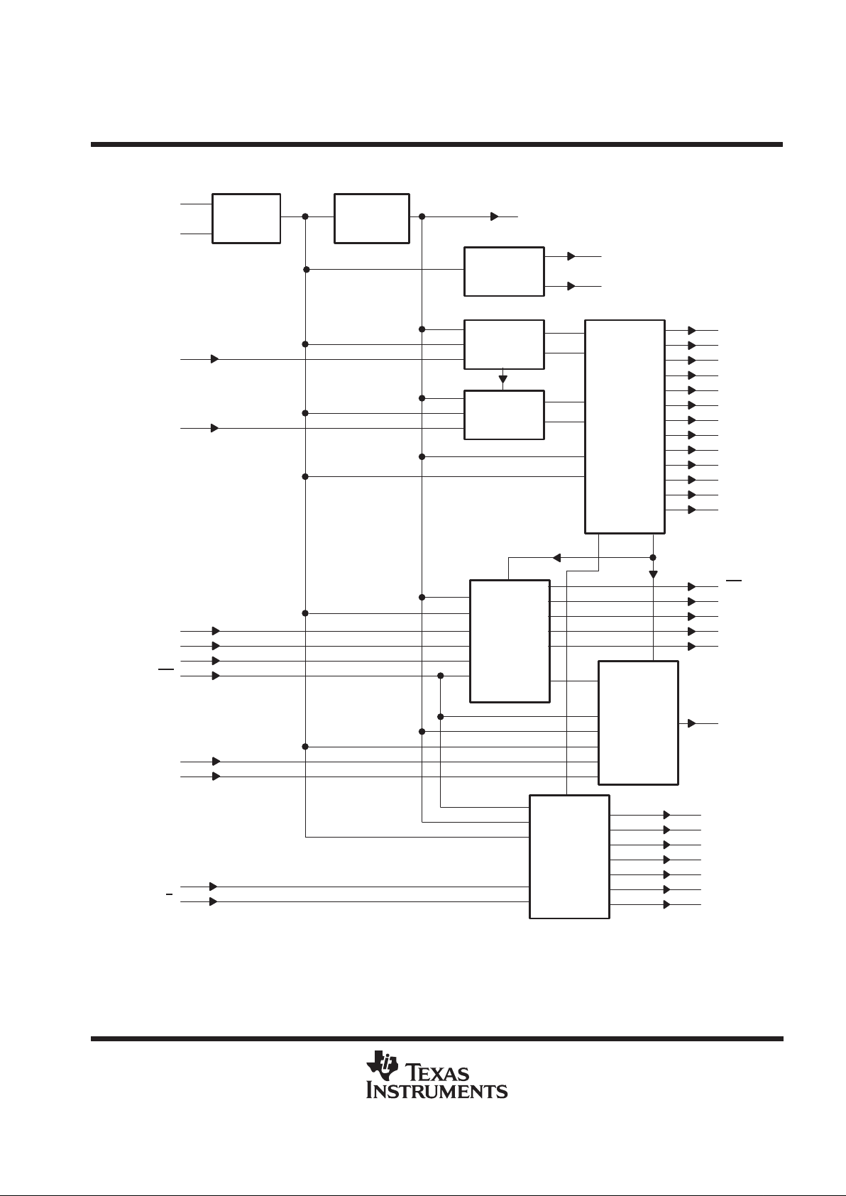
functional block diagram
Oscillator
Divide
by 7
14.318
MHz
2.045 MHz
Divide by 4,
Phase Shift
Horizontal
Counter
Vertical
Counter
Clock
Generator
Antiblooming
Generator
Serial
Generator
Decoder
27
29
31
28
23
1
BCP1
BCP2
CP1
CP2
CSYNC
CBLK
BF
VD
FI
VGATE
HGATE
WHTA
VD2
PD
GT
PI
PS
T
S1
S2
S3
SH1
GT3/SH2
GT1/SH3
GT2
24
25
26
36
37
38
39
30
ABIN
13
15
42
14
GPS
GP
VDS
SB
ABS0
ABS1
10
11
MODE
E/L
32
43
HCR
41
VCR
40
X1
34
X2
35
9
SC(90)
8
SC
21
CLK2M
2
4
3
5
6
7
16
44
19
20
18
17
Page 3
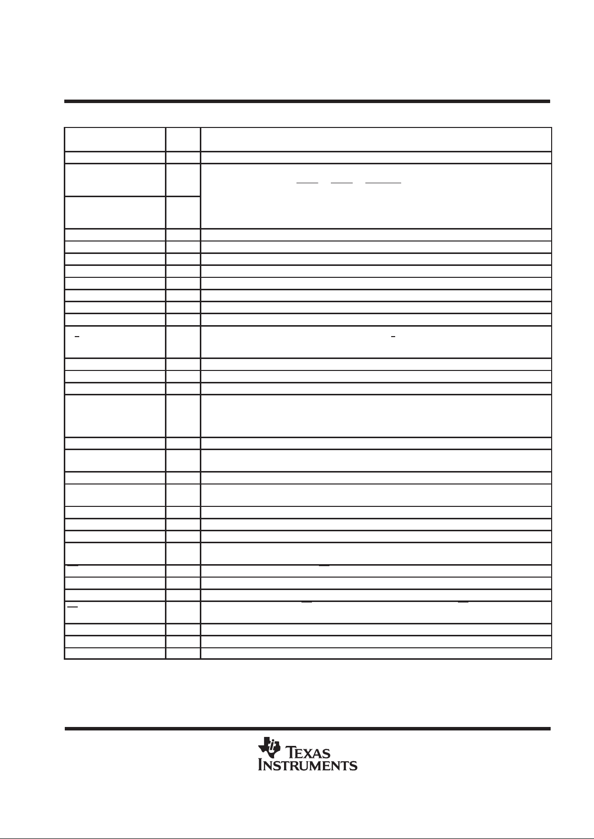
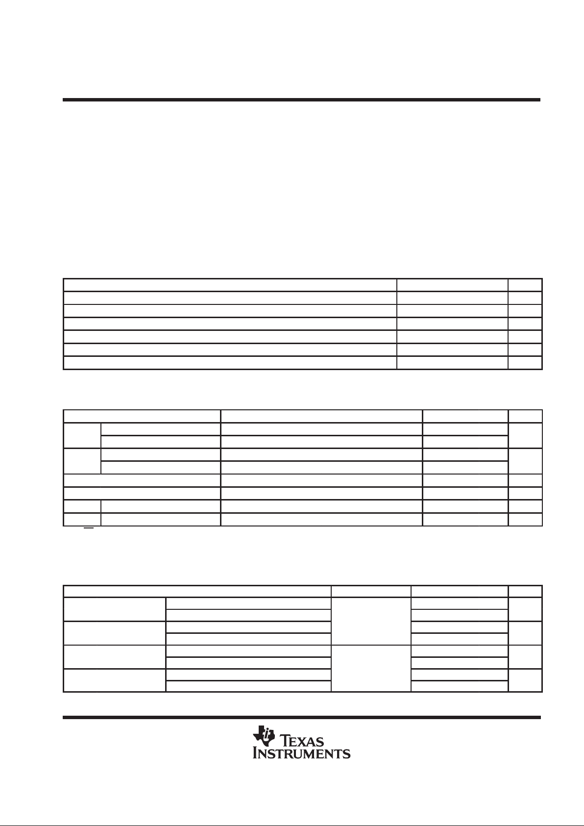
The levels on these two terminals determine which of the four antiblooming modes is selected:
ABS1 ABS0 Operation
L L No ABG pulses
L H 2-MHz burst of ABG pulses
H L 1-MHz burst of ABG pulses
H H 1-MHz continuous ABG pulses
SN28835
1/2-INCH NTSC TIMER
SOCS023B – FEBRUARY 1991
3
POST OFFICE BOX 655303 • DALLAS, TEXAS 75265
Terminal Functions
TERMINAL
NAME NO.
I/O
DESCRIPTION
ABIN 30 O Antiblooming in
ABS0 10 I
ABS1 11 I
BCP1 1 O Optical black clamp
BCP2 2 O Optical black clamp
BF 7 O Burst flag
CBLK 6 O Composite blank
CLK2M 21 O 2-MHz clock
CP1 4 O Clamp
CP2 3 O Clamp
CSYNC 5 O Composite sync
E/L 43 I
Delay select for S1, S2, S3. When E/L is high, the three serial-transfer pulses occur early relative to the
sample-and-hold pulses SH1, SH2, and SH3. When E/L
is low, the three serial-transfer pulses occur
late relative to the sample-and-hold pulses.
FI 44 O Field index
GND 33 Ground
GP 15 I Exposure control: GP gates the PS and PI outputs (see the description of GPS)
GPS 13 I
When GPS is high, the timer operates in the normal-integration-time mode (t
int
= 16.67 ms) and VD is
connected internally to GP . To operate the imager in the variable-integration-time mode, GPS must be
held low and a user-defined logic circuit must be inserted between VD and GP to vary the integration
time (see Figure 1).
GT 29 O TMS3473B parallel-driver MIDSEL input switch
GT1/SH3 38 O
GT1/SH3 is a logic signal for both Y gate 1 of the TL1051 video preprocessor and sample-and-hold
channel 3 of the TL1593 3-channel sample-and-hold circuit.
GT2 39 O Y gate 2 for the TL1051 video preprocessor
GT3/SH2 37 O
GT3/SH2 is a logic signal for both Y gate 3 and sample-and-hold channel 2 of the TL1051 video
preprocessor.
HCR 41 I Horizontal-counter reset
HGATE 20 O Decoded H count signal. HGATE is a test point and is not used in normal operation.
HIGH 12 I Not used (tie high)
MODE 32 I
TC243/TC245 CCD select. When MODE is low, the TC244/245 CCD imager is selected; when MODE
is high, the TC242/243 is selected (see the appropriate data sheets for imager differences).
PD 27 O Power down. A low-logic level on PD causes the device to enter a low power-consumption mode.
PI 31 O Parallel-image-area gate clock
PS 28 O Parallel-storage-area gate clock
SB 14 I
Standby-mode select. When SB is high, normal operation is selected; when SB is low, the power-down
mode is selected.
SC 8 O Subcarrier
SC(90) 9 O Subcarrier phase shifted by 90 degrees
SH1 36 O Sample and hold 1
Page 4
SN28835
1/2-INCH NTSC TIMER
SOCS023B – FEBRUARY 1991
4
POST OFFICE BOX 655303 • DALLAS, TEXAS 75265
Terminal Functions (Continued)
TERMINAL
NAME NO.
I/O
DESCRIPTION
S1 24 O Serial clock 1
S2 25 O Serial clock 2
S3 26 O Serial clock 3
T 23 O Transfer-gate clock
V
CC
22 DC power
VCR 40 I Vertical-counter reset
VD 16 O Vertical drive
VDS 42 I
Vertical-dump speed. When VDS is high, the vertical-dump frequency is 3.58MHz; when VDS is low,
the vertical-dump frequency is 2 MHz.
VD2 17 O Real-display-area signal. VD2 is a test point and is not used in normal operation.
VGATE 19 O Decoded V count signal. VGATE is a test point and is not used in normal operation.
WHTA 18 O WHTA is a test point and is not used in normal operation.
X1 34
X2 35
Crystal oscillator (see Figure 2)
12 3
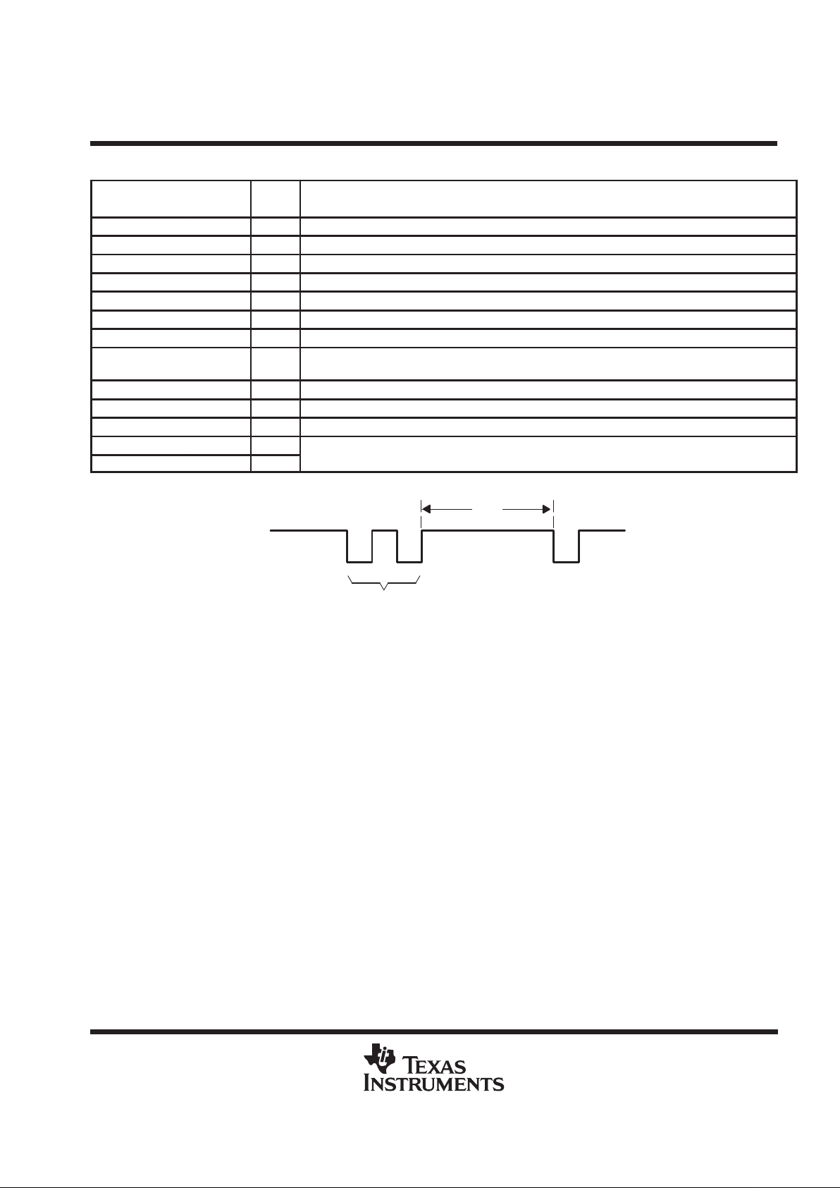
t
int
Flush Pulses Transfer Pulse
GP
Figure 1. GP Flush and Transfer Pulses
Page 5
SN28835
1/2-INCH NTSC TIMER
SOCS023B – FEBRUARY 1991
5
POST OFFICE BOX 655303 • DALLAS, TEXAS 75265
variable-integration-time mode
In addition to the normal TV mode of operation, the SN28835 timing generator offers an optional
variable-integration mode for use with the TC244 and TC245 CCD area-array image sensors. The
variable-integration mode is selected by applying a low-logic level to GPS. This low-logic level disables the
vertical-drive (VD) signal from controlling, internal to the timer, the image-area and storage-area parallel transfer
signal (GP).
Prior to the start of a new integration period, the charge that has accumulated in the image area must be
transferred out. To flush this previous signal or dark-current charge from the image area, GP is pulsed low two
times. Each low pulse generates 256 image-area and storage-area gate and transfer signals that shift the
unwanted charge into the clearing drain. This clearing function should be performed during the high time of the
VD signal (see Figure 3 through Figure 12).
The new integration period continues as long as GP remains high. GPS must be held at a low-logic level to
prevent VD from controlling GP internally . The integration ceases and the readout occurs when VD and GP are
pulsed low simultaneously; this is accomplished by taking GPS to a high-logic level. The readout timing is
dependent on the vertical-drive pulse; this means that the total-integration time is a multiple of 1/60 of a second
plus the time interval between the last GP low pulse and the next VD low pulse. The image readout occurs within
the normal 1/60-second readout interval. If the integration time is less than 1/60 of a second, normal output
operation occurs; if the integration time is greater than 1/60 of a second, a frame buffer may be required to
capture the image.
Integration times greater than 1/60 of a second result in image degradation at temperatures greater than 25°C
due to dark-current generation. The degradation is seen as a decrease in dynamic range (contrast) and an
increase in noise. It is recommended that the image sensor be cooled for long-exposure operation. The
dark-current generation is reduced by a factor of two for each 7°C temperature decrease. The sensor operates
at –30°C. Cooling can be accomplished by using a thermoelectric or Peltier cooler attached to the image sensor .
Condensation on the header must be prevented by isolating the cooled sensor from moist air. V acuum isolation
is preferred; however, the continual flushing of dry nitrogen across the header can also prevent condensation.
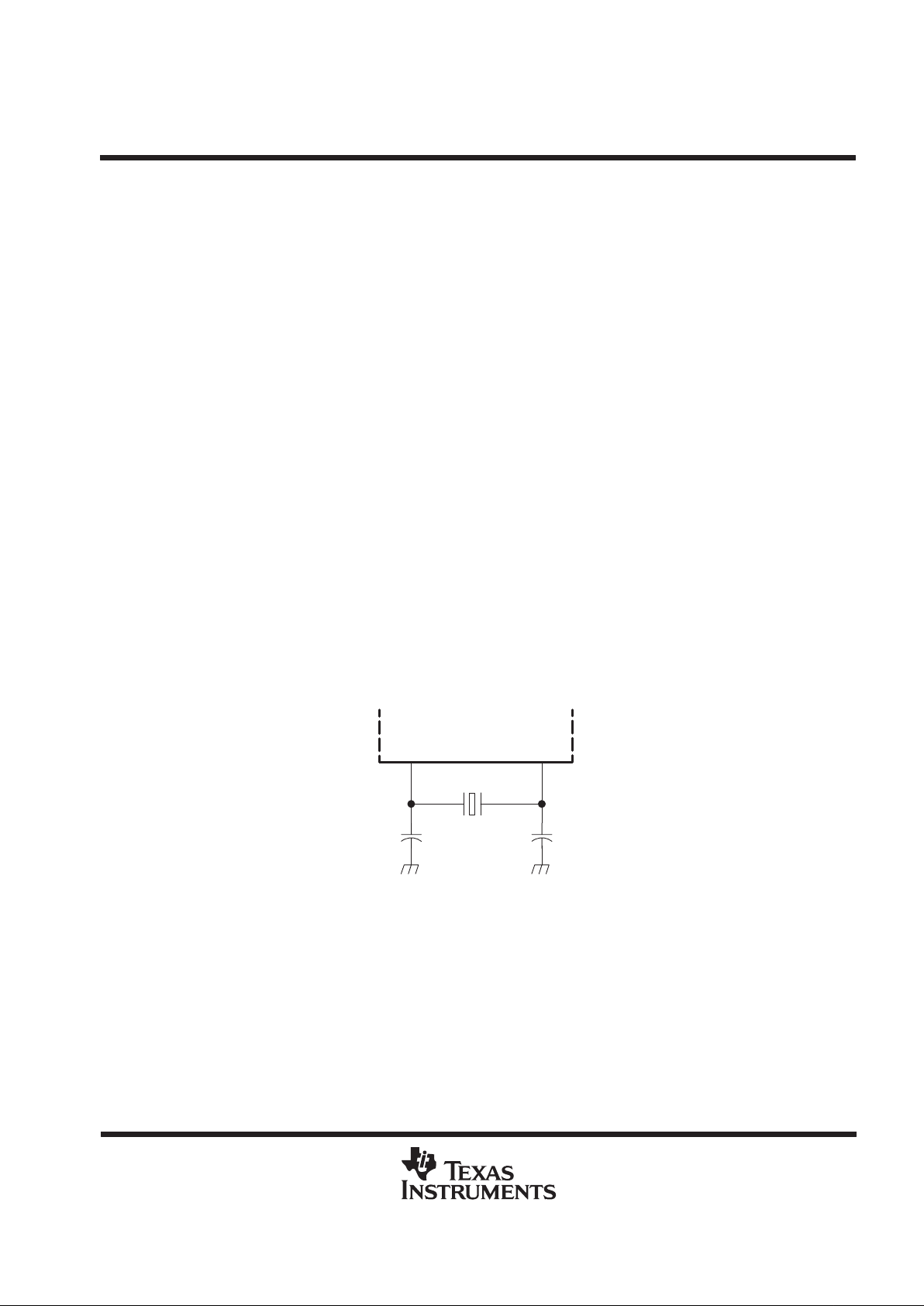
X1 X2
34 35
C1 ≈ 40 pF C2 ≈ 40 pF
SN28835
NOTE: The SN28835 is designed for use with a
crystal oscillator. The X1 and X2
terminals should not connect directly to
external driver outputs.
Figure 2. Connection of an External Crystal Oscillator to the SN28835
Page 6
SN28835
1/2-INCH NTSC TIMER
SOCS023B – FEBRUARY 1991
6
POST OFFICE BOX 655303 • DALLAS, TEXAS 75265
absolute maximum ratings over operating free-air temperature range (unless otherwise noted)
†
Supply voltage range, V
CC
(see Note 1) –0.3 V to 7 V. . . . . . . . . . . . . . . . . . . . . . . . . . . . . . . . . . . . . . . . . . . . . .
Input voltage range, V
I
–0.3 V to VCC + 0.3 V. . . . . . . . . . . . . . . . . . . . . . . . . . . . . . . . . . . . . . . . . . . . . . . . . . . . . .
Output voltage range, V
O
–0.3 V to VCC + 0.3 V. . . . . . . . . . . . . . . . . . . . . . . . . . . . . . . . . . . . . . . . . . . . . . . . . . .
Continuous total power dissipation at (or below) T
A
= 25°C 300 mW. . . . . . . . . . . . . . . . . . . . . . . . . . . . . . . . . .
Operating free-air temperature range, T
A
–20°C to 45°C. . . . . . . . . . . . . . . . . . . . . . . . . . . . . . . . . . . . . . . . . . . .
Storage temperature range, T
STG
–55°C to 125°C. . . . . . . . . . . . . . . . . . . . . . . . . . . . . . . . . . . . . . . . . . . . . . . . .
Lead temperature 1,6 mm (1/16 inch) from case for 10 seconds 260°C. . . . . . . . . . . . . . . . . . . . . . . . . . . . . . .
†
Stresses beyond those listed under “absolute maximum ratings” may cause permanent damage to the device. These are stress ratings only, and
functional operation of the device at these or any other conditions beyond those indicated under “recommended operating conditions” is not
implied. Exposure to absolute-maximum-rated conditions for extended periods may affect device reliability.
NOTE 1: All voltage values are with respect to GND.
recommended operating conditions
MIN NOM MAX UNIT
Supply voltage, V
CC
4.5 5 5.5 V
High-level input voltage, V
IH
VCC x 0.7 V
Low-level input voltage, V
IL 0.8
V
Operating frequency 14.318 MHz
Power-up time 300 µs
Operating free-air temperature, T
A
–20 45 °C
electrical characteristics over recommended ranges of supply voltage and operating free-air
temperature (unless otherwise noted)
‡
PARAMETER TEST CONDITIONS MIN TYP MAX UNIT
GT3/SH2 and GT1/SH3 VCC = 4.5 V, IOH = –4 mA 3.5
V
OH
All other outputs VCC = 4.5 V, IOH = –2 mA 3.5
V
GT3/SH2 and GT1/SH3 VCC = 4.5 V, IOL = 4 mA 0.5
V
OL
All other outputs VCC = 4.5 V, IOL = 2 mA 0.5
V
I
IH
§
VIH = 5 V 1 µA
I
IL
VIL = 0 –30 –200 –500 µA
I
CC(AV)
Average supply current 10 30 mA
I
CC(S)
Standby supply current 1 mA
‡
The SB input is a Schmitt-trigger input with 0.1-V to 1-V hysteresis.
§
All inputs except X1 have pullup-current sources.
switching characteristics over recommended ranges of supply voltage and operating free-air
temperature
PARAMETER TEST CONDITIONS MIN TYP MAX UNIT
SC, SC(90) 3.579545
f
clock
Frequenc
y
S1, S2, S3, SH1, GT2, GT1/SH3, GT3/SH2
p
4.772727
MH
z
SC, SC(90)
C
L
= 50
pF
140
twPulse duration
S1, S2, S3, SH1, GT2, GT1/SH3, GT3/SH2 70
ns
GT1SH3 and GT3SH2 10
trRise time
All other outputs
p
50
ns
GT1SH3 and GT3SH2
C
L
= 50
pF
10
tfFall time
All other outputs 50
ns
Page 7

SN28835
1/2-INCH NTSC TIMER
SOCS023B – FEBRUARY 1991
7
POST OFFICE BOX 655303 • DALLAS, TEXAS 75265
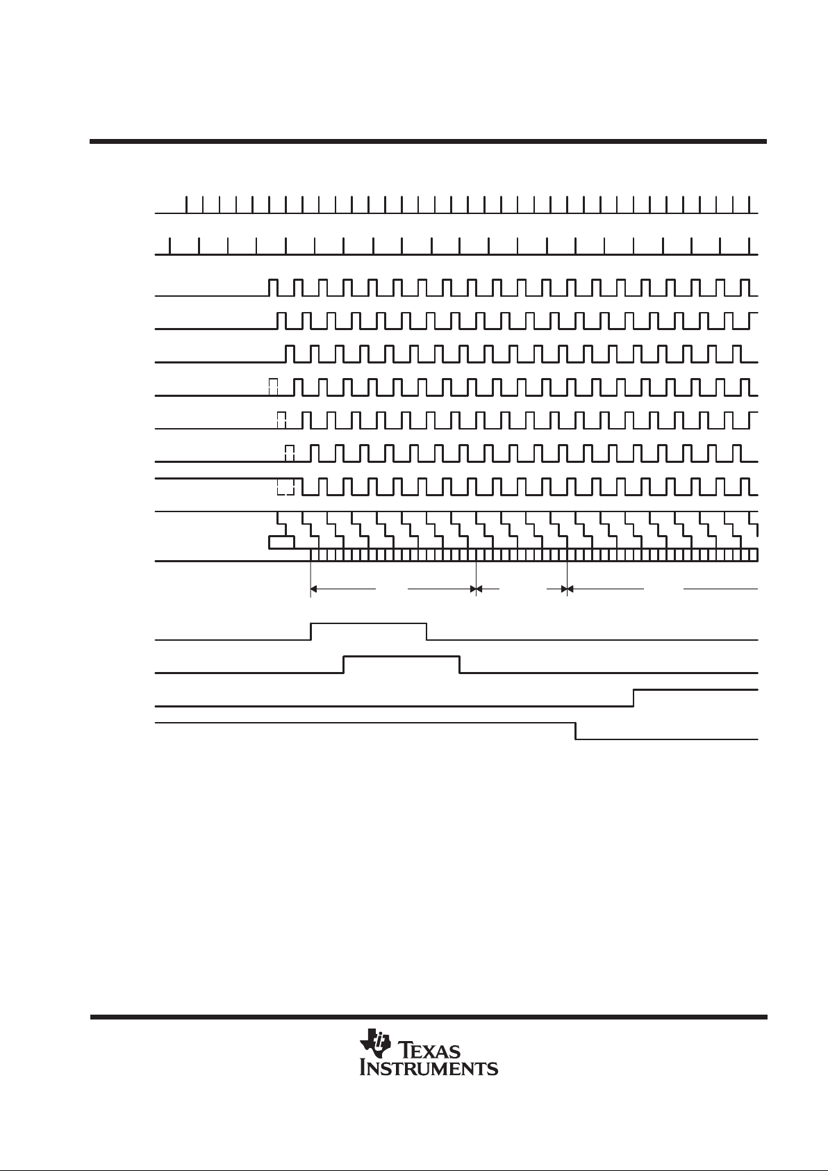
PARAMETER MEASUREMENT INFORMATION
1 Line = 63.55 µs
1 Frame = 525 Lines
(525)
CLK2M
PS,T
ABIN
GT
PI
GT1/SH3
SH1,GT3/SH2,
GT2
S1,S2,S3
SC,SC(90)
HGATE
VGATE
VD2
BCP2
BCP1
BF
CBLK
CSYNC
CP2
CP1
FI
VD
523
521
Continuous
279262
524
9
0
0
Continuous
258.5
27
521
260259
2726
522.5
521.5
EQ
VS
EQ
EQ
VS
EQ
20
0
272
262
9
524
Even Field
Odd Field
0
268.5
262.5
60
288
280275270265260256
302520151050
17
GP
GPS
268.5
262.5
60
Vertical
Scale
†
†
525 intervals equal 33.3 ms equals 1 TV frame
Figure 3. Vertical Timing, Normal-Integration Mode
Page 8

SN28835
1/2-INCH NTSC TIMER
SOCS023B – FEBRUARY 1991
8
POST OFFICE BOX 655303 • DALLAS, TEXAS 75265
PARAMETER MEASUREMENT INFORMATION
GT2
SC,SC(90)
CLK2M
T
PS
S1, S2, S3
HGATE
BCP2
BCP1
BF
CP2
CP1
Horizontal
Scale
†
(130)
Continuous
Continuous
20
14
22
0
133
68
583
123
73
68
83
210
133
70656055
302520151050125
120
4.77273 MHz
4.77273 MHz
4.77273 MHz
35 791113
3579111
13 15
CSYNC
‡
SH1,GT3/SH2,
GT1/SH3
7595
98
Case 1
Case 2
Case 3
CBLK
†
130 intervals equal 63.55 µs equals one horizontal-scan line
‡
CSYNC varies depending on which horizontal-scan line of a 262.5-line TV field is being examined:
• Case 1 depicts the equalizing pulses that occur during horizontal-scan lines 1, 2, 3, 7, 8, and 9.
• Case 2 depicts the vertical serration pulses that occur during horizontal-scan lines 4, 5, and 6.
• Case 3 applies to all remaining horizontal-scan lines.
Figure 4. Horizontal Timing
Page 9
SN28835
1/2-INCH NTSC TIMER
SOCS023B – FEBRUARY 1991
9
POST OFFICE BOX 655303 • DALLAS, TEXAS 75265
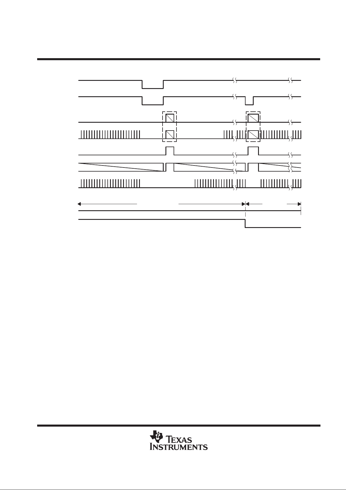
PARAMETER MEASUREMENT INFORMATION
CP2
CBLK
BCP2
BCP1
Y
OUT3
OUT2
OUT1
GT2
GT1/SH3
GT3/SH2
SH1
S3
S2
S1
Horizontal
Scale
‡
Master
Clock
†
(1) : Dummy (2) : Dummy (3) : Half Dark
7654321
140 160150130120110100
23222120191817161514
0
1 2 3 4 5 6 7 8 9 10 11121314151617181920 21 1 2 3 4 5 6 7 8 9 1011121314151617181920 2112345678 9 222324
(1)
3211
(3)
(2)
76543218
Dark Dummy Active
†
910 master-clock periods equal 63.55 µs equals one horizontal-scan line
‡
130 intervals equal 63.55 µs equals one horizontal-scan line
Figure 5. Serial and Sample-and-Hold Timing at Start of Horizontal Transfer
Page 10

SN28835
1/2-INCH NTSC TIMER
SOCS023B – FEBRUARY 1991
10
POST OFFICE BOX 655303 • DALLAS, TEXAS 75265
PARAMETER MEASUREMENT INFORMATION
GT2
GT1/SH3
GT3/SH2
SH1
Late
S1
S2
S3
Early
S3
S2
S1
Horizontal
Scale
†
Acceptable
171615
± 5 ns ± 5 ns
± 5 ns
35 ± 10 ns
± 5 ns
± 5 ns
± 5 ns
± 10 ns
± 5 ns
± 5 ns
± 5 ns
± 5 ns
± 5 ns
± 5 ns
Master
Clock
‡
†
130 intervals equal 63.55 µs equals one horizontal-scan line
‡
910 master-clock periods equal 63.55 µs equals one horizontal-scan line
Figure 6. Timing for S and SH Signals Using Both Early and Late Options
Page 11

SN28835
1/2-INCH NTSC TIMER
SOCS023B – FEBRUARY 1991
11
POST OFFICE BOX 655303 • DALLAS, TEXAS 75265
PARAMETER MEASUREMENT INFORMATION
ABIN Timing at the Start of H
Horizontal
Scale
†
CBLK
BCP1
ABIN
VD
ABIN Timing at the Start of V
1 MHz (always free running)
(130)
26242220181614121086420128126124
ABIN
(mode 0)
ABIN
(mode 1)
ABIN
(mode 2)
ABIN
(mode 3)
(modes 1
or 2)
†
130 intervals equal 63.55 µs equals one horizontal-scan line
NOTE: GPS is high (VD is connected to GP internally)
ANTIBLOOMING-MODE SELECTION
MODE
‡
ABS1 ABS0 ABIN
0 L L Low
1 L H 2-MHz burst
2 H L 1-MHz burst
3 H H 1-MHz free running
‡
In mode 2, the duty cycle is 43%; in all other modes, the duty cycle
is 50%.
Figure 7. Antiblooming Timing at Start of Horizontal Transfer
Page 12

SN28835
1/2-INCH NTSC TIMER
SOCS023B – FEBRUARY 1991
12
POST OFFICE BOX 655303 • DALLAS, TEXAS 75265
PARAMETER MEASUREMENT INFORMATION
V
SS
INLVL
+V
24424312
Odd
244
24424321
12
or 1024
244 or 25621
24424321
(driver output)
DPI
ABIN
GT
PI
PS
T
VD
Vertical-Dump
Frequency
(3.58 MHz
or 2 MHz)
Even
Odd
Even
GP
Figure 8. PI, PS, T, and ABIN Timing
NOTES: A. When the vertical-dump frequency is 2 MHz (chosen by a low level on VDS), the duty cycle of T, PS, and
PI is 4/7 high and 3/7 low; the duty cycle is 50% for a vertical-dump frequency of 3.58 MHz.
B. When GPS is high, VD is connected internally to GP.
C. Neither SC nor SC(90) is used for the 3.58-MHz clock.
D. GP goes low when VD is low. PI, PS, T, and GT begin clocking after VD goes high.
E. The 90° phase shift between T, PS, and PI pulses is equal to one 14-MHz crystal-oscillator clock period.
Page 13

SN28835
1/2-INCH NTSC TIMER
SOCS023B – FEBRUARY 1991
13
POST OFFICE BOX 655303 • DALLAS, TEXAS 75265
PARAMETER MEASUREMENT INFORMATION
Refresh Pulses
PD
ABIN
GT
S1, S2, S3
PS,T
244 Pulses
1024 Pulses
(see Note B)
PI
SB
See Note C
Standby Operation
ABIN
GT
S1, S2, S3
PS,T
244 Pulses1024 Pulses
PI
PD
SB
(see
Note A)
Power
Power-Up Operation
VD (see
Note B)
VD (see
Note D)
GPS
GP
GPS
Refresh Pulses
(see Note B)
GP
Figure 9. Power-Up and Standby Timing
NOTES: A. A 0.1-µF capacitor is connected between SB and GND.
B. In both powerup and standby operation, 1024 refresh pulses are generated on PI, PS, and T even if VD is not connected internally
to GP.
C. When SB
is low, ABIN, GT, PD, PI, PS, S1, S2, S3, and T are all low.
D. VD is connected internally to GP (GPS is high).
Page 14
SN28835
1/2-INCH NTSC TIMER
SOCS023B – FEBRUARY 1991
14
POST OFFICE BOX 655303 • DALLAS, TEXAS 75265
PARAMETER MEASUREMENT INFORMATION
VD
GP
PI
PS,T
GT
ABIN
BCP1, BCP2
Mode
Operation
Variable-Integration-Time
(see Note B)
256 Pulses
(see Note A)
244 Pulses
Operation
GPS
Normal Operation
See Note C
Figure 10. Timing – Normal Operation Versus Variable-Integration-Time Operation
NOTES: A. When VD is low and GP level changes from high to low, 244 pulses are generated on PI, PS, and T.
B. When GP goes low , 256 pulses are generated on PI, PS, and T.
C. Depending on the shutter design, GPS can either be held low or clocked during variable-integration-mode operation.
If GPS is clocked, VD follows GP during the intervals in which GPS is high.
Page 15

SN28835
1/2-INCH NTSC TIMER
SOCS023B – FEBRUARY 1991
15
POST OFFICE BOX 655303 • DALLAS, TEXAS 75265
PARAMETER MEASUREMENT INFORMATION
Operation of VCR
CSYNC
VCR
Internal
Vertical
Counter
(see Note A)
109876
CSYNC
HCR
Horizontal
Scale
†
Operation of HCR
171513119753
Equalization Pulses
Figure 11. Horizontal and Vertical Reset Timing
†
130 intervals equals 63.55 µs equals one horizontal-scan line
NOTE A: The internal vertical counter is preset to the value 6 (indicating the end of vertical sync) when VCR transitions from low to high.
Immediately following the low-to-high transition on VCR, horizontal scanning commences on line 7 of the frame.
SC(90)
SC
Figure 12. SC and SC(90) Timing
Page 16

SN28835
1/2-INCH NTSC TIMER
SOCS023B – FEBRUARY 1991
16
POST OFFICE BOX 655303 • DALLAS, TEXAS 75265
MECHANICAL DATA
FS/S-PQFP-G44 PLASTIC QUAD FLATP ACK
4040160/A–10/93
1,50
1,10
18,20
17,40
33 23
34
44
111
22
12
2,30 MAX
0,10
0,20
1,00 TYP
SQ
14,20 MAX SQ
2,20 MAX
0,55 MAX
0°–10°
Seating Plane
0,10 MIN
0,10
NOTES: A. All linear dimensions are in millimeters.
B. This drawing is subject to change without notice.
Page 17

IMPORTANT NOTICE
T exas Instruments and its subsidiaries (TI) reserve the right to make changes to their products or to discontinue
any product or service without notice, and advise customers to obtain the latest version of relevant information
to verify, before placing orders, that information being relied on is current and complete. All products are sold
subject to the terms and conditions of sale supplied at the time of order acknowledgement, including those
pertaining to warranty, patent infringement, and limitation of liability.
TI warrants performance of its semiconductor products to the specifications applicable at the time of sale in
accordance with TI’s standard warranty. Testing and other quality control techniques are utilized to the extent
TI deems necessary to support this warranty. Specific testing of all parameters of each device is not necessarily
performed, except those mandated by government requirements.
CERT AIN APPLICATIONS USING SEMICONDUCTOR PRODUCTS MAY INVOLVE POTENTIAL RISKS OF
DEATH, PERSONAL INJURY, OR SEVERE PROPERTY OR ENVIRONMENTAL DAMAGE (“CRITICAL
APPLICATIONS”). TI SEMICONDUCTOR PRODUCTS ARE NOT DESIGNED, AUTHORIZED, OR
WARRANTED TO BE SUITABLE FOR USE IN LIFE-SUPPORT DEVICES OR SYSTEMS OR OTHER
CRITICAL APPLICATIONS. INCLUSION OF TI PRODUCTS IN SUCH APPLICA TIONS IS UNDERST OOD TO
BE FULLY AT THE CUSTOMER’S RISK.
In order to minimize risks associated with the customer’s applications, adequate design and operating
safeguards must be provided by the customer to minimize inherent or procedural hazards.
TI assumes no liability for applications assistance or customer product design. TI does not warrant or represent
that any license, either express or implied, is granted under any patent right, copyright, mask work right, or other
intellectual property right of TI covering or relating to any combination, machine, or process in which such
semiconductor products or services might be or are used. TI’s publication of information regarding any third
party’s products or services does not constitute TI’s approval, warranty or endorsement thereof.
Copyright 1998, Texas Instruments Incorporated
 Loading...