Page 1

Application Report
SLOA058– November 2000
A Single-Supply Op-Amp Circuit Collection
Bruce Carter Op-Amp Applications, High Performance Linear Products
One of the biggest problems for designers of op-amp circuitry arises when the circuit must
be operated from a single supply, rather than ±15 V. This application note provides
working circuit examples.
Contents
1 Introduction ................................................................................................................................... 3
1.1 Split Supply vs Single Supply.................................................................................................... 3
1.2 Virtual Ground........................................................................................................................... 4
1.3 AC-Coupling............................................................................................................................. 4
1.4 Combining Op-Amp Stages ...................................................................................................... 5
1.5 Selecting Resistor and Capacitor Values.................................................................................. 5
2 Basic Circuits ................................................................................................................................ 5
2.1 Gain .......................................................................................................................................... 5
2.2 Attenuation ............................................................................................................................... 6
2.3 Summing .................................................................................................................................. 9
2.4 Difference Amplifier .................................................................................................................. 9
2.5 Simulated Inductor.................................................................................................................... 9
2.6 Instrumentation Amplifiers ...................................................................................................... 10
3 Filter Circuits............................................................................................................................... 12
3.1 Single Pole Circuits................................................................................................................. 13
3.1.1 Low Pass Filter Circuits .............................................................................................................13
3.1.2 High Pass Filter Circuits.............................................................................................................13
3.1.3 All-Pass Filter............................................................................................................................14
3.2Double-Pole Circuits............................................................................................................... 15
3.2.1 Sallen-Key.................................................................................................................................15
3.2.2 Multiple Feedback (MFB)...........................................................................................................16
3.2.3 Twin T.......................................................................................................................................17
3.2.4 Fliege........................................................................................................................................20
3.2.5 Akerberg-Mossberg Filter .......................................................................................................... 22
3.2.6 BiQuad...................................................................................................................................... 24
3.2.7 State Variable............................................................................................................................25
4 References................................................................................................................................... 25
Appendix A – Standard Resistor and Capacitor Values ................................................................. 26
Figures
1 Split Supply (L) vs Single Supply (R) Circuits..................................................................................3
2 Single-Supply Operation at Vcc/2 ....................................................................................................4
3 AC-Coupled Gain Stages................................................................................................................6
4 Traditional Inverting Attenuation With an Op Amp...........................................................................6
5 Inverting Attenuation Circuit ............................................................................................................7
6 Noninverting Attenuation.................................................................................................................8
1
Page 2

SLOA058
7 Inverting Summing Circuit............................................................................................................... 9
8 Subtracting Circuit........................................................................................................................... 9
9 Simulated Inductor Circuit............................................................................................................. 10
10 Basic Instrumentation-Amplifier Circuit.......................................................................................... 11
11 Simulated Instrumentation-Amplifier Circuit................................................................................... 11
12 Instrumentation Circuit With Only Two Op Amps...........................................................................12
13 Low-Pass Filter Circuits.................................................................................................................13
14 High-Pass Filter Circuits................................................................................................................ 14
15 All-Pass Filter Circuit.....................................................................................................................14
16 Sallen-Key Low- and High-Pass Filter Topologies......................................................................... 16
17 Multiple-Feedback Topologies.......................................................................................................17
18 Single Op-Amp Twin-T Filter in Band-Pass Configuration............................................................. 18
19 Single Op-Amp Twin-T Filter in Notch Configuration..................................................................... 18
20 Dual-Op-Amp Twin-T Low-Pass Filter...........................................................................................19
21 Dual-Op-Amp Twin-T High-Pass Filter ..........................................................................................19
22 Dual-Op-Amp Twin-T Notch Filter .................................................................................................20
23 Low-Pass Fliege Filter ...................................................................................................................20
24 High-Pass Fliege Filter..................................................................................................................21
25 Band-Pass Fliege Filter.................................................................................................................21
26 Notch Fliege Filter.........................................................................................................................22
27 Akerberg-Mossberg Low-Pass Filter .............................................................................................22
28 Akerberg-Mossberg High-Pass Filter.............................................................................................23
29 Akerberg-Mossberg Band-Pass Filter............................................................................................23
30 Akerberg-Mossberg Notch Filter....................................................................................................24
31 Biquad Low-Pass and Band-Pass Filter ........................................................................................24
32 State-Variable Four-Op-Amp Topology .........................................................................................25
Tables
1 Normalization Factors .....................................................................................................................8
2 A Single-Supply Op-Amp Circuit Collection
Page 3
1 Introduction
There have been many excellent collections of op-amp circuits in the past, but all of them focus
exclusively on split-supply circuits. Many times, the designer who has to operate a circuit from a
single supply does not know how to do the conversion.
Single-supply operation requires a little more care than split-supply circuits. The designer should
read and understand this introductory material.
1.1 Split Supply vs Single Supply
SLOA058
All op amps have two power pins. In most cases, they are labeled V
they are labeled V
and GND. This is an attempt on the part of the data sheet author to
CC
CC+
and V
, but sometimes
CC-
categorize the part as a split-supply or single-supply part. However, it does not mean that the op
amp has to be operated that way—it may or may not be able to operate from different voltage
rails. Consult the data sheet for the op amp, especially the absolute maximum ratings and
voltage-swing specifications, before operating at anything other than the recommended
power-supply voltage(s).
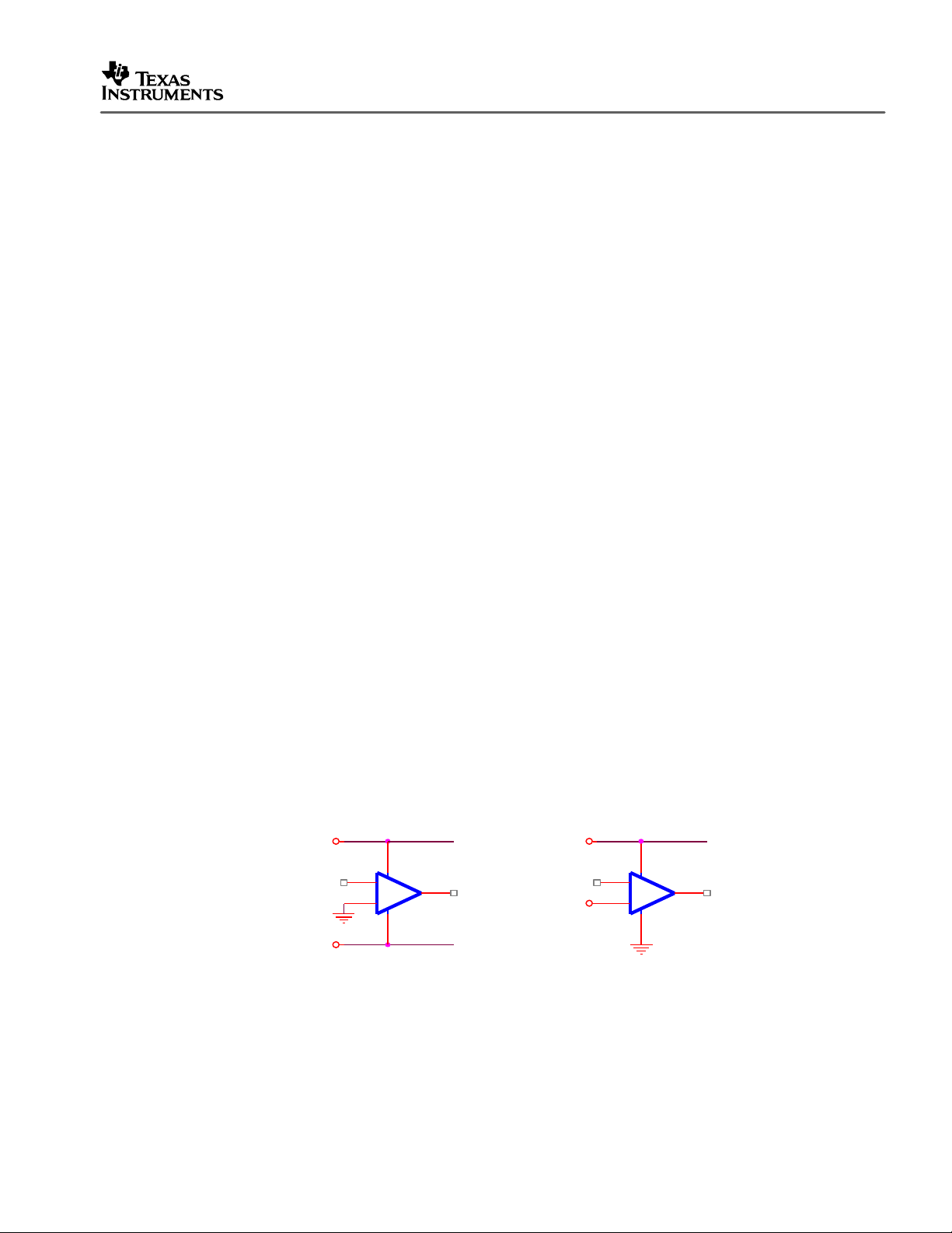
Most analog designers know how to use op amps with a split power supply. As shown in the left
half of Figure 1, a split power supply consists of a positive supply and an equal and opposite
negative supply. The most common values are ±15 V, but ±12 V and ±5 V are also used. The
input and output voltages are referenced to ground, and swing both positive and negative to a
limit of V
, the maximum peak-output voltage swing.
OM±
A single-supply circuit (right side of Figure 1) connects the op-amp power pins to a positive
voltage and ground. The positive voltage is connected to V
, and ground is connected to V
CC+
CC-
or GND. A virtual ground, halfway between the positive supply voltage and ground, is the
reference for the input and output voltages. The voltage swings above and below this virtual
ground to the limit of V
which are specified in data sheets as V
. Some newer op amps have different high- and low-voltage rails,
OM±
OH
and V
respectively. It is important to note that there
OL,
are very few cases when the designer has the liberty to reference the input and output to the
virtual ground. In most cases, the input and output will be referenced to system ground, and the
designer must use decoupling capacitors to isolate the dc potential of the virtual ground from the
input and output (see section 1.3).
+SUPPLY +SUPPLY
-
+
-SUPPLY
-
+
HALF_SUPPLY
Figure 1. Split Supply (L) vs Single Supply (R) Circuits
A common value for single supplies is 5 V, but voltage rails are getting lower, with 3 V and even
lower voltages becoming common. Because of this, single-supply op amps are often rail-to-rail
devices, which avoids losing dynamic range. Rail-to-rail may or may not apply to both the input
and output stages. Be aware that even though a device might be specified as rail-to-rail, some
A Single-Supply Op-Amp Circuit Collection 3
Page 4
SLOA058
Ω
specifications can degrade close to the rails. Be sure to consult the data sheet for complete
specifications on both the inputs and outputs. It is the designer’s obligation to ensure that the
voltage rails of the op amp do not degrade the system specifications.
1.2 Virtual Ground
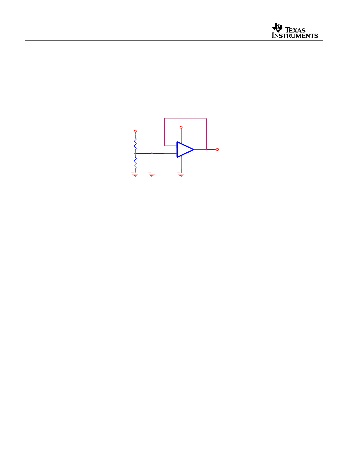
Single-supply operation requires the generation of a virtual ground, usually at a voltage equal to
Vcc/2. The circuit in Figure 2 can be used to generate Vcc/2, but its performance deteriorates at
low frequencies.
R1 and R2 are equal values, selected with power consumption vs allowable noise in mind.
Capacitor C1 forms a low-pass filter to eliminate conducted noise on the voltage rail. Some
applications can omit the buffer op amp.
In what follows, there are a few circuits in which a virtual ground has to be introduced with two
resistors within the circuit because one virtual ground is not suitable. In these instances, the
resistors should be 100 kW or greater; when such a case arises, values are indicated on the
schematic.
1.3 AC-Coupling
A virtual ground is at a dc level above system ground; in effect, a small, local-ground system has
been created within the op-amp stage. However, there is a potential problem: the input source
and output load are probably referenced to system ground, and if the op-amp stage is connected
to a source that is referenced to ground instead of virtual ground, there will be an unacceptable
dc offset. If this happens, the op amp becomes unable to operate on the input signal, because it
must then process signals at and below its input and output rails.
C1
0.1 µF
+Vcc
-
+
Vcc/2
R1
100 k
R2
100 k
+Vcc
Ω
Figure 2. Single-Supply Operation at VCC/2
The solution is to ac-couple the signals to and from the op-amp stage. In this way, the input and
output devices can be referenced to ground, and the op-amp circuitry can be referenced to a
virtual ground.
When more than one op-amp stage is used, interstage decoupling capacitors might become
unnecessary if all of the following conditions are met:
• The first stage is referenced to virtual ground.
• The second stage is referenced to virtual ground.
4 A Single-Supply Op-Amp Circuit Collection
Page 5

• There is no gain in either stage. Any dc offset in either stage is multiplied by the gain in
both, and probably takes the circuit out of its normal operating range.
If there is any doubt, assemble a prototype including ac-coupling capacitors, then remove them
one at a time. Unless the input or output are referenced to virtual ground, there must be an
input-decoupling capacitor to decouple the source and an output-decoupling capacitor to
decouple the load. A good troubleshooting technique for ac circuits is to terminate the input and
output, then check the dc voltage at all op-amp inverting and noninverting inputs and at the
op-amp outputs. All dc voltages should be very close to the virtual-ground value. If they are not,
decoupling capacitors are mandatory in the previous stage (or something is wrong with the
circuit).
1.4 Combining Op-Amp Stages
Combining op-amp stages to save money and board space is possible in some cases, but it
often leads to unavoidable interactions between filter response characteristics, offset voltages,
noise, and other circuit characteristics. The designer should always begin by prototyping
separate gain, offset, and filter stages, then combine them if possible after each individual circuit
function has been verified. Unless otherwise specified, filter circuits included in this document
are unity gain.
SLOA058
1.5 Selecting Resistor and Capacitor Values
The designer who is new to analog design often wonders how to select component values.
Should resistors be in the 1-Ω decade or the 1-MΩ decade? Resistor values in the 1-kΩ to
100-kΩ range are good for general-purpose applications. High-speed applications usually use
resistors in the 100-Ω to 1-kΩ decade, and they consume more power. Portable applications
usually use resistors in the 1-MΩ or even 10-MΩ decade, and they are more prone to noise.
Basic formulas for selecting resistor and capacitor values for tuned circuits are given in the
various figures. For filter applications, resistors should be chosen from 1% E-96 values (see
Appendix A). Once the resistor decade range has been selected, choose standard E-12 value
capacitors. Some tuned circuits may require E-24 values, but they should be avoided where
possible. Capacitors with only 5% tolerance should be avoided in critical tuned circuits—use 1%
instead.
2 Basic Circuits
2.1 Gain
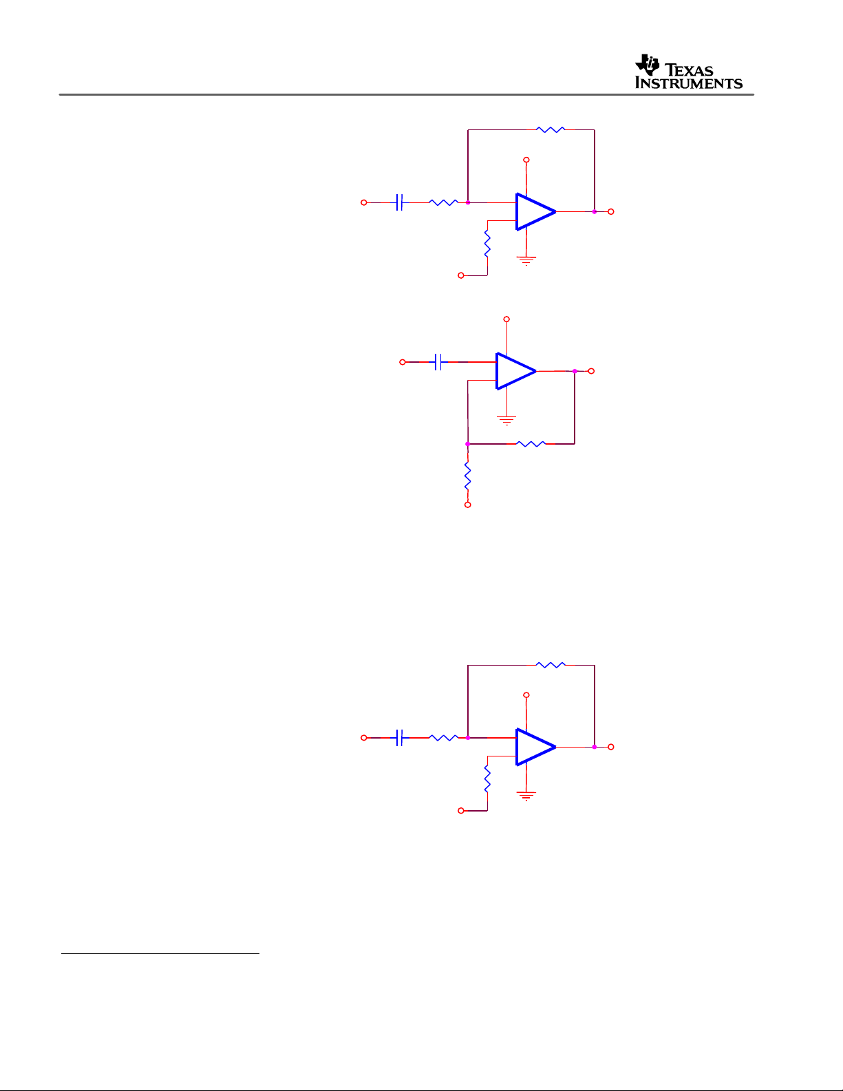
Gain stages come in two basic varieties: inverting and noninverting. The ac-coupled version is
shown in Figure 3. For ac circuits, inversion means an ac-phase shift of 180°. These circuits
work by taking advantage of the coupling capacitor, CIN, to prevent the circuit from having dc
gain. They have ac gain only. If CIN is omitted in a dc system, dc gain must be taken into
account.
It is very important not to violate the bandwidth limit of the op amp at the highest frequency seen
by the circuit. Practical circuits can include gains of 100 (40 dB), but higher gains could cause
the circuit to oscillate unless special care is taken during PC board layout. It is better to cascade
two or more equal-gain stages than to attempt high gain in a single stage.
A Single-Supply Op-Amp Circuit Collection 5
Page 6
SLOA058
+Vcc
Vout
INVERTING
Gain = – R2/R1
R3 = R1||R2
for minimum error due
to input bias current
NONINVERTING
Gain = 1 + R2/R1
Input Impedance = R1||R2
for minimum error due
to input bias current
Vin
Vin
Cin
R1
Vcc/2
Cin
R3
R1
+
-
+Vcc
+
R2
Vout
R2
2.2 Attenuation
The traditional way of doing inverting attenuation with an op-amp circuit is shown in Figure 4, in
INVERTING
Gain = – R2/R1
R3 = R1||R2
for minimum error due
to input bias current
which R2 < R1. This method is not recommended, because many op amps are unstable at gains
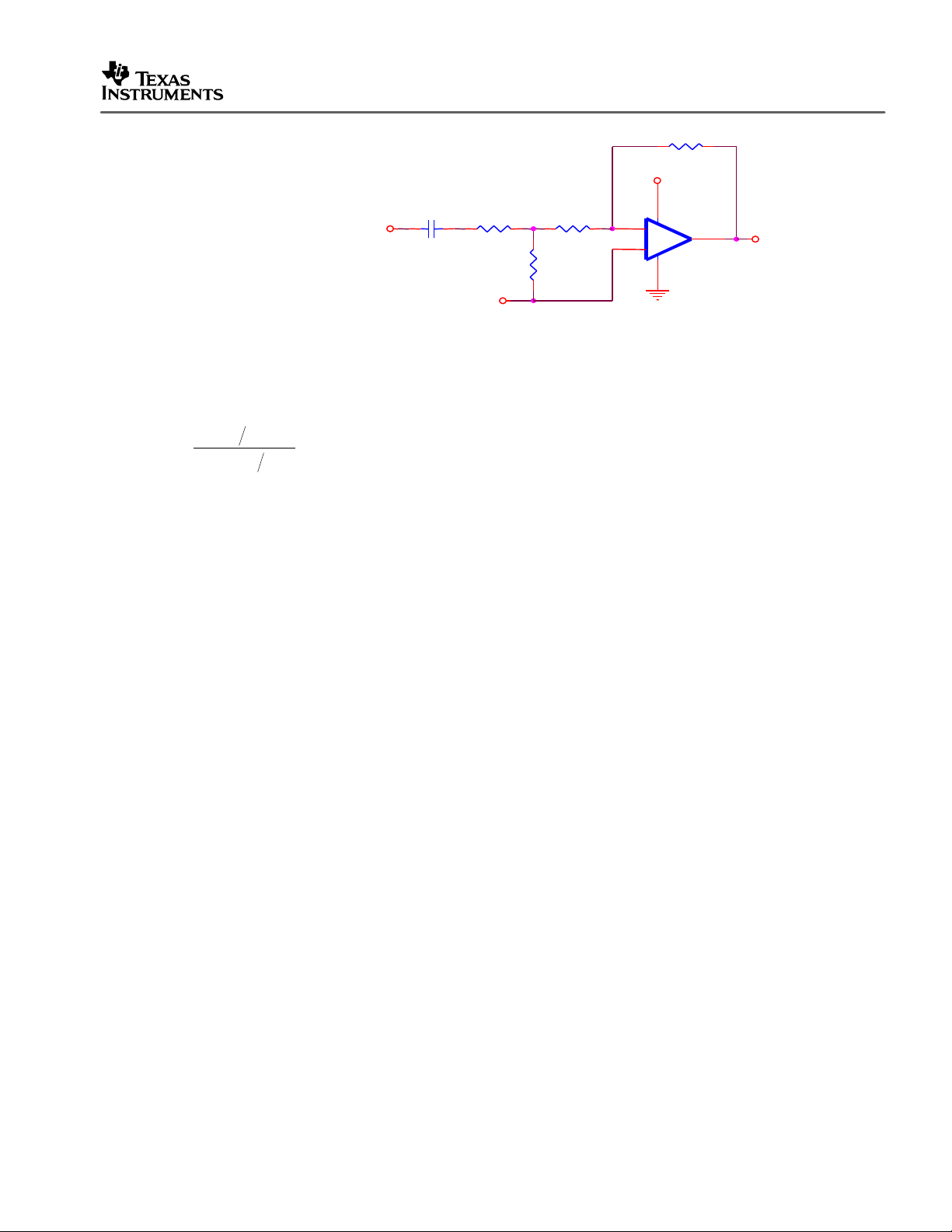
of less than unity. The correct way to construct an attenuation circuit1 is shown in Figure 5.
Vcc/2
Figure 3. AC-Coupled Gain Stages
R2
+Vcc
Cin
Vin
R1
-
+
R3
Vcc/2
Figure 4. Traditional Inverting Attenuation With an Op Amp
Vout
1
This circuit is taken from the design notes of William Ezell
6 A Single-Supply Op-Amp Circuit Collection
Page 7
Rf 2
SLOA058
INVERTING
Component values
normalized to unity
Vin
Cin
Vcc/2
RinA 1
RinB 1
R3
+Vcc
-
+
Vout
Figure 5. Inverting Attenuation Circuit
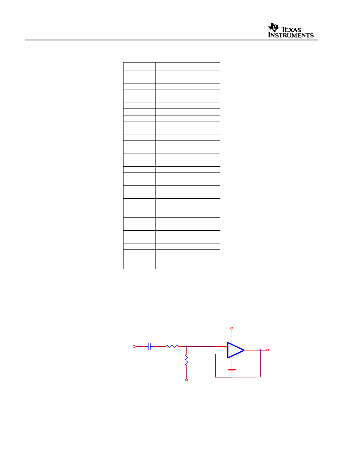
A set of normalized values of the resistor R3 for various levels of attenuation is shown in
Table 1. For nontablated attenuation values, the resistance is:
VV
R
=
INO
( )
VV
223−
INO
To work with normalized values, do the following:
• Select a base-value of resistance, usually between 1 kW and 100 kW for Rf and Rin.
• Divide Rin in two for RinA and RinB.
• Multiply the base value for Rf and Rin by 1 or 2, as shown in Figure 5.
• Look up the normalization factor for R3 in the table below, and multiply it by the base-value
of resistance.
For example, if Rf is 20 kΩ, RinA and RinB are each 10 kΩ, and a 3-dB attenuator would use a
12.1-kΩ resistor.
A Single-Supply Op-Amp Circuit Collection 7
Page 8
SLOA058
0
1.0000
0.5
0.9441
8.4383
1
0.8913
4.0977
2
0.7943
0.9311
2
0.7079
1.2120
3.01
0.7071
1.2071
3.52
0.6667
1.000
4
0.6310
0.8549
5
0.5623
0.6424
6
0.5012
0.5024
6.02
0.5000
0.5000
7
0.4467
0.4036
8
0.3981
0.3307
9
0.3548
0.2750
9.54
0.3333
0.2500
10
0.3162
0.2312
12
0.2512
0.1677
12.04
0.2500
0.1667
13.98
0.2000
0.1250
15
0.1778
0.1081
15.56
0.1667
0.1000
16.90
0.1429
0.08333
18
0.1259
0.07201
18.06
0.1250
0.07143
19.08
0.1111
0.06250
20
0.1000
0.05556
25
0.0562
0.02979
30
0.0316
0.01633
40
0.0100
0.005051
50
0.0032
0.001586
60
0.0010
0.0005005
Vout
Table 1. Normalization Factors
DB Pad Vout/Vin R3
Noninverting attenuation can be performed with a voltage divider and a noninverting buffer as
shown in Figure 6.
NONINVERTING
Component values
normalized to unity
Vin
Figure 6. Noninverting Attenuation
8 A Single-Supply Op-Amp Circuit Collection
Cin
+Vcc
R1
+
-
R2
Vcc/2
Page 9
2.3 Summing
Vout = – R2(Vin1/R1 + Vin2/R2 +
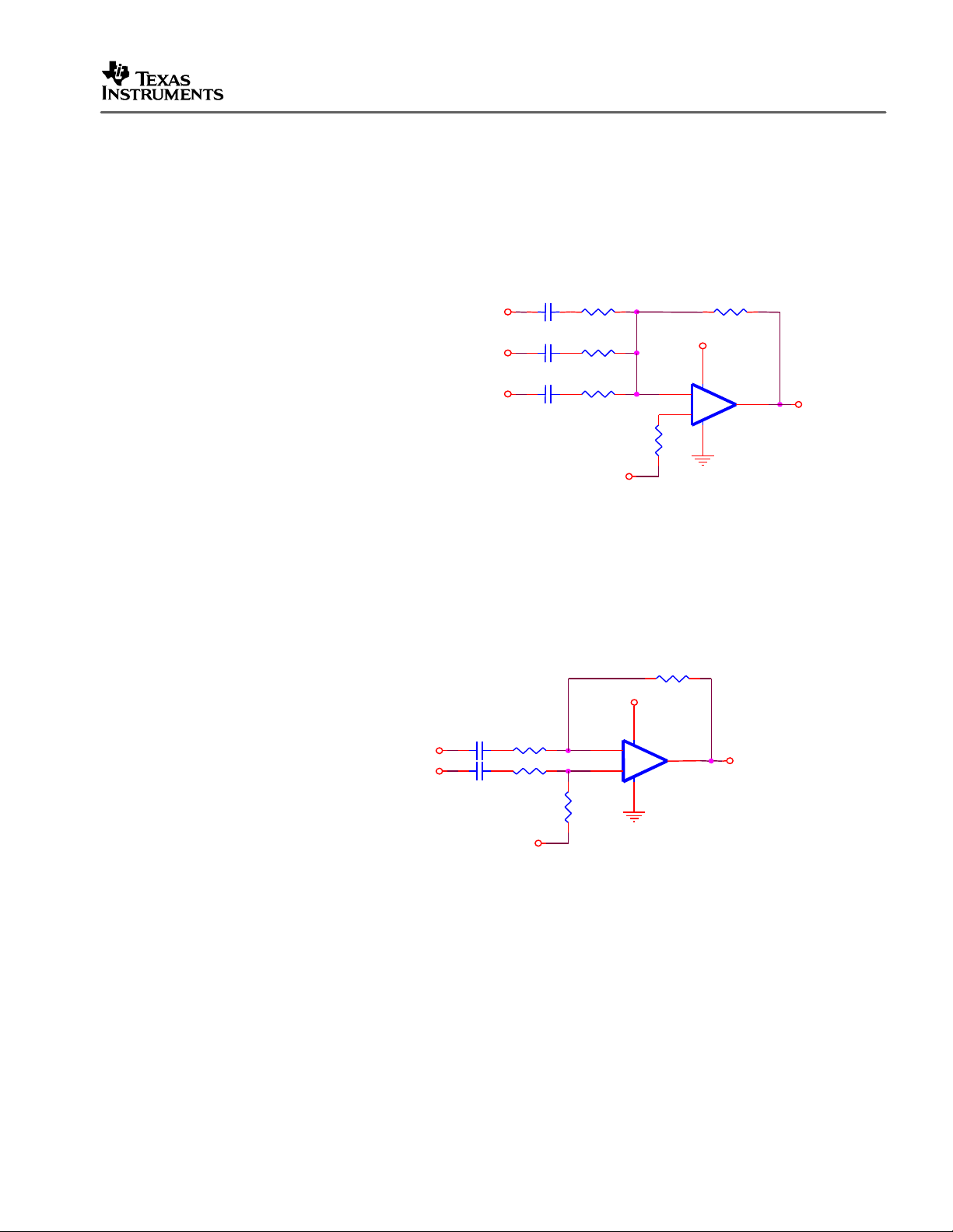
An inverting summing circuit (Figure 7) is the basis of an audio mixer. A single-supply voltage is
seldom used for real audio mixers. Designers will often push an op amp up to, and sometimes
beyond, its recommended voltage rails to increase dynamic range.
Noninverting summing circuits are possible, but not recommended. The source impedance
becomes part of the gain calculation.
SLOA058
INVERTING
Vin3/R3)
= R1A||R1B||R1C||R2
for minimum error due
to input bias current
2.4 Difference Amplifier
Just as there are summing circuits, there are also subtracting circuits (Figure 8). A common
application is to eliminate the vocal track (recorded at equal levels in both channels) from stereo
recordings.
For R1 = R3 and R2 = R4:
Vout = (R2/R1)(Vin2 – Vin1)
R1||R2 = R3||R4
for minimum error due
to input bias current
Vin1
Cin1
Cin2
Vin2
CIin3
Vin3
R1A
R1B
R1C
Vcc/2
Figure 7. Inverting Summing Circuit
Cin1
Vin1
Vin2
Cin2
R1
R3
R4
+Vcc
-
+
R3
R2
+Vcc
-
+
R2
Vout
Vout
2.5 Simulated Inductor
The circuit in Figure 9 reverses the operation of a capacitor, thus making a simulated inductor.
An inductor resists any change in its current, so when a dc voltage is applied to an inductance,
the current rises slowly, and the voltage falls as the external resistance becomes more
significant.
Vcc/2
Figure 8. Subtracting Circuit
A Single-Supply Op-Amp Circuit Collection 9
Page 10

SLOA058
Vout
+Vcc
L = R1*R2*C1
Vin1
C1
Vcc/2
R1
R2
+
-
Figure 9. Simulated Inductor Circuit
An inductor passes low frequencies more readily than high frequencies, the opposite of a
capacitor. An ideal inductor has zero resistance. It passes dc without limitation, but it has infinite
impedance at infinite frequency.
If a dc voltage is suddenly applied to the inverting input through resistor R1, the op amp ignores
the sudden load because the change is also coupled directly to the noninverting input via C1.
The op amp represents high impedance, just as an inductor does.
As C1 charges through R2, the voltage across R2 falls, so the op-amp draws current from the
input through R1. This continues as the capacitor charges, and eventually the op-amp has an
input and output close to virtual ground (Vcc/2).
When C1 is fully charged, resistor R1 limits the current flow, and this appears as a series
resistance within the simulated inductor. This series resistance limits the Q of the inductor. Real
inductors generally have much less resistance than the simulated variety.
There are some limitations of a simulated inductor:
• One end of the inductor is connected to virtual ground.
• The simulated inductor cannot be made with high Q, due to the series resistor R1.
• It does not have the same energy storage as a real inductor. The collapse of the magnetic
field in a real inductor causes large voltage spikes of opposite polarity. The simulated
inductor is limited to the voltage swing of the op amp, so the flyback pulse is limited to the
voltage swing.
2.6 Instrumentation Amplifiers
Instrumentation amplifiers are used whenever dc gain is needed on a low-level signal that would
be loaded by conventional differential-amplifier topologies. Instrumentation amplifiers take
advantage of the high input impedance of noninverting op-amp inputs.
The basic instrumentation amplifier topology is shown in Figure 10.
10 A Single-Supply Op-Amp Circuit Collection
Page 11
+Vcc
SLOA058
Vin-
+
-
R1
R5
R2
+Vcc
ASSUMES Vin- AND Vin+
REFERENCED TO Vcc/2
R1 = R3 (matched)
R2 = R4 (matched)
R5 = R6
R7
+Vcc
-
+
Vout
Gain = R2/R1 (1 + 2R5/R7)
R6
R3
R4
Vcc/2
Vin+
-
+
Figure 10. Basic Instrumentation-Amplifier Circuit
This circuit, and the other instrumentation amplifier topologies presented here, assume that the
inputs are already referenced to half-supply. This is the case with strain gauges that are
operated from Vcc. The basic disadvantage of this circuit is that it requires matched resistors;
otherwise, it would suffer from poor CMRR (see for example, Op Amps for Everyone
[3]
).
The circuit in Figure 10 can be simplified by eliminating three resistors, as shown in Figure 11.
+Vcc
Vin-
+
-
R1
R2
+Vcc
ASSUMES Vin- AND Vin+
REFERENCED TO Vcc/2
R4
-
+
Vout
R1 = R3 (matched)
R2 = R4 (matched)
Gain = R2/R1
Vin+
+Vcc
-
+
R3
Vcc/2
Figure 11. Modified Instrumentation-Amplifier Circuit
A Single-Supply Op-Amp Circuit Collection 11
Page 12

SLOA058
Here, the gain is easier to calculate, but a disadvantage is that now two resistors must be
changed instead of one, and they must be matched resistors. Another disadvantage is that the
first stage(s) cannot be used for gain.
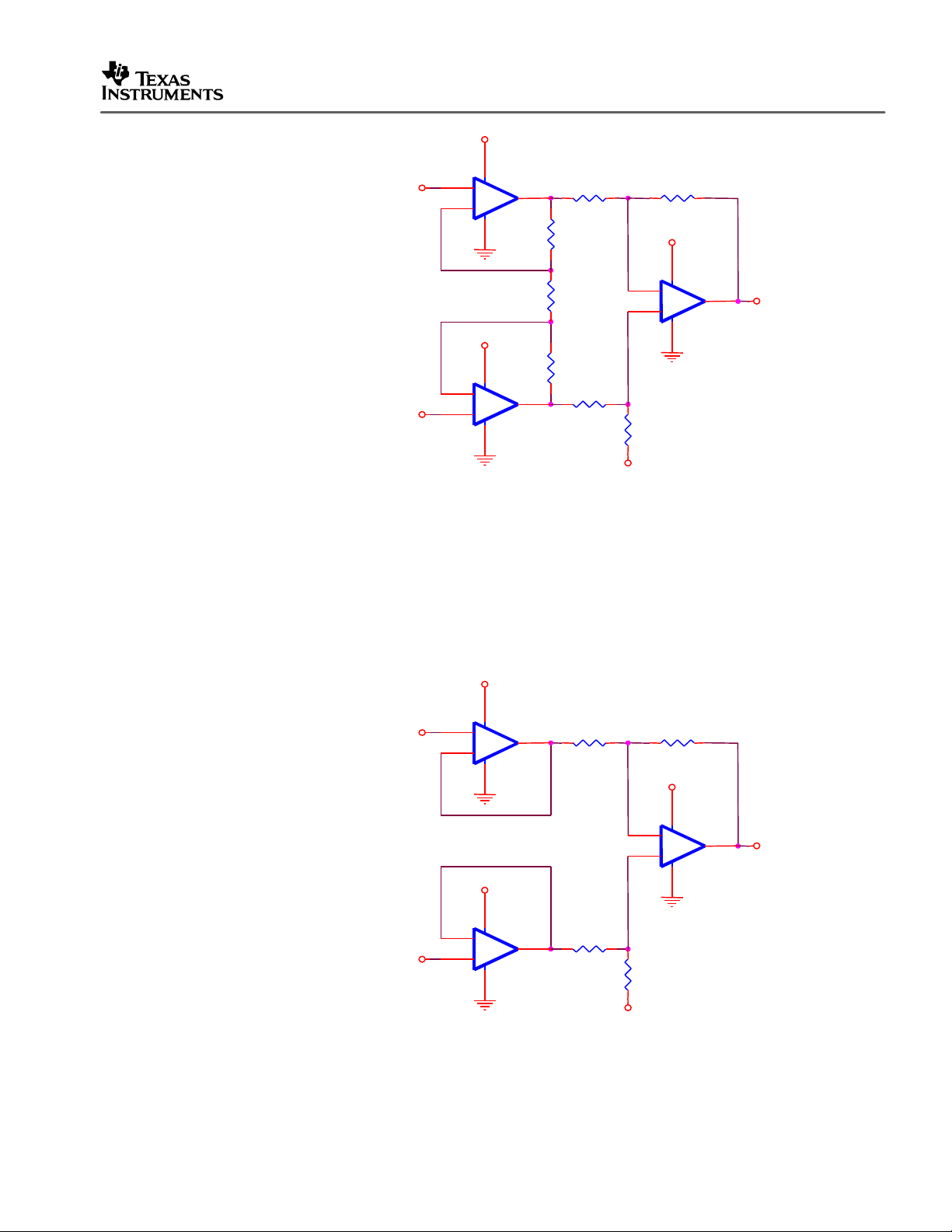
An instrumentation amplifier can also be made from two op amps; this is shown in Figure 12.
ASSUMES Vin- AND Vin+
REFERENCED TO Vcc/2
R1 = R4 (matched)
R2 = R3 (matched)
Gain = 1 + R1/R2
However, this topology is not recommended because the first op amp is operated at less than
unity gain, so it may be unstable. Furthermore, the signal from Vin- has more propagation delay
than Vin+.
3 Filter Circuits
This section is devoted to op-amp active filters. In many cases, it is necessary to block dc
voltage from the virtual ground of the op-amp stage by adding a capacitor to the input of the
circuit. This capacitor forms a high-pass filter with the input so, in a sense, all these circuits have
a high-pass characteristic. The designer must insure that the input capacitor is at least 100 times
the value of the other capacitors in the circuit, so that the high-pass characteristic does not come
into play at the frequencies of interest in the circuit. For filter circuits with gain, 1000 times might
be better. If the input voltage already contains a Vcc/2 offset, the capacitor can be omitted.
R4R2
+Vcc
-
+
Vcc/2
R1
Vin -
R3
+Vcc
-
+
Vin+
Figure 12. Instrumentation Circuit With Only Two Op Amps
Vout
These circuits will have a half-supply dc offset at their output. If the circuit is the last stage in the
system, an output-coupling capacitor may also be required.
There are trade-offs involved in filter design. The most desirable situation is to implement a filter
with a single op amp. Ideally, the filter would be simple to implement, and the designer would
have complete control over:
• The filter corner / center frequency
• The gain of the filter circuit
• The Q of band-pass and notch filters, or style of low-pass and high-pass filter (Butterworth,
Chebyshev, or Bessell).
12 A Single-Supply Op-Amp Circuit Collection
Page 13

Unfortunately, such is not the case—complete control over the filter is seldom possible with a
single op amp. If control is possible, it frequently involves complex interactions between passive
components, and this means complex mathematical calculations that intimidate many designers.
More control usually means more op amps, which may be acceptable in designs that will not be
produced in large volumes, or that may be subject to several changes before the design is
finalized. If the designer needs to implement a filter with as few components as possible, there
will be no choice but to resort to traditional filter-design techniques and perform the necessary
calculations.
3.1 Single Pole Circuits
Single-pole circuits are the simplest filter circuits. They have a roll off of 20 dB per decade.
3.1.1 Low Pass Filter Circuits
Typical low-pass filter circuits are shown in Figure 13.
SLOA058
INVERTING
Fo = 1/(2pR2C1)
Gain = – R2/R1
NONINVERTING
Fo = 1/(2pR1C1)
Gain = 1 + R3/R2
Vin
Vin
Cin
Cin
Vcc/2
R1
R1
C1
Vcc/2
R2
R2
+Vcc
+
+Vcc
C1
Vout
+
-
R3
Vout
3.1.2 High Pass Filter Circuits
Typical high-pass filter circuits are shown in Figure 14.
Figure 13. Low-Pass Filter Circuits
A Single-Supply Op-Amp Circuit Collection 13
Page 14

SLOA058
NONINVERTING
Gain = 1
Fo = 1/(2pR1C1)
NONINVERTING
Fo = 1/(2pR1C1)
Gain = 1 + R3/R2
Vin
Vin
Vcc/2
C1
C1
R1
Vcc/2
R1
R2
+Vcc
+
-
+Vcc
Vout
+
-
R3
Vout
3.1.3 All-Pass Filter
The all-pass filter passes all frequencies at the same gain. It is used to change the phase of the
signal, and it can also be used as a phase-correction circuit. The circuit shown in Figure 15 has
a 90° phase shift at F(90). At dc, the phase shift is 0°, and at high frequencies it is 180°.
R1 = R2 = R3 = R
F(90) = 1/(2pR*C1)
Figure 14. High-Pass Filter Circuits
+Vcc
C1
Vin1
R2
Vcc/2
R1
+
-
Figure 15. All-Pass Filter Circuit
Vout
R3
14 A Single-Supply Op-Amp Circuit Collection
Page 15

3.2 Double-Pole Circuits
Double-pole op-amp circuit topologies are sometimes named after their inventor. Several
implementations or topologies exist. Some double-pole circuit topologies are available in a
low-pass, high-pass, band-pass, and notch configuration. Others are not. Not all topologies and
implementations are given here: only the ones that are easy to implement and tune.
Double-pole or second-order filters have a 40-dB-per-decade roll-off.
Commonly the same component(s) adjust the Q for the band-pass and notch versions of the
topology, and they change the filter from Butterworth to Chebyshev, etc. for low-pass and highpass versions of the topology. Be aware that the corner frequency calculation is only valid for the
Butterworth versions of the topologies. Chebyshev and Bessell modify it slightly.
When band-pass and notch filter circuits are shown, they are high-Q (single frequency) types. To
implement a wider band-pass or notch (band-reject) filter, cascade low-pass and high-pass
stages. The pass characteristics should overlap for a band-pass and not overlap for a
band-reject filter.
Inverse Chebyshev and Elliptic filters are not shown. These are beyond the scope of a circuit
collection note.
Not all filter topologies produce ideal results—the final attenuation in the rejection band, for
example, is greater in the multiple-feedback filter configuration than it is in the Sallen-Key filter.
These fine points are beyond the scope of an op-amp circuit collection. Consult a textbook on
filter design for the merits and drawbacks of each of these topologies. Unless the application is
particularly critical, all the circuits shown here should produce acceptable results.
SLOA058
3.2.1 Sallen-Key
The Sallen-Key topology is one of the most widely-known and popular second-order topologies.
It is low cost, requiring only a single op amp and four passive components to accomplish the
tuning. Tuning is easy, but changing the style of filter from Butterworth to Chebyshev is not. The
designer is encouraged to read references [1] and [2] for a detailed description of this topology.
The circuits shown are unity gain—changing the gain of a Sallen-Key circuit also changes the
filter tuning and the style. It is easiest to implement a Sallen-Key filter as a unity gain
Butterworth.
A Single-Supply Op-Amp Circuit Collection 15
Page 16

SLOA058
LOW PASS
Unity Gain
Butterworth
R3 = R4 (HIGH)
R1 = R2
C1 = 2C2
Fo = √2 / (4pR1C2)
Vin
Cin
R4
+Vcc
R3
R1
R2
C2
C1
+Vcc
+
-
Vout
HIGH PASS
Unity Gain
Butterworth
Vin
C1 = C2
R1 = R
R = 2R1
Fo = √2 / (4pR1C1)
Figure 16. Sallen-Key Low- and High-Pass Filter Topologies
3.2.2 Multiple Feedback (MFB)
MFB topology is very versatile, low cost, and easy to implement. Unfortunately, calculations are
somewhat complex, and certainly beyond the scope of this circuit collection. The designer is
encouraged to read reference [1] for a detailed description of the MFB topology. If all that is
needed is a unity gain Butterworth, then these circuits will provide a close approximation.
C1
C2
R2
Vcc/2
R1
+Vcc
+
-
Vout
16 A Single-Supply Op-Amp Circuit Collection
Page 17

SLOA058
LOW PASS
Unity Gain Butterworth
Fo = 1/(2πRC)
R1 = R2 = R/√2
R3 = R/(2√2)
C1 = C
C2 = 4C
HIGH PASS
Unity Gain Butterworth
Fo = 1/(2πRC)
R1 = 0.47R
R2 = 2.1R
C1 = C2 = C3 = C
BAND PASS
Gain = 2.3 dB
Fo = 1/(2.32πRC)
R1 = 10R
R2 = 0.001R
R3 = 100R
C1 = 10C
C2 = C
Vin
Vin
Vin
Cin
C1
Cin
Vcc/2
Vcc/2
Vcc/2
R1
C2
R1
R1
R2
C2
C1
R2
R3
C3
C2
C1
R2
R3
+Vcc
-
+
+Vcc
-
+
+Vcc
-
+
Vout
Vout
Vout
3.2.3 Twin T
The twin-T topology uses either one or two op amps. It is based on a passive (RC) topology that
uses three resistors and three capacitors. Matching these six passive components is critical;
fortunately, it is also easy. The entire network can be constructed from a single value of
resistance and a single value of capacitance, running them in parallel to create R3 and C3 in the
twin-T schematics shown in Figure. Components from the same batch are likely to have very
similar characteristics.
Figure 17. Multiple-Feedback Topologies
A Single-Supply Op-Amp Circuit Collection 17
Page 18

SLOA058
3.2.3.1 Single Op-Amp Implementations
R2
C2
BAND PASS
R1
C1
C3
Vcc/2
R3
R1 = R2 = R
C1 = C2 = C
R3 = R/2
Vin
Cin
+Vcc
C3 = 2C
Fo = 1/(2pRC)
Gain controlled by R4 and R5
R4 > 100 * R5
R4
-
+
Vout
Q hard to control; need mismatched
Resistors; also affects gain
R5
Vcc/2
Figure 18. Single Op-Amp Twin-T Filter in Band-Pass Configuration
The bandpass circuit will oscillate if the components are matched too closely. It is best to
de-tune it slightly, by selecting the resistor to virtual ground to be one E-96 1% resistor value off,
for instance.
+Vcc
R3
C3
C2
R2
+Vcc
+
-
Vout
NOTCH
C1 = C2 = C
C3 = 2C
R1 = R2 = R
Vin
R3 = R/2
Fo = 1/(2pRC)
R4 = R5: HIGH
The only control over Q
is by mismatching R3
Cin
R5
C1
R4
Vcc/2
R1
Figure 19. Single Op-Amp Twin-T Filter in Notch Configuration
18 A Single-Supply Op-Amp Circuit Collection
Page 19

3.2.3.2 Dual-Op-Amp Implementations
Typical dual op-amp implementations are shown in Figures 20 to 22
SLOA058
LOW PASS
R1 = R2 = R
C1 = C2 = C
R3 = R/2
C3 = 2C
Fo = 1/(2pRC)
Vin
Unity Gain
R4 < R5/2 Chebyshev
R4 = R5/2 Butterworth
R4 > R5/2 Bessel
R6 = R7: HIGH
Figure 20. Dual-Op-Amp Twin-T Low-Pass Filter
Cin
Vcc/2
+Vcc
R7
R6
R1
C1
R3
C3
C2
R2
+Vcc
-
+
+Vcc
Vout
+Vcc
R4
-
+
R5
Vcc/2
HIGH PASS
R1 = R2 = R
C1 = C2 = C
R3 = R/2
C3 = 2C
Fo = 1/(2pRC)
Unity Gain
R4 < R5/2 Chebyshev
R4 = R5/2 Butterworth
R4 > R5/2 Bessel
Figure 21. Dual-Op-Amp Twin-T High-Pass Filter
Vcc/2
Vin
C1
R3
C3
C2
R2R1
+
-
Vout
+Vcc
R4
-
+
R5
Vcc/2
A Single-Supply Op-Amp Circuit Collection 19
Page 20

SLOA058
NOTCH
R1 = R2 = R
C1 = C2 = C
R3 = R/2
C3 = 2C
Fo = 1/(2pRC)
R6 = R7 > 20*R
Q controlled by
ratio of R5 and R4
R4 = 0.05*R5: high Q
R4 = 0.5*R5 low: Q
3.2.4 Fliege
Vin
+Vcc
R6
CIN
R1
R7
C1
R2
C3
R3
C2
Figure 22. Dual-Op-Amp Twin-T Notch Filter
+Vcc
-
+
+Vcc
Vout
R4
-
+
R5
Vcc/2
Fliege is a two-op-amp topology (Figures 23–26), and therefore more expensive than one-opamp topologies. There is good control over the tuning and the Q and style of filter. The gain is
fixed at two for low-pass, high-pass, and band-pass filters, and unity for notch.
+Vcc
LOW PASS
R2 = R3 = R
Cin
Vin
R2
R1
C1
+
-
Vout
C1 = C2 = C
R4 = R5, not critical
R3
Fo = 1/(2pRC)
Gain fixed at 2
+Vcc
C2
R1 = R/√2 Butterworth
R1 > R/√2 Chebyshev
R1 < R/√2 Bessel
-
+
Vcc/2
R4
R5
Figure 23. Low-Pass Fliege Filter
20 A Single-Supply Op-Amp Circuit Collection
Page 21

HIGH PASS
R2 = R3 = R
C1 = C2 = C
R4 = R5, not critical
Fo = 1/(2pRC)
Gain fixed at 2
R1 = R/√2 Butterworth
R1 > R/√2 Chebyshev
R1 < R/√2 Bessel
C1
Vin
R1
Vcc/2
R2
C2
+Vcc
-
+
Figure 24. High-Pass Fliege Filter
Vcc/2
R5
+Vcc
+
-
SLOA058
Vout
R3
R4
BAND PASS
Gain fixed at 2
R1 controls Q
low R1 => low Q
high R1 => high Q
R1 should be > R/5
R2 = R3 = R
C1 = C2 = C
R4 = R5, not critical
Fo = 1/(2pRC)
Cin
Vin
R1
C1
R2
Vcc/2
Figure 25. Band-Pass Fliege Filter
C2
+Vcc
+Vcc
+
-
R3
-
+
Vcc/2
R4
R5
Vout
A Single-Supply Op-Amp Circuit Collection 21
Page 22

SLOA058
+Vcc
Cin
NOTCH
Vin
R3 = R4 = R5 = R6 = R
C1 = C2 = C
Fo = 1/(2pRC)
R1 = R2 = R*10/√2
No control over Q
Gain fixed at 1
3.2.5 Akerberg-Mossberg Filter
This is the easiest of the three-op-amp topologies to use (Figures 27–30). It is easy to change
the gain, style of low-pass and high-pass filter, and the Q of band-pass and notch filters. The
notch filter performance is not as good as that of the twin T notch, but it is less critical.
C1
R1
R2
Vcc/2
R3
C2
R6
+Vcc
-
+
Figure 26. Notch Fliege Filter
+
-
R4
R5
Vout
LOW PASS
R2 = R3 = R4 = R5 = R
C1 = C2 = C
Fo = 1/(2pRC)
Unity Gain: R = R1
Other Gain: R/R1
Cin
Vin
R6 = R/√2 Butterworth
R6 > R/√2 Chebyshev
R6 < R/√2 Bessel
R5
+Vcc
C1
+Vcc
R1
+
-
Vcc/2
R2
-
+
Vcc/2
R3
R4
Vcc/2
Figure 27. Akerberg-Mossberg Low-Pass Filter
R6
+Vcc
C2
-
+
Vout
22 A Single-Supply Op-Amp Circuit Collection
Page 23

SLOA058
HIGH PASS
R2=R3=R4=R5=R
C2=C3=C
Fo=1/(2pRC)
R6 = R/√2 Butterworth
R6 > R/√2 Chebyshev
R6 < R/√2 Bessel
Unity Gain:
C1=C, R1=R
Other Gain:
R1/R AND C1/C
BAND PASS
R2 = R3 = R4 = R5 = R
C1 = C2 = C
Fo = 1/(2pRC)
Unity Gain:
R1 = R6
Other Gain:
– R6/R1
R1, R6 also control Q
low values, low Q
high values, high Q
R5
Vcc/2
Vcc/2
Vcc/2
C2
+Vcc
+
-
+Vcc
R2
-
+
Vcc/2
Vin
R1
R3
R4
C1
Figure 28. Akerberg-Mossberg High-Pass Filter
+Vcc
C1
+Vcc
+
-
Vcc/2
R2
-
+
Cin
R3
R4
Vcc/2
R1
Vcc/2
Vin
R5
R6
+Vcc
R6
+Vcc
-
+
-
+
C3
Vout
C2
Vout
Figure 29. Akerberg-Mossberg Band-Pass Filter
A Single-Supply Op-Amp Circuit Collection 23
Page 24

SLOA058
NOTCH
R1=R2=R3=R4=R5=R6=R
C1 = C2 = C3 = C
Fo = 1/(2πRC)
R/2 < R7 < 2 x R
R7 controls Q
low value, low Q
high value, high Q
3.2.6 BiQuad
Biquad is a well know topology (Figure 31). It is only available in low-pass and band-pass
varieties. The low-pass filter is useful whenever simultaneous normal and inverted outputs are
needed.
Vin
Cin
R1
C1
Vcc/2
+Vcc
+
-
+Vcc
C3
R2
+
Vcc/2
R6
R3
R4
Figure 30. Akerberg-Mossberg Notch Filter
Vcc/2
Vcc/2
R5
R7
+Vcc
C2
-
+
Vout
R4
+Vcc
Cin
R3
-
+
Vcc/2
LOW PASS
R1 = R2 = R
R5 = R6, not critical
R4 = R/√2
C1 = C2 = C
Fo = 1/(2pRC)
R4 = R/√2 Butterworth
R4 > R/√2 Chebyshev
R4 < R/√2 Bessell
Unity Gain: R3 = R
Other Gain: – R/R3
V
BPout
R1
R2
C2C1
+Vcc
V
+LPout
R5
-
+
BAND PASS
R1 = R2 = R5 = R
R6 = about R/√2, not critical
C1 = C2 = C
Fo = 1/(2pRC)
R3 = R4 unity gain
Gain = – R4/R3
R4 also controls Q
low value, low Q
high value, high Q
+Vcc
R6
+
V
–LPout
Figure 31. Biquad Low-Pass and Band-Pass Filter
24 A Single-Supply Op-Amp Circuit Collection
Page 25

3.2.7 State Variable
State variable is a three to four op-amp topology. The fourth op-amp is only required for notch
filters. It is also very easy to tune, and it is easy to change the style of lowpass and highpass,
and easy to change the Q of the bandpass and notch. Unfortunately, it is not as nice a topology
as Akerberg-Mossberg. The same resistor is used for gain and style of filter / Q, limiting control
of the filter. There is probably not a lot of reason to use this topology, unless simultaneous
lowpass, highpass, bandpass, and notch outputs are required by the application.
SLOA058
R5
+Vcc
Cin
Vin
R1=R2=R3=R4=R5=R6=R8=R9=R10=R
C1 = C2 = C
Fo = 1/(2πRC)
R1
R6
Vcc/2
-
+
R7
R2
+Vcc
R3
-
+
Vcc/2
Unity Gain: R7 = R
Other Gain: – R7/R
BP and NOTCH
R7 high value, high Q
R7 low value, low Q
C1
R4
Vcc/2
BPoutHPout
C2
+Vcc
-
+
R9
LP and HP
R7 = R/2 Butterworth
R7 > R/2 Chebyshev
R7 < R/2 Bessel
Figure 32. State-Variable Four-Op-Amp Topology
LPout
R10
+Vcc
R8
-
+
Vcc/2
NOTCH
R8, R9 ,R10 and 4th
op amp only used
for notch
4 References
1. Active Low Pass Filter Design, Texas Instruments Application Report, Literature Number
SLOA049
2. Analysis Of The Sallen-Key Architecture, Texas Instruments Application Report,
Literature Number SLOA024A.
3. Op Amps for Everyone, Ron Mancini (Ed.), Chapter 12, Texas Instruments Literature
Number SLOD006
A Single-Supply Op-Amp Circuit Collection 25
Page 26

SLOA058
Appendix A – Standard Resistor and Capacitor Values
E-12 Resistor / Capacitor Values
1.0, 1.2, 1.5, 1.8, 2.2, 2.7, 3.3, 3.9, 4.7, 5.6, 6.8, and 8.2; multiplied by the decade value.
E-24 Resistor / Capacitor Values
1.0, 1.1, 1.2, 1.3, 1.5, 1.6, 1.8, 2.0, 2.2, 2.4, 2.7, 3.0, 3.3, 3.6, 3.9, 4.3, 4.7, 5.1, 5.6, 6.2, 6.8, 7.5,
8.2, and 9.1; multiplied by the decade value.
E-96 Resistor / Capacitor Values
1.00, 1.02, 1.05, 1.07, 1.10, 1.13, 1.15, 1.18, 1.21, 1.24, 1.27, 1.30, 1.33, 1.37, 1.40, 1.43, 1.47,
1.50, 1.54, 1.58, 1.62, 1.65, 1.69, 1.74, 1.78, 1.82, 1.87, 1.91, 1.96, 2.00, 2.05, 2.10, 2.15, 2.21,
2.26, 2.32, 2.37, 2.43, 2.49, 2.55, 2.61, 2.67, 2.74, 2.80, 2.87, 2.94, 3.01, 3.09, 3.16, 3,24, 3.32,
3.40, 3,48, 3.57, 3.65, 3.74, 3.83, 3.92, 4.02, 4.12, 4.22, 4,32, 4.42, 4,53, 4.64, 4.75, 4.87, 4.99,
5.11, 5.23, 5.36, 5.49, 5.62, 5.76, 5.90, 6.04, 6.19, 6.34, 6.49, 6.65, 6.81, 6.98, 7.15, 7.32, 7.50,
7.68, 7.87, 8.06, 8.25, 8.45, 8.66, 8.87, 9.09, 9.31, 9.53, 9.76; multiplied by the decade value.
26 A Single-Supply Op-Amp Circuit Collection
Page 27

IMPORTANT NOTICE
T exas Instruments and its subsidiaries (TI) reserve the right to make changes to their products or to discontinue
any product or service without notice, and advise customers to obtain the latest version of relevant information
to verify, before placing orders, that information being relied on is current and complete. All products are sold
subject to the terms and conditions of sale supplied at the time of order acknowledgment, including those
pertaining to warranty, patent infringement, and limitation of liability.
TI warrants performance of its semiconductor products to the specifications applicable at the time of sale in
accordance with TI’s standard warranty. Testing and other quality control techniques are utilized to the extent
TI deems necessary to support this warranty . Specific testing of all parameters of each device is not necessarily
performed, except those mandated by government requirements.
Customers are responsible for their applications using TI components.
In order to minimize risks associated with the customer’s applications, adequate design and operating
safeguards must be provided by the customer to minimize inherent or procedural hazards.
TI assumes no liability for applications assistance or customer product design. TI does not warrant or represent
that any license, either express or implied, is granted under any patent right, copyright, mask work right, or other
intellectual property right of TI covering or relating to any combination, machine, or process in which such
semiconductor products or services might be or are used. TI’s publication of information regarding any third
party’s products or services does not constitute TI’s approval, warranty or endorsement thereof.
Copyright 2000, Texas Instruments Incorporated
 Loading...