

Page 1

1 Introduction
The SN65HVS880 evaluation module (EVM) supports the parametric evaluation of the SN65HVS880
digital input serializer. It is intended to be used in conjunction with the SN65HVS880 data sheet,
(SLAS252 ).
Note: this EVM is not intended for electromagnetic compatibility (EMC) tests.
2 EVM Schematic and Layout
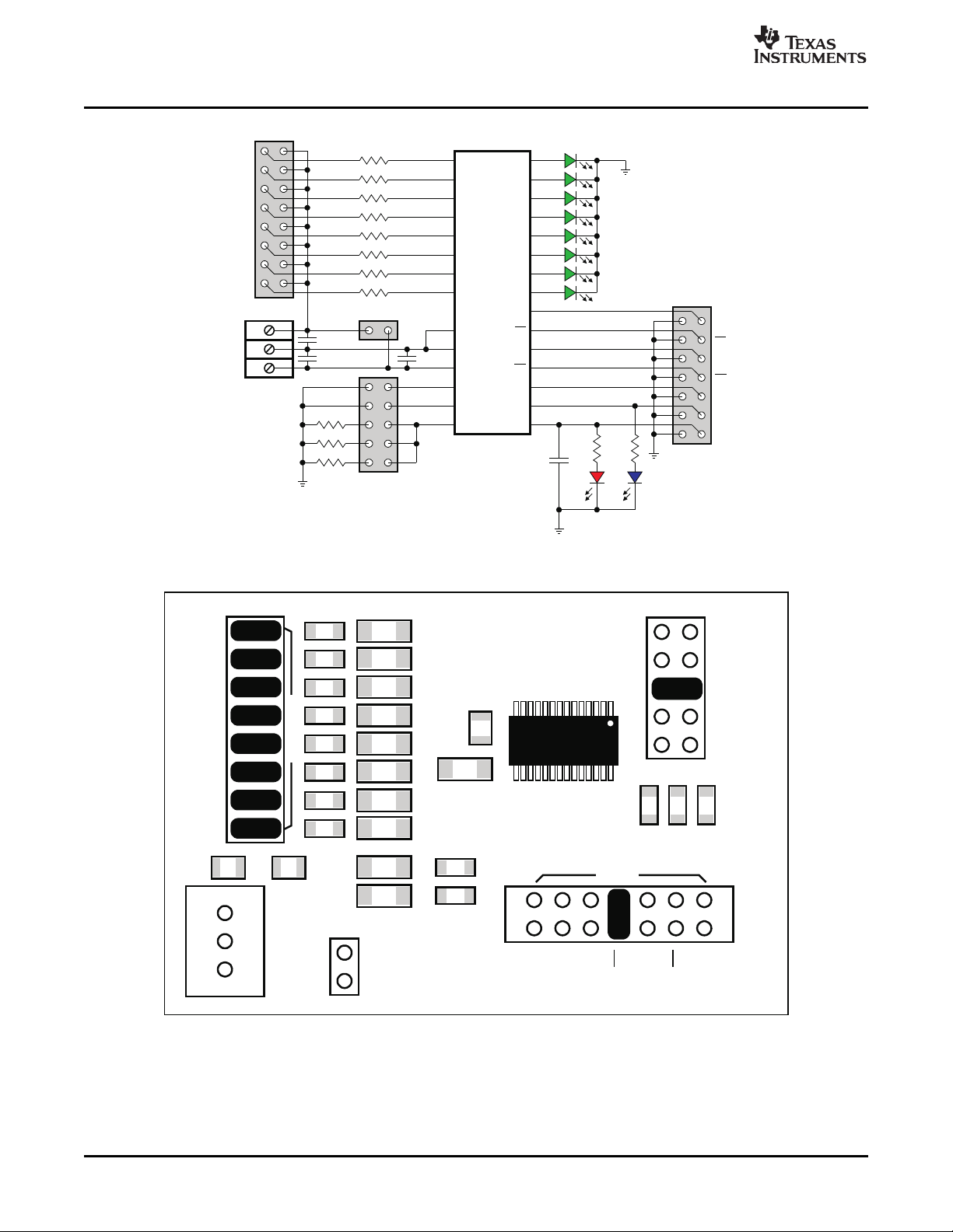
Figure 1 shows the board circuit schematic, and Figure 2 shows the board layout top view. The board
includes a terminal block, TB1, and four connectors, JMP1 to 4.
TB1 receives the board supply of 24V nominal. V24 supplies the SN65HVS880 device, and VFIELD
provides the supply for sensor switches.
Upon the application of V24, the blue Chip-Okay LED (CHOK) indicates proper board function. At the
same time, the red LED indicates 5V availability at the regulator output 5VOP.
JMP1 provides the field inputs IN0:IN7 for field voltages of 24V nominal. They can be applied via:
a. an external supply in series to a sensor switch connected to a field input,
b. or a sensor switch connected between and input and VFIELD,
c. or a direct connection between an input and VFIELD.
In all three cases, a 24V level represents the ON-status of a sensor switch, which is indicated by the
corresponding LEDs D0:D7.
JMP2 provides access to the control and data lines of the internal serializer. To operate the serializer, CE
must be connected either to ground or to CLK.
Upon an active-low load pulse, (a high-to-low-to-high transition) at LD, the status information of the field
inputs is latched into the serializer. Applying eight consecutive clock cycles at CLK, shifts out the serializer
data at SOP with each rising edge of the clock.
Cascading of multiple boards is also possible by connecting the SOP output of a leading device with the
SIP input of a following device.
JMP3 allows the selection of three different debounce times and 3 different current limits.
Debounce default is 3ms, and does not require any connection between the DB inputs to ground.
Otherwise, for zero debounce time connect DB1 to ground, and for 1ms debounce time connect DB0 to
ground.
Note: the open DB inputs are internally pulled high and will not float.
Setting a specific current limit requires a connection between the R
1:3. For a current limit of 3.6mA connect R
JMP4 allows to connect VFIELD to V24, thus driving the board with only one supply.
For detailed information on device functionality and system design recommendations, see the
SN65HVS880 data sheet.
User's Guide
SLAU245 – March 2008
SN65HVS880 EVM User's Guide
output and one of the resistors, R
to 24.9k Ω , for 3mA to 30.1k Ω , and for 2.5mA to 36.1k Ω .
LIM
LIM
LIM
SLAU245 – March 2008 SN65HVS880 EVM User's Guide 1
Submit Documentation Feedback
Page 2
www.ti.com
SN65HVS880
IP0
IP1
IP3
IP2
IP4
IP5
IP6
IP7
FGND
PAD
V24
DB0
DB1
RLIM
RE0
RE1
RE2
RE3
RE4
RE5
RE6
RE7
SIP
LD
CLK
CE
SOP
CHOK
3
5
7
9
11
18
20
22
28
14
1
2
13
4
6
8
10
12
17
19
21
27
26
25
24
23
16
JMP2
SIP
LD
CLK
CE
SOP
CHOK
5VOP
IN0
IN1
IN2
IN3
IN4
IN5
IN6
IN7
5VOP
15
VFIELD
GND
V24
R
LIM
1:3
R 0:7
1.2k
D 0:7
(3mA)
JMP1
JMP3
TB1
24.9k
29.1k
34.8k
1.3k
2.2 Fm
2.2 Fm
22nF
2.2 Fm
1.3k
JMP4
CHOK5VOP
GND
SN65HVS880
RIN0:7
LED 0:7
CHOK
RLIM 1:3
JMP1
TB1
JMP3
JMP2
VFIELD
V24
GND
5VOP
GND
GND
24.9k
30.1k
36.1k
RLIM 1:3
DB0
DB1
IN0
IN1
IN2
IN3
IN4
IN5
IN6
IN7
SN65HVS880
V24SEN
LD
EVM
6498378
JMP4
CE
CLK
5VOP
CHOK
SIP
SOP
EVM Schematic and Layout
Figure 1. SN65HVS880 EVM Schematic
2 SN65HVS880 EVM User's Guide SLAU245 – March 2008
Figure 2. SN65HVS880 EVM layout
Submit Documentation Feedback
Page 3

EVALUATION BOARD/KIT IMPORTANT NOTICE
Texas Instruments (TI) provides the enclosed product(s) under the following conditions:
This evaluation board/kit is intended for use for ENGINEERING DEVELOPMENT, DEMONSTRATION, OR EVALUATION PURPOSES
ONLY and is not considered by TI to be a finished end-product fit for general consumer use. Persons handling the product(s) must have
electronics training and observe good engineering practice standards. As such, the goods being provided are not intended to be complete
in terms of required design-, marketing-, and/or manufacturing-related protective considerations, including product safety and environmental
measures typically found in end products that incorporate such semiconductor components or circuit boards. This evaluation board/kit does
not fall within the scope of the European Union directives regarding electromagnetic compatibility, restricted substances (RoHS), recycling
(WEEE), FCC, CE or UL, and therefore may not meet the technical requirements of these directives or other related directives.
Should this evaluation board/kit not meet the specifications indicated in the User’s Guide, the board/kit may be returned within 30 days from
the date of delivery for a full refund. THE FOREGOING WARRANTY IS THE EXCLUSIVE WARRANTY MADE BY SELLER TO BUYER
AND IS IN LIEU OF ALL OTHER WARRANTIES, EXPRESSED, IMPLIED, OR STATUTORY, INCLUDING ANY WARRANTY OF
MERCHANTABILITY OR FITNESS FOR ANY PARTICULAR PURPOSE.
The user assumes all responsibility and liability for proper and safe handling of the goods. Further, the user indemnifies TI from all claims
arising from the handling or use of the goods. Due to the open construction of the product, it is the user’s responsibility to take any and all
appropriate precautions with regard to electrostatic discharge.
EXCEPT TO THE EXTENT OF THE INDEMNITY SET FORTH ABOVE, NEITHER PARTY SHALL BE LIABLE TO THE OTHER FOR ANY
INDIRECT, SPECIAL, INCIDENTAL, OR CONSEQUENTIAL DAMAGES.
TI currently deals with a variety of customers for products, and therefore our arrangement with the user is not exclusive.
TI assumes no liability for applications assistance, customer product design, software performance, or infringement of patents or
services described herein.
Please read the User’s Guide and, specifically, the Warnings and Restrictions notice in the User’s Guide prior to handling the product. This
notice contains important safety information about temperatures and voltages. For additional information on TI’s environmental and/or
safety programs, please contact the TI application engineer or visit www.ti.com/esh .
No license is granted under any patent right or other intellectual property right of TI covering or relating to any machine, process, or
combination in which such TI products or services might be or are used.
FCC Warning
This evaluation board/kit is intended for use for ENGINEERING DEVELOPMENT, DEMONSTRATION, OR EVALUATION PURPOSES
ONLY and is not considered by TI to be a finished end-product fit for general consumer use. It generates, uses, and can radiate radio
frequency energy and has not been tested for compliance with the limits of computing devices pursuant to part 15 of FCC rules, which are
designed to provide reasonable protection against radio frequency interference. Operation of this equipment in other environments may
cause interference with radio communications, in which case the user at his own expense will be required to take whatever measures may
be required to correct this interference.
Mailing Address: Texas Instruments, Post Office Box 655303, Dallas, Texas 75265
Copyright © 2008, Texas Instruments Incorporated
EVM WARNINGS AND RESTRICTIONS
It is important to operate this EVM within the input voltage range of 0 V to 30 V and the output voltage range of 0 V to 5 V.
Exceeding the specified input range may cause unexpected operation and/or irreversible damage to the EVM. If there are questions
concerning the input range, please contact a TI field representative prior to connecting the input power.
Applying loads outside of the specified output range may result in unintended operation and/or possible permanent damage to the EVM.
Please consult the EVM User's Guide prior to connecting any load to the EVM output. If there is uncertainty as to the load specification,
please contact a TI field representative.
During normal operation, some circuit components may have case temperatures greater than 85 ° C. The EVM is designed to operate
properly with certain components above 85 ° C as long as the input and output ranges are maintained. These components include but are
not limited to linear regulators, switching transistors, pass transistors, and current sense resistors. These types of devices can be identified
using the EVM schematic located in the EVM User's Guide. When placing measurement probes near these devices during operation,
please be aware that these devices may be very warm to the touch.
Mailing Address: Texas Instruments, Post Office Box 655303, Dallas, Texas 75265
Copyright © 2008, Texas Instruments Incorporated
Page 4

IMPORTANT NOTICE
Texas Instruments Incorporated and its subsidiaries (TI) reserve the right to make corrections, modifications, enhancements, improvements,
and other changes to its products and services at any time and to discontinue any product or service without notice. Customers should
obtain the latest relevant information before placing orders and should verify that such information is current and complete. All products are
sold subject to TI’s terms and conditions of sale supplied at the time of order acknowledgment.
TI warrants performance of its hardware products to the specifications applicable at the time of sale in accordance with TI’s standard
warranty. Testing and other quality control techniques are used to the extent TI deems necessary to support this warranty. Except where
mandated by government requirements, testing of all parameters of each product is not necessarily performed.
TI assumes no liability for applications assistance or customer product design. Customers are responsible for their products and
applications using TI components. To minimize the risks associated with customer products and applications, customers should provide
adequate design and operating safeguards.
TI does not warrant or represent that any license, either express or implied, is granted under any TI patent right, copyright, mask work right,
or other TI intellectual property right relating to any combination, machine, or process in which TI products or services are used. Information
published by TI regarding third-party products or services does not constitute a license from TI to use such products or services or a
warranty or endorsement thereof. Use of such information may require a license from a third party under the patents or other intellectual
property of the third party, or a license from TI under the patents or other intellectual property of TI.
Reproduction of TI information in TI data books or data sheets is permissible only if reproduction is without alteration and is accompanied
by all associated warranties, conditions, limitations, and notices. Reproduction of this information with alteration is an unfair and deceptive
business practice. TI is not responsible or liable for such altered documentation. Information of third parties may be subject to additional
restrictions.
Resale of TI products or services with statements different from or beyond the parameters stated by TI for that product or service voids all
express and any implied warranties for the associated TI product or service and is an unfair and deceptive business practice. TI is not
responsible or liable for any such statements.
TI products are not authorized for use in safety-critical applications (such as life support) where a failure of the TI product would reasonably
be expected to cause severe personal injury or death, unless officers of the parties have executed an agreement specifically governing
such use. Buyers represent that they have all necessary expertise in the safety and regulatory ramifications of their applications, and
acknowledge and agree that they are solely responsible for all legal, regulatory and safety-related requirements concerning their products
and any use of TI products in such safety-critical applications, notwithstanding any applications-related information or support that may be
provided by TI. Further, Buyers must fully indemnify TI and its representatives against any damages arising out of the use of TI products in
such safety-critical applications.
TI products are neither designed nor intended for use in military/aerospace applications or environments unless the TI products are
specifically designated by TI as military-grade or "enhanced plastic." Only products designated by TI as military-grade meet military
specifications. Buyers acknowledge and agree that any such use of TI products which TI has not designated as military-grade is solely at
the Buyer's risk, and that they are solely responsible for compliance with all legal and regulatory requirements in connection with such use.
TI products are neither designed nor intended for use in automotive applications or environments unless the specific TI products are
designated by TI as compliant with ISO/TS 16949 requirements. Buyers acknowledge and agree that, if they use any non-designated
products in automotive applications, TI will not be responsible for any failure to meet such requirements.
Following are URLs where you can obtain information on other Texas Instruments products and application solutions:
Products Applications
Amplifiers amplifier.ti.com Audio www.ti.com/audio
Data Converters dataconverter.ti.com Automotive www.ti.com/automotive
DSP dsp.ti.com Broadband www.ti.com/broadband
Clocks and Timers www.ti.com/clocks Digital Control www.ti.com/digitalcontrol
Interface interface.ti.com Medical www.ti.com/medical
Logic logic.ti.com Military www.ti.com/military
Power Mgmt power.ti.com Optical Networking www.ti.com/opticalnetwork
Microcontrollers microcontroller.ti.com Security www.ti.com/security
RFID www.ti-rfid.com Telephony www.ti.com/telephony
RF/IF and ZigBee® Solutions www.ti.com/lprf Video & Imaging www.ti.com/video
Mailing Address: Texas Instruments, Post Office Box 655303, Dallas, Texas 75265
Copyright © 2008, Texas Instruments Incorporated
Wireless www.ti.com/wireless
 Loading...