

Texas Instruments Sitara AM3359, Sitara AM3354, Sitara AM3352, Sitara AM3351, Sitara AM3357 User Manual
...Page 1
Product
Folder
Sample &
Buy
Technical
Documents
Tools &
Software
Support &
Community
Reference
Design
AM3359, AM3358, AM3357, AM3356, AM3354, AM3352, AM3351
AM335x Sitara™ Processors
1 Device Overview
1.1 Features
1
• Up to 1-GHz Sitara™ ARM®Cortex®-A8 32‑Bit
RISC Processor
– NEON™ SIMD Coprocessor
– 32KB of L1 Instruction and 32KB of Data Cache
With Single-Error Detection (Parity)
– 256KB of L2 Cache With Error Correcting Code
(ECC)
– 176KB of On-Chip Boot ROM
– 64KB of Dedicated RAM
– Emulation and Debug - JTAG
– Interrupt Controller (up to 128 Interrupt
Requests)
• On-Chip Memory (Shared L3 RAM)
– 64KB of General-Purpose On-Chip Memory
Controller (OCMC) RAM
– Accessible to All Masters
– Supports Retention for Fast Wakeup
• External Memory Interfaces (EMIF)
– mDDR(LPDDR), DDR2, DDR3, DDR3L
Controller:
• mDDR: 200-MHz Clock (400-MHz Data
Rate)
• DDR2: 266-MHz Clock (532-MHz Data Rate)
• DDR3: 400-MHz Clock (800-MHz Data Rate)
• DDR3L: 400-MHz Clock (800-MHz Data
Rate)
• 16-Bit Data Bus
• 1GB of Total Addressable Space
• Supports One x16 or Two x8 Memory Device
Configurations
– General-Purpose Memory Controller (GPMC)
• Flexible 8-Bit and 16-Bit Asynchronous
Memory Interface With up to Seven Chip
Selects (NAND, NOR, Muxed-NOR, SRAM)
• Uses BCH Code to Support 4-, 8-, or 16-Bit
ECC
• Uses Hamming Code to Support 1-Bit ECC
– Error Locator Module (ELM)
• Used in Conjunction With the GPMC to
Locate Addresses of Data Errors from
Syndrome Polynomials Generated Using a
BCH Algorithm
• Supports 4-, 8-, and 16-Bit per 512-Byte
Block Error Location Based on BCH
Algorithms
• Programmable Real-Time Unit Subsystem and
Industrial Communication Subsystem (PRU-ICSS)
1
SPRS717J –OCTOBER 2011–REVISED APRIL 2016
– Supports Protocols such as EtherCAT®,
PROFIBUS, PROFINET, EtherNet/IP™, and
More
– Two Programmable Real-Time Units (PRUs)
• 32-Bit Load/Store RISC Processor Capable
of Running at 200 MHz
• 8KB of Instruction RAM With Single-Error
Detection (Parity)
• 8KB of Data RAM With Single-Error
Detection (Parity)
• Single-Cycle 32-Bit Multiplier With 64-Bit
Accumulator
• Enhanced GPIO Module Provides ShiftIn/Out Support and Parallel Latch on
External Signal
– 12KB of Shared RAM With Single-Error
Detection (Parity)
– Three 120-Byte Register Banks Accessible by
Each PRU
– Interrupt Controller (INTC) for Handling System
Input Events
– Local Interconnect Bus for Connecting Internal
and External Masters to the Resources Inside
the PRU-ICSS
– Peripherals Inside the PRU-ICSS:
• One UART Port With Flow Control Pins,
Supports up to 12 Mbps
• One Enhanced Capture (eCAP) Module
• Two MII Ethernet Ports that Support
Industrial Ethernet, such as EtherCAT
• One MDIO Port
• Power, Reset, and Clock Management (PRCM)
Module
– Controls the Entry and Exit of Stand-By and
Deep-Sleep Modes
– Responsible for Sleep Sequencing, Power
Domain Switch-Off Sequencing, Wake-Up
Sequencing, and Power Domain Switch-On
Sequencing
– Clocks
• Integrated 15- to 35-MHz High-Frequency
Oscillator Used to Generate a Reference
Clock for Various System and Peripheral
Clocks
• Supports Individual Clock Enable and
Disable Control for Subsystems and
Peripherals to Facilitate Reduced Power
Consumption
An IMPORTANT NOTICE at the end of this data sheet addresses availability, warranty, changes, use in safety-critical applications,
intellectual property matters and other important disclaimers. PRODUCTION DATA.
Page 2

AM3359, AM3358, AM3357, AM3356, AM3354, AM3352, AM3351
SPRS717J –OCTOBER 2011–REVISED APRIL 2016
www.ti.com
• Five ADPLLs to Generate System Clocks
(MPU Subsystem, DDR Interface, USB and
Peripherals [MMC and SD, UART, SPI, I2C],
L3, L4, Ethernet, GFX [SGX530], LCD Pixel
Clock)
– Power
• Two Nonswitchable Power Domains (RealTime Clock [RTC], Wake-Up Logic
[WAKEUP])
• Three Switchable Power Domains (MPU
Subsystem [MPU], SGX530 [GFX],
Peripherals and Infrastructure [PER])
• Implements SmartReflex™ Class 2B for
Core Voltage Scaling Based On Die
Temperature, Process Variation, and
Performance (Adaptive Voltage Scaling
[AVS])
• Dynamic Voltage Frequency Scaling (DVFS)
• Real-Time Clock (RTC)
– Real-Time Date (Day-Month-Year-Day of Week)
and Time (Hours-Minutes-Seconds) Information
– Internal 32.768-kHz Oscillator, RTC Logic and
1.1-V Internal LDO
– Independent Power-on-Reset
(RTC_PWRONRSTn) Input
– Dedicated Input Pin (EXT_WAKEUP) for
External Wake Events
– Programmable Alarm Can be Used to Generate
Internal Interrupts to the PRCM (for Wakeup) or
Cortex-A8 (for Event Notification)
– Programmable Alarm Can be Used With
External Output (PMIC_POWER_EN) to Enable
the Power Management IC to Restore Non-RTC
Power Domains
• Peripherals
– Up to Two USB 2.0 High-Speed OTG Ports
With Integrated PHY
– Up to Two Industrial Gigabit Ethernet MACs (10,
100, 1000 Mbps)
• Integrated Switch
• Each MAC Supports MII, RMII, RGMII, and
MDIO Interfaces
• Ethernet MACs and Switch Can Operate
Independent of Other Functions
• IEEE 1588v2 Precision Time Protocol (PTP)
– Up to Two Controller-Area Network (CAN) Ports
• Supports CAN Version 2 Parts A and B
– Up to Two Multichannel Audio Serial Ports
(McASPs)
• Transmit and Receive Clocks up to 50 MHz
• Up to Four Serial Data Pins per McASP Port
With Independent TX and RX Clocks
• Supports Time Division Multiplexing (TDM),
Inter-IC Sound (I2S), and Similar Formats
• Supports Digital Audio Interface
Transmission (SPDIF, IEC60958-1, and
AES-3 Formats)
• FIFO Buffers for Transmit and Receive (256
Bytes)
– Up to Six UARTs
• All UARTs Support IrDA and CIR Modes
• All UARTs Support RTS and CTS Flow
Control
• UART1 Supports Full Modem Control
– Up to Two Master and Slave McSPI Serial
Interfaces
• Up to Two Chip Selects
• Up to 48 MHz
– Up to Three MMC, SD, SDIO Ports
• 1-, 4- and 8-Bit MMC, SD, SDIO Modes
• MMCSD0 has Dedicated Power Rail for
1.8‑V or 3.3-V Operation
• Up to 48-MHz Data Transfer Rate
• Supports Card Detect and Write Protect
• Complies With MMC4.3, SD, SDIO 2.0
Specifications
– Up to Three I2C Master and Slave Interfaces
• Standard Mode (up to 100 kHz)
• Fast Mode (up to 400 kHz)
– Up to Four Banks of General-Purpose I/O
(GPIO) Pins
• 32 GPIO Pins per Bank (Multiplexed With
Other Functional Pins)
• GPIO Pins Can be Used as Interrupt Inputs
(up to Two Interrupt Inputs per Bank)
– Up to Three External DMA Event Inputs that can
Also be Used as Interrupt Inputs
– Eight 32-Bit General-Purpose Timers
• DMTIMER1 is a 1-ms Timer Used for
Operating System (OS) Ticks
• DMTIMER4–DMTIMER7 are Pinned Out
– One Watchdog Timer
– SGX530 3D Graphics Engine
• Tile-Based Architecture Delivering up to 20
Million Polygons per Second
• Universal Scalable Shader Engine (USSE) is
a Multithreaded Engine Incorporating Pixel
and Vertex Shader Functionality
• Advanced Shader Feature Set in Excess of
Microsoft VS3.0, PS3.0, and OGL2.0
• Industry Standard API Support of Direct3D
Mobile, OGL-ES 1.1 and 2.0, OpenVG 1.0,
and OpenMax
• Fine-Grained Task Switching, Load
Balancing, and Power Management
• Advanced Geometry DMA-Driven Operation
for Minimum CPU Interaction
2
Device Overview Copyright © 2011–2016, Texas Instruments Incorporated
Submit Documentation Feedback
Product Folder Links: AM3359 AM3358 AM3357 AM3356 AM3354 AM3352 AM3351
Page 3

www.ti.com
AM3359, AM3358, AM3357, AM3356, AM3354, AM3352, AM3351
SPRS717J –OCTOBER 2011–REVISED APRIL 2016
• Programmable High-Quality Image AntiAliasing
• Fully Virtualized Memory Addressing for OS
Operation in a Unified Memory Architecture
– LCD Controller
• Up to 24-Bit Data Output; 8 Bits per Pixel
(RGB)
• Resolution up to 2048 × 2048 (With
Maximum 126-MHz Pixel Clock)
• Integrated LCD Interface Display Driver
(LIDD) Controller
• Integrated Raster Controller
• Integrated DMA Engine to Pull Data from the
External Frame Buffer Without Burdening the
Processor via Interrupts or a Firmware Timer
• 512-Word Deep Internal FIFO
• Supported Display Types:
– Character Displays - Uses LIDD
Controller to Program these Displays
– Passive Matrix LCD Displays - Uses LCD
Raster Display Controller to Provide
Timing and Data for Constant Graphics
Refresh to a Passive Display
– Active Matrix LCD Displays - Uses
External Frame Buffer Space and the
Internal DMA Engine to Drive Streaming
Data to the Panel
– 12-Bit Successive Approximation Register
(SAR) ADC
• 200K Samples per Second
• Input can be Selected from any of the Eight
Analog Inputs Multiplexed Through an 8:1
Analog Switch
• Can be Configured to Operate as a 4-Wire,
5-Wire, or 8-Wire Resistive Touch Screen
Controller (TSC) Interface
– Up to Three 32-Bit eCAP Modules
• Configurable as Three Capture Inputs or
Three Auxiliary PWM Outputs
– Up to Three Enhanced High-Resolution PWM
Modules (eHRPWMs)
• Dedicated 16-Bit Time-Base Counter With
Time and Frequency Controls
• Configurable as Six Single-Ended, Six DualEdge Symmetric, or Three Dual-Edge
Asymmetric Outputs
– Up to Three 32-Bit Enhanced Quadrature
Encoder Pulse (eQEP) Modules
• Device Identification
– Contains Electrical Fuse Farm (FuseFarm) of
Which Some Bits are Factory Programmable
• Production ID
• Device Part Number (Unique JTAG ID)
• Device Revision (Readable by Host ARM)
• Debug Interface Support
– JTAG and cJTAG for ARM (Cortex-A8 and
PRCM), PRU-ICSS Debug
– Supports Device Boundary Scan
– Supports IEEE 1500
• DMA
– On-Chip Enhanced DMA Controller (EDMA) has
Three Third-Party Transfer Controllers (TPTCs)
and One Third-Party Channel Controller
(TPCC), Which Supports up to 64
Programmable Logical Channels and Eight
QDMA Channels. EDMA is Used for:
• Transfers to and from On-Chip Memories
• Transfers to and from External Storage
(EMIF, GPMC, Slave Peripherals)
• Inter-Processor Communication (IPC)
– Integrates Hardware-Based Mailbox for IPC and
Spinlock for Process Synchronization Between
Cortex-A8, PRCM, and PRU-ICSS
• Mailbox Registers that Generate Interrupts
– Four Initiators (Cortex-A8, PRCM, PRU0,
PRU1)
• Spinlock has 128 Software-Assigned Lock
Registers
• Security
– Crypto Hardware Accelerators (AES, SHA,
RNG)
– Secure Boot
• Boot Modes
– Boot Mode is Selected Through Boot
Configuration Pins Latched on the Rising Edge
of the PWRONRSTn Reset Input Pin
• Packages:
– 298-Pin S-PBGA-N298 Via Channel Package
(ZCE Suffix), 0.65-mm Ball Pitch
– 324-Pin S-PBGA-N324 Package
(ZCZ Suffix), 0.80-mm Ball Pitch
Submit Documentation Feedback
Product Folder Links: AM3359 AM3358 AM3357 AM3356 AM3354 AM3352 AM3351
Device OverviewCopyright © 2011–2016, Texas Instruments Incorporated
3
Page 4
AM3359, AM3358, AM3357, AM3356, AM3354, AM3352, AM3351
SPRS717J –OCTOBER 2011–REVISED APRIL 2016
1.2 Applications
• Gaming Peripherals
• Home and Industrial Automation
• Consumer Medical Appliances
• Printers
• Smart Toll Systems
• Connected Vending Machines
• Weighing Scales
• Educational Consoles
• Advanced Toys
1.3 Description
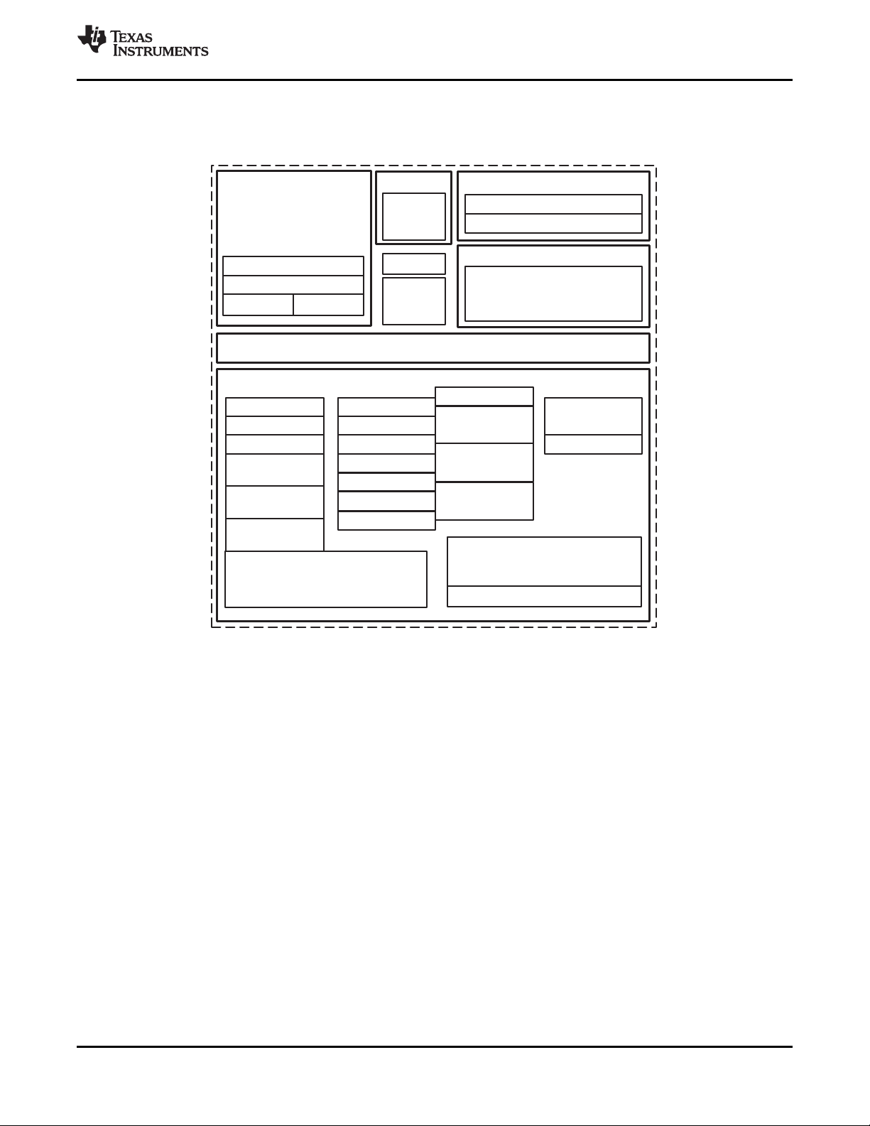
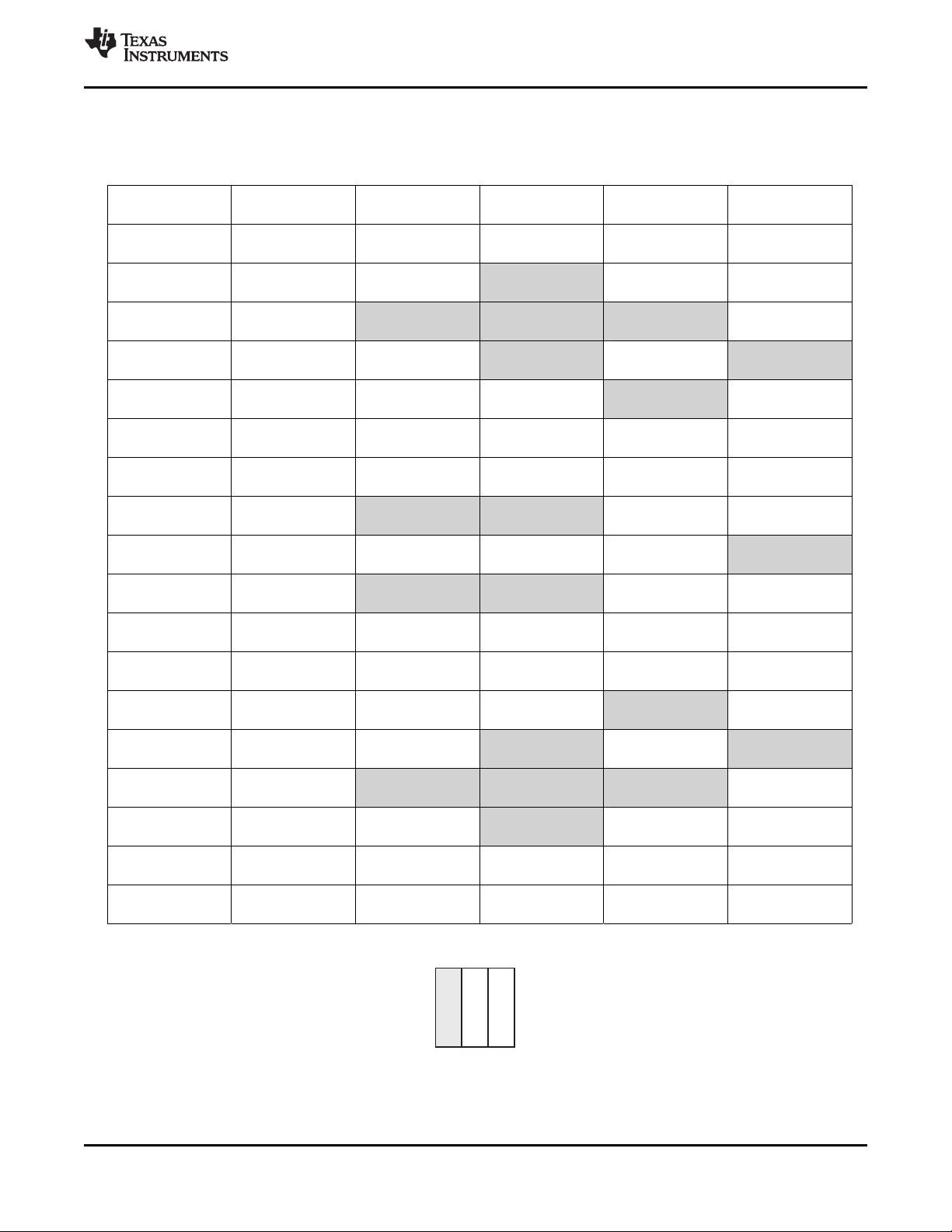
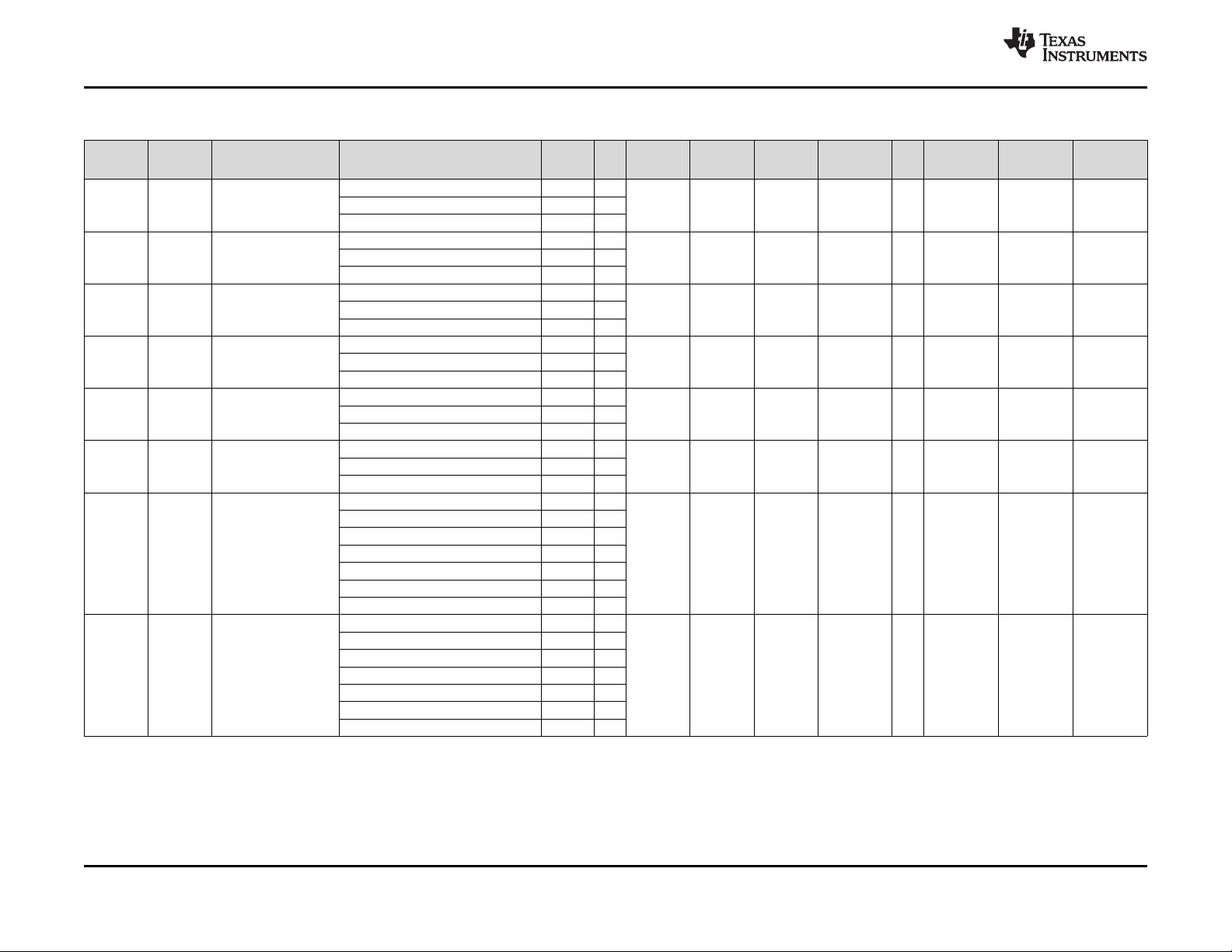
The AM335x microprocessors, based on the ARM Cortex-A8 processor, are enhanced with image,
graphics processing, peripherals and industrial interface options such as EtherCAT and PROFIBUS. The
devices support high-level operating systems (HLOS). Linux®and Android™ are available free of charge
from TI.
The AM335x microprocessor contain the subsystems shown in Figure 1-1 and a brief description of each
follows:
The microprocessor unit (MPU) subsystem is based on the ARM Cortex-A8 processor and the PowerVR
SGX™ Graphics Accelerator subsystem provides 3D graphics acceleration to support display and gaming
effects.
The PRU-ICSS is separate from the ARM core, allowing independent operation and clocking for greater
efficiency and flexibility. The PRU-ICSS enables additional peripheral interfaces and real-time protocols
such as EtherCAT, PROFINET, EtherNet/IP, PROFIBUS, Ethernet Powerlink, Sercos, and others.
Additionally, the programmable nature of the PRU-ICSS, along with its access to pins, events and all
system-on-chip (SoC) resources, provides flexibility in implementing fast, real-time responses, specialized
data handling operations, custom peripheral interfaces, and in offloading tasks from the other processor
cores of SoC.
www.ti.com
Device Information
PART NUMBER PACKAGE BODY SIZE
AM3359ZCZ NFBGA (324) 15.0 mm × 15.0 mm
AM3358ZCZ NFBGA (324) 15.0 mm × 15.0 mm
AM3357ZCZ NFBGA (324) 15.0 mm × 15.0 mm
AM3356ZCZ, AM3356ZCE NFBGA (324), NFBGA (298) 15.0 mm × 15.0 mm, 13.0 mm × 13.0 mm
AM3354ZCZ, AM3354ZCE NFBGA (324), NFBGA (298) 15.0 mm × 15.0 mm, 13.0 mm × 13.0 mm
AM3352ZCZ, AM3352ZCE NFBGA (324), NFBGA (298) 15.0 mm × 15.0 mm, 13.0 mm × 13.0 mm
AM3351ZCE NFBGA (298) 13.0 mm × 13.0 mm
(1) For more information, see Section 9, Mechanical, Packaging, and Orderable Information.
(1)
4
Device Overview Copyright © 2011–2016, Texas Instruments Incorporated
Submit Documentation Feedback
Product Folder Links: AM3359 AM3358 AM3357 AM3356 AM3354 AM3352 AM3351
Page 5
ARM
Cortex-A8
Up to 1 GHz
32KB and 32KB L1 + SED
256KB L2 + ECC
176KB ROM
64KB RAM
Graphics
PowerVR
SGX
3D GFX
Crypto
64KB
shared
RAM
24-bit LCD controller
Touch screen controller
Display
PRU-ICSS
EtherCAT, PROFINET,
EtherNet/IP,
and more
L3 and L4 interconnect
USB 2.0 HS
OTG + PHY x2
CAN x2
(Ver. 2 A and B)
McASP x2
(4 channel)
I C x3
2
SPI x2
UART x6
Serial System Parallel
eDMA
Timers x8
WDT
RTC
eHRPWM x3
eQEP x3
PRCM
eCAP x3
ADC (8 channel)
12-bit SAR
JTAG
Crystal
Oscillator x2
MMC, SD and
SDIO x3
GPIO
EMAC (2-port) 10M, 100M, 1G
IEEE 1588v2, and switch
(MII, RMII, RGMII)
mDDR(LPDDR), DDR2,
DDR3, DDR3L
(16-bit; 200, 266, 400, 400 MHz)
NAND and NOR (16-bit ECC)
Memory interface
Copyright © 2016, Texas Instruments Incorporated
www.ti.com
1.4 Functional Block Diagram
Figure 1-1 shows the AM335x microprocessor functional block diagram.
AM3359, AM3358, AM3357, AM3356, AM3354, AM3352, AM3351
SPRS717J –OCTOBER 2011–REVISED APRIL 2016
Product Folder Links: AM3359 AM3358 AM3357 AM3356 AM3354 AM3352 AM3351
Figure 1-1. AM335x Functional Block Diagram
Submit Documentation Feedback
Device OverviewCopyright © 2011–2016, Texas Instruments Incorporated
5
Page 6
AM3359, AM3358, AM3357, AM3356, AM3354, AM3352, AM3351
SPRS717J –OCTOBER 2011–REVISED APRIL 2016
Table of Contents
www.ti.com
1 Device Overview ......................................... 1
1.1 Features .............................................. 1
1.2 Applications........................................... 4
1.3 Description............................................ 4
1.4 Functional Block Diagram ........................... 5
2 Revision History ......................................... 7
3 Device Comparison ..................................... 8
3.1 Related Products ..................................... 9
4 Terminal Configuration and Functions ............ 10
4.1 Pin Diagrams........................................ 10
4.2 Pin Attributes ........................................ 18
4.3 Signal Descriptions.................................. 51
5 Specifications........................................... 80
5.1 Absolute Maximum Ratings......................... 80
5.2 ESD Ratings ........................................ 81
5.3 Power-On Hours (POH)............................. 82
5.4 Operating Performance Points (OPPs) ............. 82
5.5 Recommended Operating Conditions............... 85
5.6 Power Consumption Summary...................... 87
5.7 DC Electrical Characteristics........................ 89
5.8 Thermal Resistance Characteristics for ZCE and
ZCZ Packages ...................................... 93
5.9 External Capacitors ................................. 94
5.10 Touch Screen Controller and Analog-to-Digital
Subsystem Electrical Parameters................... 97
6 Power and Clocking ................................... 99
6.1 Power Supplies...................................... 99
6.2 Clock Specifications................................ 107
7 Peripheral Information and Timings .............. 116
7.1 Parameter Information ............................. 116
7.2 Recommended Clock and Control Signal Transition
Behavior............................................ 116
7.3 OPP50 Support .................................... 116
7.4 Controller Area Network (CAN).................... 117
7.5 DMTimer ........................................... 118
7.6 Ethernet Media Access Controller (EMAC) and
Switch.............................................. 119
7.7 External Memory Interfaces........................ 127
2
7.8 I
C.................................................. 191
7.9 JTAG Electrical Data and Timing.................. 193
7.10 LCD Controller (LCDC) ............................ 194
7.11 Multichannel Audio Serial Port (McASP) .......... 210
7.12 Multichannel Serial Port Interface (McSPI) ........ 215
7.13 Multimedia Card (MMC) Interface ................. 221
7.14 Programmable Real-Time Unit Subsystem and
Industrial Communication Subsystem (PRU-ICSS) 224
7.15 Universal Asynchronous Receiver Transmitter
(UART)............................................. 233
8 Device and Documentation Support.............. 236
8.1 Device Nomenclature .............................. 236
8.2 Tools and Software ................................ 237
8.3 Documentation Support............................ 241
8.4 Related Links ...................................... 244
8.5 Community Resources............................. 244
8.6 Trademarks ........................................ 244
8.7 Electrostatic Discharge Caution ................... 244
8.8 Glossary............................................ 244
9 Mechanical, Packaging, and Orderable
Information............................................. 245
9.1 Via Channel........................................ 245
9.2 Packaging Information ............................. 245
6
Table of Contents Copyright © 2011–2016, Texas Instruments Incorporated
Submit Documentation Feedback
Product Folder Links: AM3359 AM3358 AM3357 AM3356 AM3354 AM3352 AM3351
Page 7

AM3359, AM3358, AM3357, AM3356, AM3354, AM3352, AM3351
www.ti.com
SPRS717J –OCTOBER 2011–REVISED APRIL 2016
2 Revision History
NOTE: Page numbers for previous revisions may differ from page numbers in the current version.
Changes from Revision I (December 2015) to Revision J Page
• Added Secure boot to Security feature list ........................................................................................ 3
• Added extended temperature range for the AM3351 device in Table 3-1 .................................................... 8
• Added Section 3.1, Related Products ............................................................................................. 9
• Reformatted and added content to Section 8, Device and Documentation Support...................................... 236
Submit Documentation Feedback
Product Folder Links: AM3359 AM3358 AM3357 AM3356 AM3354 AM3352 AM3351
Revision HistoryCopyright © 2011–2016, Texas Instruments Incorporated
7
Page 8
AM3359, AM3358, AM3357, AM3356, AM3354, AM3352, AM3351
SPRS717J –OCTOBER 2011–REVISED APRIL 2016
www.ti.com
3 Device Comparison
Table 3-1 shows the features supported across different AM335x devices.
Table 3-1. Device Features Comparison
FUNCTION AM3351 AM3352 AM3354 AM3356 AM3357 AM3358 AM3359
ARM Cortex-A8 Yes Yes Yes Yes Yes Yes Yes
Frequency
MIPS
On-chip L1 cache 64KB 64KB 64KB 64KB 64KB 64KB 64KB
On-chip L2 cache 256KB 256KB 256KB 256KB 256KB 256KB 256KB
Graphics accelerator
(SGX530)
Hardware acceleration Crypto
Programmable real-time
unit subsystem and
industrial communication
subsystem (PRU-ICSS)
On-chip memory 128KB 128KB 128KB 128KB 128KB 128KB 128KB
Display options LCD LCD LCD LCD LCD LCD LCD
General-purpose memory 1 16-bit (GPMC,
DRAM
Universal serial bus (USB) ZCE: 1 port ZCE: 1 port
Ethernet media access
controller (EMAC) with 2port switch
Multimedia card (MMC) 3 3 3 3 3 3 3
Controller-area network
(CAN)
Universal asynchronous
receiver and transmitter
(UART)
Analog-to-digital converter
(ADC)
Enhanced high-resolution
PWM modules
(eHRPWM)
Enhanced capture
modules (eCAP)
Enhanced quadrature
encoder pulse (eQEP)
Real-time clock (RTC) 1 1 1 1 1 1 1
Inter-integrated circuit
(I2C)
(1)
(2)
(3)
300 MHz
600 MHz
600
1200
— — 3D — — 3D 3D
accelerator
— — — Features
NAND flash,
NOR flash,
SRAM)
1 16-bit
(LPDDR-400,
DDR2-532,
DDR3-800)
10/100/1000
ZCE: 1 port
— 2 2 2 2 2 2
6 6 6 6 6 6 6
8-ch 12-bit 8-ch 12-bit 8-ch 12-bit 8-ch 12-bit 8-ch 12-bit 8-ch 12-bit 8-ch 12-bit
3 3 3 3 3 3 3
3 3 3 3 3 3 3
3 3 3 3 3 3 3
3 3 3 3 3 3 3
300 MHz
600 MHz
800 MHz
1000 MHz
600
1200
1600
2000
Crypto
accelerator
1 16-bit (GPMC,
NAND flash,
NOR flash,
SRAM)
1 16-bit
(LPDDR-400,
DDR2-532,
DDR3-800)
ZCZ: 2 ports
10/100/1000
ZCE: 1 port
ZCZ: 2 ports
600 MHz
800 MHz
1000 MHz
1200
1600
2000
Crypto
accelerator
1 16-bit (GPMC,
NAND flash,
NOR flash,
SRAM)
1 16-bit
(LPDDR-400,
DDR2-532,
DDR3-800)
ZCE: 1 port
ZCZ: 2 ports
10/100/1000
ZCE: 1 port
ZCZ: 2 ports
300 MHz
600 MHz
800 MHz
600
1200
1600
Crypto
accelerator
including basic
Industrial
protocols;
ZCE: Limited
PRU I/Os pinned
out
1 16-bit (GPMC,
NAND flash,
NOR flash,
SRAM)
1 16-bit
(LPDDR-400,
DDR2-532,
DDR3-800)
ZCE: 1 port
ZCZ: 2 ports
10/100/1000
ZCE: 1 port
ZCZ: 2 ports
300 MHz
600 MHz
800 MHz
600
1200
1600
Crypto
accelerator
Features
including all
Industrial
protocols
1 16-bit (GPMC,
NAND flash,
NOR flash,
SRAM)
1 16-bit
(LPDDR-400,
DDR2-532,
DDR3-800)
No ZCE
Available
ZCZ: 2 ports
10/100/1000
No ZCE
Available
ZCZ: 2 ports
600 MHz
800 MHz
1000 MHz
1200
1600
2000
Crypto
accelerator
Features
including basic
Industrial
protocols
1 16-bit (GPMC,
NAND flash,
NOR flash,
SRAM)
1 16-bit
(LPDDR-400,
DDR2-532,
DDR3-800)
No ZCE
Available
ZCZ: 2 ports
10/100/1000
No ZCE
Available
ZCZ: 2 ports
600 MHz
800 MHz
1200
1600
Crypto
accelerator
Features
including all
Industrial
protocols
1 16-bit (GPMC,
NAND flash,
NOR flash,
SRAM)
1 16-bit
(LPDDR-400,
DDR2-532,
DDR3-800)
No ZCE
Available
ZCZ: 2 ports
10/100/1000
No ZCE
Available
ZCZ: 2 ports
8
Device Comparison Copyright © 2011–2016, Texas Instruments Incorporated
Submit Documentation Feedback
Product Folder Links: AM3359 AM3358 AM3357 AM3356 AM3354 AM3352 AM3351
Page 9
AM3359, AM3358, AM3357, AM3356, AM3354, AM3352, AM3351
www.ti.com
SPRS717J –OCTOBER 2011–REVISED APRIL 2016
Table 3-1. Device Features Comparison (continued)
FUNCTION AM3351 AM3352 AM3354 AM3356 AM3357 AM3358 AM3359
Multichannel audio serial
port (McASP)
Multichannel serial port
interface (McSPI)
Enhanced direct memory
access (EDMA)
Input/output (I/O) supply 1.8 V, 3.3 V 1.8 V, 3.3 V 1.8 V, 3.3 V 1.8 V, 3.3 V 1.8 V, 3.3 V 1.8 V, 3.3 V 1.8 V, 3.3 V
Operating temperature
range
(1) Frequencies listed correspond to silicon revision 2.x. Earlier silicon revisions support 275 MHz, 500 MHz, 600 MHz, and 720 MHz.
(2) MIPS listed correspond to silicon revision 2.x. Earlier silicon revisions support 560, 1000, 1200, and 1440.
(3) DRAM speeds listed are data rates.
(4) Industrial extended temperature only supported for 300-MHz and 600-MHz frequencies.
2 2 2 2 2 2 2
2 2 2 2 2 2 2
64-Ch 64-Ch 64-Ch 64-Ch 64-Ch 64-Ch 64-Ch
0 to 90°C
–40 to 105°C
-40 to 125°C
–40 to 105°C
–40 to 90°C
0 to 90°C
(4)
–40 to 105°C
–40 to 90°C
0 to 90°C
–40 to 105°C
–40 to 90°C
0 to 90°C
–40 to 105°C
–40 to 90°C
–40 to 105°C
–40 to 90°C
0 to 90°C
–40 to 105°C
–40 to 90°C
3.1 Related Products
For information about other devices in this family of products, see the following links:
Sitara Processors Scalable processors based on ARM Cortex-A cores with flexible peripherals,
connectivity and unified software support – perfect for sensors to servers.
TI's ARM Cortex-A8 Advantage The ARM Cortex-A8 core is highly-optimized by ARM for performance
and power efficiency. With the ability to scale in speed from 300MHz to 1.35GHz, the ARM
Cortex-A8-based processor can meet the requirements for power optimized devices with a
power budget of less than the Cortex-A8 core a dual-issue superscalar, achieving twice the
instructions executed per clock cycle at 2 DMIPS/MHz.
Sitara AM335x Processors Scalable ARM Cortex-A8-based core from 300 MHz up to 1 GHz, 3D
graphics option for enhanced user interface, dual-core PRU-ICSS for industrial Ethernet
protocols and position feedback control, and premium secure boot option.
Companion Products for Sitara AM335x Processors Review products that are frequently purchased or
used in conjunction with this product.
TI Designs for Sitara AM335x Processors TI Designs Reference Design Library is a robust reference
design library spanning analog, embedded processor and connectivity. Created by TI experts
to help you jump start your system design, all TI Designs include schematic or block
diagrams, BOMs and design files to speed your time to market. Search and download
designs at ti.com/tidesigns.
Submit Documentation Feedback
Product Folder Links: AM3359 AM3358 AM3357 AM3356 AM3354 AM3352 AM3351
Device ComparisonCopyright © 2011–2016, Texas Instruments Incorporated
9
Page 10

AM3359, AM3358, AM3357, AM3356, AM3354, AM3352, AM3351
SPRS717J –OCTOBER 2011–REVISED APRIL 2016
4 Terminal Configuration and Functions
4.1 Pin Diagrams
NOTE
The terms 'ball', 'pin', and 'terminal' are used interchangeably throughout the document. An
attempt is made to use 'ball' only when referring to the physical package.
4.1.1 ZCE Package Pin Maps (Top View)
The pin maps that follow show the pin assignments on the ZCE package in three sections (left, middle,
and right).
www.ti.com
10
Terminal Configuration and Functions Copyright © 2011–2016, Texas Instruments Incorporated
Submit Documentation Feedback
Product Folder Links: AM3359 AM3358 AM3357 AM3356 AM3354 AM3352 AM3351
Page 11
Left
Pin map section location
AM3359, AM3358, AM3357, AM3356, AM3354, AM3352, AM3351
www.ti.com
SPRS717J –OCTOBER 2011–REVISED APRIL 2016
ZCE Pin Map [Section Left - Top View]
A B C D E F
19 VSS I2C0_SCL UART1_TXD UART1_RTSn UART0_RXD UART0_CTSn
18 SPI0_SCLK SPI0_D0 I2C0_SDA UART1_RXD ECAP0_IN_PWM0_OUT UART0_RTSn
17 SPI0_CS0 SPI0_D1 EXTINTn XXXX UART1_CTSn UART0_TXD
16 WARMRSTn SPI0_CS1 XXXX XXXX XXXX VDDS
15 EMU0 XDMA_EVENT_INTR1 XDMA_EVENT_INTR0 XXXX PWRONRSTn XXXX
14 TDO TCK TMS EMU1 XXXX VDDSHV6
13 TRSTn TDI CAP_VBB_MPU CAP_VDD_SRAM_MPU VDDSHV6 VSS
12 AIN7 AIN5 VDDS_SRAM_MPU_BB VDDS VDDSHV6 VSS
11 AIN1 AIN3 XXXX XXXX VDDSHV6 VDD_CORE
10 AIN6 CAP_VDD_SRAM_CORE VDDS_SRAM_CORE_BG VSS VSS XXXX
9 VREFP VREFN XXXX XXXX VSS VDD_CORE
8 AIN2 AIN0 AIN4 VSSA_ADC VSS VSS
7 RTC_KALDO_ENn RTC_PWRONRSTn PMIC_POWER_EN VDDA_ADC VSS VSS
6 RTC_XTALIN RESERVED VDDS_RTC CAP_VDD_RTC XXXX VSS
5 RTC_XTALOUT EXT_WAKEUP VDDS_PLL_DDR XXXX DDR_A4 XXXX
4 DDR_WEn DDR_BA2 XXXX XXXX XXXX DDR_A12
3 DDR_BA0 DDR_A3 DDR_A8 XXXX DDR_A15 DDR_A0
2 DDR_A5 DDR_A9 DDR_CK DDR_A7 DDR_A10 DDR_RASn
1 VSS DDR_A6 DDR_CKn DDR_A2 DDR_BA1 DDR_CASn
Terminal Configuration and FunctionsCopyright © 2011–2016, Texas Instruments Incorporated
Submit Documentation Feedback
Product Folder Links: AM3359 AM3358 AM3357 AM3356 AM3354 AM3352 AM3351
11
Page 12
Middle
Pin map section location
AM3359, AM3358, AM3357, AM3356, AM3354, AM3352, AM3351
SPRS717J –OCTOBER 2011–REVISED APRIL 2016
ZCE Pin Map [Section Middle - Top View]
G H J K L M
19 MMC0_CLK MMC0_DAT3 MII1_COL MII1_RX_ER MII1_RX_DV MII1_RX_CLK
18 MMC0_DAT0 MMC0_DAT2 MII1_CRS RMII1_REF_CLK MII1_TXD0 MII1_TXD1
17 MMC0_CMD MMC0_DAT1 XXXX MII1_TX_EN XXXX MII1_TXD3
16 USB0_DRVVBUS VDDS_PLL_MPU XXXX VDD_CORE XXXX VDDS
15 VDDSHV4 VDDSHV4 VSS VDD_CORE VSS VDDSHV5
14 XXXX VDDSHV4 VSS XXXX VSS VDDSHV5
13 XXXX VDD_CORE VDD_CORE XXXX VDD_CORE VDD_CORE
12 VSS VDD_CORE VDD_CORE VSS VDD_CORE VDD_CORE
www.ti.com
11 VDD_CORE VSS VSS VSS VSS VSS
10 XXXX VSS XXXX XXXX XXXX VSS
9 VDD_CORE VSS VSS VSS VSS VSS
8 VSS VDD_CORE VDD_CORE VSS VDD_CORE VDD_CORE
7 XXXX VDD_CORE VDD_CORE XXXX VDD_CORE VDD_CORE
6 XXXX VDDS_DDR VSS XXXX VSS VDDS_DDR
5 VDDS_DDR VDDS_DDR VSS VDDS_DDR VSS VDDS_DDR
4 DDR_A11 DDR_VREF XXXX VDDS_DDR XXXX DDR_D11
3 DDR_CKE DDR_A14 XXXX DDR_DQM1 XXXX DDR_D10
2 DDR_RESETn DDR_CSn0 DDR_A1 DDR_D8 DDR_DQSn1 DDR_D12
1 DDR_ODT DDR_A13 DDR_VTP DDR_D9 DDR_DQS1 DDR_D13
12
Terminal Configuration and Functions Copyright © 2011–2016, Texas Instruments Incorporated
Submit Documentation Feedback
Product Folder Links: AM3359 AM3358 AM3357 AM3356 AM3354 AM3352 AM3351
Page 13
Right
Pin map section location
AM3359, AM3358, AM3357, AM3356, AM3354, AM3352, AM3351
www.ti.com
SPRS717J –OCTOBER 2011–REVISED APRIL 2016
ZCE Pin Map [Section Right - Top View]
N P R T U V W
19 MII1_TX_CLK MII1_RXD1 MDC USB0_VBUS USB0_DP USB0_ID VSS
18 MII1_TXD2 MII1_RXD0 VDDA3P3V_USB0 USB0_CE USB0_DM GPMC_BEn1 GPMC_WPn
17 MII1_RXD3 MDIO VDDA1P8V_USB0 XXXX GPMC_CSn3 GPMC_AD15 GPMC_AD14
16 MII1_RXD2 VSSA_USB XXXX XXXX XXXX GPMC_CLK GPMC_AD9
15 VDDSHV5 XXXX GPMC_WAIT0 XXXX GPMC_CSn2 GPMC_AD8 GPMC_AD7
14 XXXX VSS XXXX VDDS GPMC_AD6 GPMC_CSn1 GPMC_AD5
13 XXXX VSS VDDSHV1 GPMC_AD13 GPMC_AD12 GPMC_AD4 GPMC_AD3
12 VSS VSS VDDSHV1 GPMC_AD10 GPMC_AD11 GPMC_AD2 XTALOUT
11 VDD_CORE VDD_CORE VDDSHV1 XXXX XXXX VSS_OSC XTALIN
10 XXXX XXXX VSS VSS VDDS_OSC GPMC_ADVn_ALE GPMC_AD0
9 VDD_CORE VDD_CORE VDDSHV1 XXXX XXXX GPMC_AD1 GPMC_OEn_REn
8 VSS VSS VDDSHV1 VDDS_PLL_CORE_LCD GPMC_WEn GPMC_BEn0_CLE GPMC_CSn0
7 XXXX VSS VDDSHV6 LCD_HSYNC LCD_VSYNC LCD_DATA15 LCD_AC_BIAS_EN
6 XXXX VDDSHV6 XXXX VDDS LCD_DATA13 LCD_DATA12 LCD_DATA14
5 VDDS_DDR XXXX VPP XXXX LCD_DATA10 LCD_DATA11 LCD_PCLK
4 DDR_D0 DDR_D1 XXXX XXXX XXXX LCD_DATA8 LCD_DATA9
3 DDR_DQM0 DDR_D4 DDR_D7 XXXX LCD_DATA7 LCD_DATA6 LCD_DATA5
2 DDR_D14 DDR_D2 DDR_DQSn0 DDR_D6 LCD_DATA1 LCD_DATA3 LCD_DATA4
1 DDR_D15 DDR_D3 DDR_DQS0 DDR_D5 LCD_DATA0 LCD_DATA2 VSS
Terminal Configuration and FunctionsCopyright © 2011–2016, Texas Instruments Incorporated
Submit Documentation Feedback
Product Folder Links: AM3359 AM3358 AM3357 AM3356 AM3354 AM3352 AM3351
13
Page 14

AM3359, AM3358, AM3357, AM3356, AM3354, AM3352, AM3351
SPRS717J –OCTOBER 2011–REVISED APRIL 2016
4.1.2 ZCZ Package Pin Maps (Top View)
The pin maps that follow show the pin assignments on the ZCZ package in three sections (left, middle,
and right).
www.ti.com
14
Terminal Configuration and Functions Copyright © 2011–2016, Texas Instruments Incorporated
Submit Documentation Feedback
Product Folder Links: AM3359 AM3358 AM3357 AM3356 AM3354 AM3352 AM3351
Page 15
Left
Pin map section location
AM3359, AM3358, AM3357, AM3356, AM3354, AM3352, AM3351
www.ti.com
SPRS717J –OCTOBER 2011–REVISED APRIL 2016
ZCZ Pin Map [Section Left - Top View]
A B C D E F
18 VSS EXTINTn ECAP0_IN_PWM0_OUT UART1_CTSn UART0_CTSn MMC0_DAT2
17 SPI0_SCLK SPI0_D0 I2C0_SDA UART1_RTSn UART0_RTSn MMC0_DAT3
16 SPI0_CS0 SPI0_D1 I2C0_SCL UART1_RXD UART0_TXD USB0_DRVVBUS
15 XDMA_EVENT_INTR0 PWRONRSTn SPI0_CS1 UART1_TXD UART0_RXD USB1_DRVVBUS
14 MCASP0_AHCLKX EMU1 EMU0 XDMA_EVENT_INTR1 VDDS VDDSHV6
13 MCASP0_ACLKX MCASP0_FSX MCASP0_FSR MCASP0_AXR1 VDDSHV6 VDD_MPU
12 TCK MCASP0_ACLKR MCASP0_AHCLKR MCASP0_AXR0 VDDSHV6 VDD_MPU
11 TDO TDI TMS CAP_VDD_SRAM_MPU VDDSHV6 VDD_MPU
10 WARMRSTn TRSTn CAP_VBB_MPU VDDS_SRAM_MPU_BB VDDSHV6 VDD_MPU
9 VREFN VREFP AIN7 CAP_VDD_SRAM_CORE VDDS_SRAM_CORE_BG VDDS
8 AIN6 AIN5 AIN4 VDDA_ADC VSSA_ADC VSS
7 AIN3 AIN2 AIN1 VDDS_RTC VDDS_PLL_DDR VDD_CORE
6 RTC_XTALIN AIN0 PMIC_POWER_EN CAP_VDD_RTC VDDS VDD_CORE
5 VSS_RTC RTC_PWRONRSTn EXT_WAKEUP DDR_A6 VDDS_DDR VDDS_DDR
4 RTC_XTALOUT RTC_KALDO_ENn DDR_BA0 DDR_A8 DDR_A2 DDR_A10
3 RESERVED DDR_BA2 DDR_A3 DDR_A15 DDR_A12 DDR_A0
2 VDD_MPU_MON DDR_WEn DDR_A4 DDR_CK DDR_A7 DDR_A11
1 VSS DDR_A5 DDR_A9 DDR_CKn DDR_BA1 DDR_CASn
Terminal Configuration and FunctionsCopyright © 2011–2016, Texas Instruments Incorporated
Submit Documentation Feedback
Product Folder Links: AM3359 AM3358 AM3357 AM3356 AM3354 AM3352 AM3351
15
Page 16
Middle
Pin map section location
AM3359, AM3358, AM3357, AM3356, AM3354, AM3352, AM3351
SPRS717J –OCTOBER 2011–REVISED APRIL 2016
ZCZ Pin Map [Section Middle - Top View]
G H J K L M
18 MMC0_CMD RMII1_REF_CLK MII1_TXD3 MII1_TX_CLK MII1_RX_CLK MDC
17 MMC0_CLK MII1_CRS MII1_RX_DV MII1_TXD0 MII1_RXD3 MDIO
16 MMC0_DAT0 MII1_COL MII1_TX_EN MII1_TXD1 MII1_RXD2 MII1_RXD0
15 MMC0_DAT1 VDDS_PLL_MPU MII1_RX_ER MII1_TXD2 MII1_RXD1 USB0_CE
14 VDDSHV6 VDDSHV4 VDDSHV4 VDDSHV5 VDDSHV5 VSSA_USB
13 VDD_MPU VDD_MPU VDD_MPU VDDS VSS VDD_CORE
12 VSS VSS VDD_CORE VDD_CORE VSS VSS
11 VSS VDD_CORE VSS VSS VSS VDD_CORE
www.ti.com
10 VDD_CORE VSS VSS VSS VSS VSS
9 VSS VSS VSS VSS VDD_CORE VSS
8 VSS VSS VSS VDD_CORE VDD_CORE VSS
7 VDD_CORE VSS VSS VSS VDD_CORE VSS
6 VDD_CORE VSS VSS VDD_CORE VDD_CORE VSS
5 VDDS_DDR VDDS_DDR VDDS_DDR VDDS_DDR VDDS_DDR VPP
4 DDR_RASn DDR_A14 DDR_VREF DDR_D12 DDR_D14 DDR_D1
3 DDR_CKE DDR_A13 DDR_VTP DDR_D11 DDR_D13 DDR_D0
2 DDR_RESETn DDR_CSn0 DDR_DQM1 DDR_D10 DDR_DQSn1 DDR_DQM0
1 DDR_ODT DDR_A1 DDR_D8 DDR_D9 DDR_DQS1 DDR_D15
16
Terminal Configuration and Functions Copyright © 2011–2016, Texas Instruments Incorporated
Submit Documentation Feedback
Product Folder Links: AM3359 AM3358 AM3357 AM3356 AM3354 AM3352 AM3351
Page 17

Right
Pin map section location
AM3359, AM3358, AM3357, AM3356, AM3354, AM3352, AM3351
www.ti.com
SPRS717J –OCTOBER 2011–REVISED APRIL 2016
ZCZ Pin Map [Section Right - Top View]
N P R T U V
18 USB0_DM USB1_CE USB1_DM USB1_VBUS GPMC_BEn1 VSS
17 USB0_DP USB1_ID USB1_DP GPMC_WAIT0 GPMC_WPn GPMC_A11
16 VDDA1P8V_USB0 USB0_ID VDDA1P8V_USB1 GPMC_A10 GPMC_A9 GPMC_A8
15 VDDA3P3V_USB0 USB0_VBUS VDDA3P3V_USB1 GPMC_A7 GPMC_A6 GPMC_A5
14 VSSA_USB VDDS GPMC_A4 GPMC_A3 GPMC_A2 GPMC_A1
13 VDD_CORE VDDSHV3 GPMC_A0 GPMC_CSn3 GPMC_AD15 GPMC_AD14
12 VDD_CORE VDDSHV3 GPMC_AD13 GPMC_AD12 GPMC_AD11 GPMC_CLK
11 VSS VDDSHV2 VDDS_OSC GPMC_AD10 XTALOUT VSS_OSC
10 VSS VDDSHV2 VDDS_PLL_CORE_LCD GPMC_AD9 GPMC_AD8 XTALIN
9 VDD_CORE VDDS GPMC_AD6 GPMC_AD7 GPMC_CSn1 GPMC_CSn2
8 VDD_CORE VDDSHV1 GPMC_AD2 GPMC_AD3 GPMC_AD4 GPMC_AD5
7 VSS VDDSHV1 GPMC_ADVn_ALE GPMC_OEn_REn GPMC_AD0 GPMC_AD1
6 VDDS VDDSHV6 LCD_AC_BIAS_EN GPMC_BEn0_CLE GPMC_WEn GPMC_CSn0
5 VDDSHV6 VDDSHV6 LCD_HSYNC LCD_DATA15 LCD_VSYNC LCD_PCLK
4 DDR_D5 DDR_D7 LCD_DATA3 LCD_DATA7 LCD_DATA11 LCD_DATA14
3 DDR_D4 DDR_D6 LCD_DATA2 LCD_DATA6 LCD_DATA10 LCD_DATA13
2 DDR_D3 DDR_DQSn0 LCD_DATA1 LCD_DATA5 LCD_DATA9 LCD_DATA12
1 DDR_D2 DDR_DQS0 LCD_DATA0 LCD_DATA4 LCD_DATA8 VSS
Terminal Configuration and FunctionsCopyright © 2011–2016, Texas Instruments Incorporated
Submit Documentation Feedback
Product Folder Links: AM3359 AM3358 AM3357 AM3356 AM3354 AM3352 AM3351
17
Page 18

AM3359, AM3358, AM3357, AM3356, AM3354, AM3352, AM3351
SPRS717J –OCTOBER 2011–REVISED APRIL 2016
4.2 Pin Attributes
The AM335x Sitara Processors Technical Reference Manual (SPRUH73) and this document may
reference internal signal names when discussing peripheral input and output signals because many of the
AM335x package terminals can be multiplexed to one of several peripheral signals. The following table
has a Pin Name column that lists all device terminal names and a Signal Name column that lists all
internal signal names multiplexed to each terminal which provides a cross reference of internal signal
names to terminal names. This table also identifies other important terminal characteristics.
1. BALL NUMBER: Package ball numbers associated with each signals.
2. PIN NAME: The name of the package pin or terminal.
Note: The table does not take into account subsystem terminal multiplexing options.
3. SIGNAL NAME: The signal name for that pin in the mode being used.
4. MODE: Multiplexing mode number.
(a) Mode 0 is the primary mode; this means that when mode 0 is set, the function mapped on the
terminal corresponds to the name of the terminal. There is always a function mapped on the
primary mode. Notice that primary mode is not necessarily the default mode.
Note: The default mode is the mode at the release of the reset; also see the RESET REL. MODE
column.
(b) Modes 1 to 7 are possible modes for alternate functions. On each terminal, some modes are
effectively used for alternate functions, while some modes are not used and do not correspond to a
functional configuration.
5. TYPE: Signal direction
– I = Input
– O = Output
– I/O = Input and Output
– D = Open drain
– DS = Differential
– A = Analog
– PWR = Power
– GND = Ground
Note: In the safe_mode, the buffer is configured in high-impedance.
6. BALL RESET STATE: State of the terminal while the active low PWRONRSTn terminal is low.
– 0: The buffer drives VOL(pulldown or pullup resistor not activated)
0(PD): The buffer drives VOLwith an active pulldown resistor
– 1: The buffer drives VOH(pulldown or pullup resistor not activated)
1(PU): The buffer drives VOHwith an active pullup resistor
– Z: High-impedance
– L: High-impedance with an active pulldown resistor
– H : High-impedance with an active pullup resistor
7. BALL RESET REL. STATE: State of the terminal after the active low PWRONRSTn terminal
transitions from low to high.
– 0: The buffer drives VOL(pulldown or pullup resistor not activated)
0(PD): The buffer drives VOLwith an active pulldown resistor
– 1: The buffer drives VOH(pulldown or pullup resistor not activated)
1(PU): The buffer drives VOHwith an active pullup resistor
– Z: High-impedance.
– L: High-impedance with an active pulldown resistor
– H : High-impedance with an active pullup resistor
8. RESET REL. MODE: The mode is automatically configured after the active low PWRONRSTn terminal
transitions from low to high.
9. POWER: The voltage supply that powers the terminal’s IO buffers.
www.ti.com
18
Terminal Configuration and Functions Copyright © 2011–2016, Texas Instruments Incorporated
Submit Documentation Feedback
Product Folder Links: AM3359 AM3358 AM3357 AM3356 AM3354 AM3352 AM3351
Page 19

www.ti.com
10. HYS: Indicates if the input buffer is with hysteresis.
11. BUFFER STRENGTH: Drive strength of the associated output buffer.
12. PULLUP OR PULLDOWN TYPE: Denotes the presence of an internal pullup or pulldown resistor.
13. IO CELL: IO cell information.
AM3359, AM3358, AM3357, AM3356, AM3354, AM3352, AM3351
SPRS717J –OCTOBER 2011–REVISED APRIL 2016
Pullup and pulldown resistors can be enabled or disabled via software.
Note: Configuring two terminals to the same input signal is not supported as it can yield unexpected
results. This can be easily prevented with the proper software configuration.
Terminal Configuration and FunctionsCopyright © 2011–2016, Texas Instruments Incorporated
Submit Documentation Feedback
Product Folder Links: AM3359 AM3358 AM3357 AM3356 AM3354 AM3352 AM3351
19
Page 20
AM3359, AM3358, AM3357, AM3356, AM3354, AM3352, AM3351
SPRS717J –OCTOBER 2011–REVISED APRIL 2016
Table 4-1. Pin Attributes (ZCE and ZCZ Packages)
www.ti.com
ZCE BALL
NUMBER [1]
B8 B6 AIN0 AIN0 0 A
A11 C7 AIN1 AIN1 0 A
A8 B7 AIN2 AIN2 0 A
B11 A7 AIN3 AIN3 0 A
C8 C8 AIN4 AIN4 0 A
B12 B8 AIN5 AIN5 0 A Z Z 0 VDDA_ADC /
A10 A8 AIN6 AIN6 0 A Z Z 0 VDDA_ADC /
A12 C9 AIN7 AIN7 0 A Z Z 0 VDDA_ADC /
C13 C10 CAP_VBB_MPU CAP_VBB_MPU NA A
D6 D6 CAP_VDD_RTC CAP_VDD_RTC NA A
B10 D9 CAP_VDD_SRAM_CORE CAP_VDD_SRAM_CORE NA A
D13 D11 CAP_VDD_SRAM_MPU CAP_VDD_SRAM_MPU NA A
F3 F3 DDR_A0 ddr_a0 0 O H 1 0 VDDS_DDR /
J2 H1 DDR_A1 ddr_a1 0 O H 1 0 VDDS_DDR /
D1 E4 DDR_A2 ddr_a2 0 O H 1 0 VDDS_DDR /
B3 C3 DDR_A3 ddr_a3 0 O H 1 0 VDDS_DDR /
E5 C2 DDR_A4 ddr_a4 0 O H 1 0 VDDS_DDR /
A2 B1 DDR_A5 ddr_a5 0 O H 1 0 VDDS_DDR /
B1 D5 DDR_A6 ddr_a6 0 O H 1 0 VDDS_DDR /
D2 E2 DDR_A7 ddr_a7 0 O H 1 0 VDDS_DDR /
C3 D4 DDR_A8 ddr_a8 0 O H 1 0 VDDS_DDR /
B2 C1 DDR_A9 ddr_a9 0 O H 1 0 VDDS_DDR /
E2 F4 DDR_A10 ddr_a10 0 O H 1 0 VDDS_DDR /
G4 F2 DDR_A11 ddr_a11 0 O H 1 0 VDDS_DDR /
ZCZ BALL
NUMBER [1]
PIN NAME [2] SIGNAL NAME [3] MODE [4]
TYPE
BALL RESET
[5]
STATE [6]
(22)
Z Z 0 VDDA_ADC /
(21)
Z Z 0 VDDA_ADC /
(21)
Z Z 0 VDDA_ADC /
(20)
Z Z 0 VDDA_ADC /
(20)
Z Z 0 VDDA_ADC /
BALL RESET
REL. STATE
(25)
[7]
RESET REL.
MODE [8]
ZCE POWER /
ZCZ POWER [9]
VDDA_ADC
VDDA_ADC
VDDA_ADC
VDDA_ADC
VDDA_ADC
VDDA_ADC
VDDA_ADC
VDDA_ADC
VDDS_DDR
VDDS_DDR
VDDS_DDR
VDDS_DDR
VDDS_DDR
VDDS_DDR
VDDS_DDR
VDDS_DDR
VDDS_DDR
VDDS_DDR
VDDS_DDR
VDDS_DDR
BUFFER
HYS
STRENGTH
[10]
(mA) [11]
NA 25 NA Analog
NA 25 NA Analog
NA 25 NA Analog
NA 25 NA Analog
NA 25 NA Analog
NA NA NA Analog
NA NA NA Analog
NA NA NA Analog
NA 8 PU/PD LVCMOS/SSTL/
NA 8 PU/PD LVCMOS/SSTL/
NA 8 PU/PD LVCMOS/SSTL/
NA 8 PU/PD LVCMOS/SSTL/
NA 8 PU/PD LVCMOS/SSTL/
NA 8 PU/PD LVCMOS/SSTL/
NA 8 PU/PD LVCMOS/SSTL/
NA 8 PU/PD LVCMOS/SSTL/
NA 8 PU/PD LVCMOS/SSTL/
NA 8 PU/PD LVCMOS/SSTL/
NA 8 PU/PD LVCMOS/SSTL/
NA 8 PU/PD LVCMOS/SSTL/
PULLUP
/DOWN TYPE
[12]
I/O CELL [13]
HSTL
HSTL
HSTL
HSTL
HSTL
HSTL
HSTL
HSTL
HSTL
HSTL
HSTL
HSTL
20
Copyright © 2011–2016, Texas Instruments IncorporatedTerminal Configuration and Functions
Submit Documentation Feedback
Product Folder Links: AM3359 AM3358 AM3357 AM3356 AM3354 AM3352 AM3351
Page 21

AM3359, AM3358, AM3357, AM3356, AM3354, AM3352, AM3351
www.ti.com
Table 4-1. Pin Attributes (ZCE and ZCZ Packages) (continued)
ZCE BALL
NUMBER [1]
F4 E3 DDR_A12 ddr_a12 0 O H 1 0 VDDS_DDR /
H1 H3 DDR_A13 ddr_a13 0 O H 1 0 VDDS_DDR /
H3 H4 DDR_A14 ddr_a14 0 O H 1 0 VDDS_DDR /
E3 D3 DDR_A15 ddr_a15 0 O H 1 0 VDDS_DDR /
A3 C4 DDR_BA0 ddr_ba0 0 O H 1 0 VDDS_DDR /
E1 E1 DDR_BA1 ddr_ba1 0 O H 1 0 VDDS_DDR /
B4 B3 DDR_BA2 ddr_ba2 0 O H 1 0 VDDS_DDR /
F1 F1 DDR_CASn ddr_casn 0 O H 1 0 VDDS_DDR /
C2 D2 DDR_CK ddr_ck 0 O L 0 0 VDDS_DDR /
G3 G3 DDR_CKE ddr_cke 0 O L 0 0 VDDS_DDR /
C1 D1 DDR_CKn ddr_nck 0 O H 1 0 VDDS_DDR /
H2 H2 DDR_CSn0 ddr_csn0 0 O H 1 0 VDDS_DDR /
N4 M3 DDR_D0 ddr_d0 0 I/O L Z 0 VDDS_DDR /
P4 M4 DDR_D1 ddr_d1 0 I/O L Z 0 VDDS_DDR /
P2 N1 DDR_D2 ddr_d2 0 I/O L Z 0 VDDS_DDR /
P1 N2 DDR_D3 ddr_d3 0 I/O L Z 0 VDDS_DDR /
P3 N3 DDR_D4 ddr_d4 0 I/O L Z 0 VDDS_DDR /
T1 N4 DDR_D5 ddr_d5 0 I/O L Z 0 VDDS_DDR /
T2 P3 DDR_D6 ddr_d6 0 I/O L Z 0 VDDS_DDR /
R3 P4 DDR_D7 ddr_d7 0 I/O L Z 0 VDDS_DDR /
K2 J1 DDR_D8 ddr_d8 0 I/O L Z 0 VDDS_DDR /
K1 K1 DDR_D9 ddr_d9 0 I/O L Z 0 VDDS_DDR /
M3 K2 DDR_D10 ddr_d10 0 I/O L Z 0 VDDS_DDR /
ZCZ BALL
NUMBER [1]
PIN NAME [2] SIGNAL NAME [3] MODE [4]
TYPE
[5]
BALL RESET
STATE [6]
BALL RESET
REL. STATE
(25)
[7]
RESET REL.
MODE [8]
ZCE POWER /
ZCZ POWER [9]
VDDS_DDR
VDDS_DDR
VDDS_DDR
VDDS_DDR
VDDS_DDR
VDDS_DDR
VDDS_DDR
VDDS_DDR
VDDS_DDR
VDDS_DDR
VDDS_DDR
VDDS_DDR
VDDS_DDR
VDDS_DDR
VDDS_DDR
VDDS_DDR
VDDS_DDR
VDDS_DDR
VDDS_DDR
VDDS_DDR
VDDS_DDR
VDDS_DDR
VDDS_DDR
SPRS717J –OCTOBER 2011–REVISED APRIL 2016
BUFFER
HYS
STRENGTH
[10]
(mA) [11]
NA 8 PU/PD LVCMOS/SSTL/
NA 8 PU/PD LVCMOS/SSTL/
NA 8 PU/PD LVCMOS/SSTL/
NA 8 PU/PD LVCMOS/SSTL/
NA 8 PU/PD LVCMOS/SSTL/
NA 8 PU/PD LVCMOS/SSTL/
NA 8 PU/PD LVCMOS/SSTL/
NA 8 PU/PD LVCMOS/SSTL/
NA 8 PU/PD LVCMOS/SSTL/
NA 8 PU/PD LVCMOS/SSTL/
NA 8 PU/PD LVCMOS/SSTL/
NA 8 PU/PD LVCMOS/SSTL/
Yes 8 PU/PD LVCMOS/SSTL/
Yes 8 PU/PD LVCMOS/SSTL/
Yes 8 PU/PD LVCMOS/SSTL/
Yes 8 PU/PD LVCMOS/SSTL/
Yes 8 PU/PD LVCMOS/SSTL/
Yes 8 PU/PD LVCMOS/SSTL/
Yes 8 PU/PD LVCMOS/SSTL/
Yes 8 PU/PD LVCMOS/SSTL/
Yes 8 PU/PD LVCMOS/SSTL/
Yes 8 PU/PD LVCMOS/SSTL/
Yes 8 PU/PD LVCMOS/SSTL/
PULLUP
/DOWN TYPE
[12]
I/O CELL [13]
HSTL
HSTL
HSTL
HSTL
HSTL
HSTL
HSTL
HSTL
HSTL
HSTL
HSTL
HSTL
HSTL
HSTL
HSTL
HSTL
HSTL
HSTL
HSTL
HSTL
HSTL
HSTL
HSTL
Copyright © 2011–2016, Texas Instruments Incorporated Terminal Configuration and Functions
Submit Documentation Feedback
Product Folder Links: AM3359 AM3358 AM3357 AM3356 AM3354 AM3352 AM3351
21
Page 22
AM3359, AM3358, AM3357, AM3356, AM3354, AM3352, AM3351
SPRS717J –OCTOBER 2011–REVISED APRIL 2016
Table 4-1. Pin Attributes (ZCE and ZCZ Packages) (continued)
ZCE BALL
NUMBER [1]
M4 K3 DDR_D11 ddr_d11 0 I/O L Z 0 VDDS_DDR /
M2 K4 DDR_D12 ddr_d12 0 I/O L Z 0 VDDS_DDR /
M1 L3 DDR_D13 ddr_d13 0 I/O L Z 0 VDDS_DDR /
N2 L4 DDR_D14 ddr_d14 0 I/O L Z 0 VDDS_DDR /
N1 M1 DDR_D15 ddr_d15 0 I/O L Z 0 VDDS_DDR /
N3 M2 DDR_DQM0 ddr_dqm0 0 O H 1 0 VDDS_DDR /
K3 J2 DDR_DQM1 ddr_dqm1 0 O H 1 0 VDDS_DDR /
R1 P1 DDR_DQS0 ddr_dqs0 0 I/O L Z 0 VDDS_DDR /
L1 L1 DDR_DQS1 ddr_dqs1 0 I/O L Z 0 VDDS_DDR /
R2 P2 DDR_DQSn0 ddr_dqsn0 0 I/O H Z 0 VDDS_DDR /
L2 L2 DDR_DQSn1 ddr_dqsn1 0 I/O H Z 0 VDDS_DDR /
G1 G1 DDR_ODT ddr_odt 0 O L 0 0 VDDS_DDR /
F2 G4 DDR_RASn ddr_rasn 0 O H 1 0 VDDS_DDR /
G2 G2 DDR_RESETn ddr_resetn 0 O L 0 0 VDDS_DDR /
H4 J4 DDR_VREF ddr_vref 0 A
J1 J3 DDR_VTP ddr_vtp 0 I
A4 B2 DDR_WEn ddr_wen 0 O H 1 0 VDDS_DDR /
E18 C18 ECAP0_IN_PWM0_OUT eCAP0_in_PWM0_out 0 I/O Z L 7 VDDSHV6 /
A15 C14 EMU0 EMU0 0 I/O H H 0 VDDSHV6 /
ZCZ BALL
NUMBER [1]
PIN NAME [2] SIGNAL NAME [3] MODE [4]
uart3_txd 1 O
spi1_cs1 2 I/O
pr1_ecap0_ecap_capin_apwm_o 3 I/O
spi1_sclk 4 I/O
mmc0_sdwp 5 I
xdma_event_intr2 6 I
gpio0_7 7 I/O
gpio3_7 7 I/O
TYPE
BALL RESET
[5]
STATE [6]
(18)
NA NA NA VDDS_DDR /
(19)
NA NA NA VDDS_DDR /
BALL RESET
REL. STATE
(25)
[7]
RESET REL.
MODE [8]
ZCE POWER /
ZCZ POWER [9]
VDDS_DDR
VDDS_DDR
VDDS_DDR
VDDS_DDR
VDDS_DDR
VDDS_DDR
VDDS_DDR
VDDS_DDR
VDDS_DDR
VDDS_DDR
VDDS_DDR
VDDS_DDR
VDDS_DDR
VDDS_DDR
VDDS_DDR
VDDS_DDR
VDDS_DDR
VDDSHV6
VDDSHV6
www.ti.com
BUFFER
HYS
STRENGTH
[10]
(mA) [11]
Yes 8 PU/PD LVCMOS/SSTL/
Yes 8 PU/PD LVCMOS/SSTL/
Yes 8 PU/PD LVCMOS/SSTL/
Yes 8 PU/PD LVCMOS/SSTL/
Yes 8 PU/PD LVCMOS/SSTL/
NA 8 PU/PD LVCMOS/SSTL/
NA 8 PU/PD LVCMOS/SSTL/
Yes 8 PU/PD LVCMOS/SSTL/
Yes 8 PU/PD LVCMOS/SSTL/
Yes 8 PU/PD LVCMOS/SSTL/
Yes 8 PU/PD LVCMOS/SSTL/
NA 8 PU/PD LVCMOS/SSTL/
NA 8 PU/PD LVCMOS/SSTL/
NA 8 PU/PD LVCMOS/SSTL/
NA NA NA Analog
NA NA NA Analog
NA 8 PU/PD LVCMOS/SSTL/
Yes 4 PU/PD LVCMOS
Yes 6 PU/PD LVCMOS
PULLUP
/DOWN TYPE
[12]
I/O CELL [13]
HSTL
HSTL
HSTL
HSTL
HSTL
HSTL
HSTL
HSTL
HSTL
HSTL
HSTL
HSTL
HSTL
HSTL
HSTL
22
Copyright © 2011–2016, Texas Instruments IncorporatedTerminal Configuration and Functions
Submit Documentation Feedback
Product Folder Links: AM3359 AM3358 AM3357 AM3356 AM3354 AM3352 AM3351
Page 23
AM3359, AM3358, AM3357, AM3356, AM3354, AM3352, AM3351
www.ti.com
SPRS717J –OCTOBER 2011–REVISED APRIL 2016
Table 4-1. Pin Attributes (ZCE and ZCZ Packages) (continued)
ZCE BALL
NUMBER [1]
D14 B14 EMU1 EMU1 0 I/O H H 0 VDDSHV6 /
C17 B18 EXTINTn nNMI 0 I Z H 0 VDDSHV6 /
B5 C5 EXT_WAKEUP EXT_WAKEUP 0 I L Z 0 VDDS_RTC /
NA R13 GPMC_A0 gpmc_a0 0 O L L 7 NA / VDDSHV3 Yes 6 PU/PD LVCMOS
NA V14 GPMC_A1 gpmc_a1 0 O L L 7 NA / VDDSHV3 Yes 6 PU/PD LVCMOS
NA U14 GPMC_A2 gpmc_a2 0 O L L 7 NA / VDDSHV3 Yes 6 PU/PD LVCMOS
NA T14 GPMC_A3 gpmc_a3 0 O L L 7 NA / VDDSHV3 Yes 6 PU/PD LVCMOS
ZCZ BALL
NUMBER [1]
PIN NAME [2] SIGNAL NAME [3] MODE [4]
gpio3_8 7 I/O
gmii2_txen 1 O
rgmii2_tctl 2 O
rmii2_txen 3 O
gpmc_a16 4 O
pr1_mii_mt1_clk 5 I
ehrpwm1_tripzone_input 6 I
gpio1_16 7 I/O
gmii2_rxdv 1 I
rgmii2_rctl 2 I
mmc2_dat0 3 I/O
gpmc_a17 4 O
pr1_mii1_txd3 5 O
ehrpwm0_synco 6 O
gpio1_17 7 I/O
gmii2_txd3 1 O
rgmii2_td3 2 O
mmc2_dat1 3 I/O
gpmc_a18 4 O
pr1_mii1_txd2 5 O
ehrpwm1A 6 O
gpio1_18 7 I/O
gmii2_txd2 1 O
rgmii2_td2 2 O
mmc2_dat2 3 I/O
gpmc_a19 4 O
pr1_mii1_txd1 5 O
ehrpwm1B 6 O
gpio1_19 7 I/O
TYPE
[5]
BALL RESET
STATE [6]
BALL RESET
REL. STATE
(25)
[7]
RESET REL.
MODE [8]
ZCE POWER /
ZCZ POWER [9]
VDDSHV6
VDDSHV6
VDDS_RTC
Yes 6 PU/PD LVCMOS
Yes NA PU/PD LVCMOS
Yes NA NA LVCMOS
HYS
[10]
BUFFER
STRENGTH
(mA) [11]
PULLUP
/DOWN TYPE
[12]
I/O CELL [13]
Copyright © 2011–2016, Texas Instruments Incorporated Terminal Configuration and Functions
Submit Documentation Feedback
Product Folder Links: AM3359 AM3358 AM3357 AM3356 AM3354 AM3352 AM3351
23
Page 24
AM3359, AM3358, AM3357, AM3356, AM3354, AM3352, AM3351
SPRS717J –OCTOBER 2011–REVISED APRIL 2016
www.ti.com
Table 4-1. Pin Attributes (ZCE and ZCZ Packages) (continued)
ZCE BALL
NUMBER [1]
NA R14 GPMC_A4 gpmc_a4 0 O L L 7 NA / VDDSHV3 Yes 6 PU/PD LVCMOS
NA V15 GPMC_A5 gpmc_a5 0 O L L 7 NA / VDDSHV3 Yes 6 PU/PD LVCMOS
NA U15 GPMC_A6 gpmc_a6 0 O L L 7 NA / VDDSHV3 Yes 6 PU/PD LVCMOS
NA T15 GPMC_A7 gpmc_a7 0 O L L 7 NA / VDDSHV3 Yes 6 PU/PD LVCMOS
ZCZ BALL
NUMBER [1]
PIN NAME [2] SIGNAL NAME [3] MODE [4]
gmii2_txd1 1 O
rgmii2_td1 2 O
rmii2_txd1 3 O
gpmc_a20 4 O
pr1_mii1_txd0 5 O
eQEP1A_in 6 I
gpio1_20 7 I/O
gmii2_txd0 1 O
rgmii2_td0 2 O
rmii2_txd0 3 O
gpmc_a21 4 O
pr1_mii1_rxd3 5 I
eQEP1B_in 6 I
gpio1_21 7 I/O
gmii2_txclk 1 I
rgmii2_tclk 2 O
mmc2_dat4 3 I/O
gpmc_a22 4 O
pr1_mii1_rxd2 5 I
eQEP1_index 6 I/O
gpio1_22 7 I/O
gmii2_rxclk 1 I
rgmii2_rclk 2 I
mmc2_dat5 3 I/O
gpmc_a23 4 O
pr1_mii1_rxd1 5 I
eQEP1_strobe 6 I/O
gpio1_23 7 I/O
TYPE
[5]
BALL RESET
STATE [6]
BALL RESET
REL. STATE
(25)
[7]
RESET REL.
MODE [8]
ZCE POWER /
ZCZ POWER [9]
HYS
[10]
BUFFER
STRENGTH
(mA) [11]
PULLUP
/DOWN TYPE
[12]
I/O CELL [13]
24
Copyright © 2011–2016, Texas Instruments IncorporatedTerminal Configuration and Functions
Submit Documentation Feedback
Product Folder Links: AM3359 AM3358 AM3357 AM3356 AM3354 AM3352 AM3351
Page 25
AM3359, AM3358, AM3357, AM3356, AM3354, AM3352, AM3351
www.ti.com
SPRS717J –OCTOBER 2011–REVISED APRIL 2016
Table 4-1. Pin Attributes (ZCE and ZCZ Packages) (continued)
ZCE BALL
NUMBER [1]
NA V16 GPMC_A8 gpmc_a8 0 O L L 7 NA / VDDSHV3 Yes 6 PU/PD LVCMOS
NA U16 GPMC_A9
NA T16 GPMC_A10 gpmc_a10 0 O L L 7 NA / VDDSHV3 Yes 6 PU/PD LVCMOS
NA V17 GPMC_A11 gpmc_a11 0 O L L 7 NA / VDDSHV3 Yes 6 PU/PD LVCMOS
W10 U7 GPMC_AD0 gpmc_ad0 0 I/O L L 7 VDDSHV1 /
V9 V7 GPMC_AD1 gpmc_ad1 0 I/O L L 7 VDDSHV1 /
ZCZ BALL
NUMBER [1]
PIN NAME [2] SIGNAL NAME [3] MODE [4]
gmii2_rxd3 1 I
rgmii2_rd3 2 I
mmc2_dat6 3 I/O
gpmc_a24 4 O
pr1_mii1_rxd0 5 I
mcasp0_aclkx 6 I/O
(10)
gpio1_24 7 I/O
gpmc_a9 0 O L L 7 NA / VDDSHV3 Yes 6 PU/PD LVCMOS
gmii2_rxd2 1 I
rgmii2_rd2 2 I
mmc2_dat7 / rmii2_crs_dv 3 I/O
gpmc_a25 4 O
pr1_mii_mr1_clk 5 I
mcasp0_fsx 6 I/O
gpio1_25 7 I/O
gmii2_rxd1 1 I
rgmii2_rd1 2 I
rmii2_rxd1 3 I
gpmc_a26 4 O
pr1_mii1_rxdv 5 I
mcasp0_axr0 6 I/O
gpio1_26 7 I/O
gmii2_rxd0 1 I
rgmii2_rd0 2 I
rmii2_rxd0 3 I
gpmc_a27 4 O
pr1_mii1_rxer 5 I
mcasp0_axr1 6 I/O
gpio1_27 7 I/O
mmc1_dat0 1 I/O
gpio1_0 7 I/O
mmc1_dat1 1 I/O
gpio1_1 7 I/O
TYPE
[5]
BALL RESET
STATE [6]
BALL RESET
REL. STATE
(25)
[7]
RESET REL.
MODE [8]
ZCE POWER /
ZCZ POWER [9]
VDDSHV1
VDDSHV1
Yes 6 PU/PD LVCMOS
Yes 6 PU/PD LVCMOS
HYS
[10]
BUFFER
STRENGTH
(mA) [11]
PULLUP
/DOWN TYPE
[12]
I/O CELL [13]
Copyright © 2011–2016, Texas Instruments Incorporated Terminal Configuration and Functions
Submit Documentation Feedback
Product Folder Links: AM3359 AM3358 AM3357 AM3356 AM3354 AM3352 AM3351
25
Page 26
AM3359, AM3358, AM3357, AM3356, AM3354, AM3352, AM3351
SPRS717J –OCTOBER 2011–REVISED APRIL 2016
Table 4-1. Pin Attributes (ZCE and ZCZ Packages) (continued)
ZCE BALL
NUMBER [1]
V12 R8 GPMC_AD2 gpmc_ad2 0 I/O L L 7 VDDSHV1 /
W13 T8 GPMC_AD3 gpmc_ad3 0 I/O L L 7 VDDSHV1 /
V13 U8 GPMC_AD4 gpmc_ad4 0 I/O L L 7 VDDSHV1 /
W14 V8 GPMC_AD5 gpmc_ad5 0 I/O L L 7 VDDSHV1 /
U14 R9 GPMC_AD6 gpmc_ad6 0 I/O L L 7 VDDSHV1 /
W15 T9 GPMC_AD7 gpmc_ad7 0 I/O L L 7 VDDSHV1 /
V15 U10 GPMC_AD8 gpmc_ad8 0 I/O L L 7 VDDSHV1 /
W16 T10 GPMC_AD9 gpmc_ad9 0 I/O L L 7 VDDSHV1 /
ZCZ BALL
NUMBER [1]
PIN NAME [2] SIGNAL NAME [3] MODE [4]
mmc1_dat2 1 I/O
gpio1_2 7 I/O
mmc1_dat3 1 I/O
gpio1_3 7 I/O
mmc1_dat4 1 I/O
gpio1_4 7 I/O
mmc1_dat5 1 I/O
gpio1_5 7 I/O
mmc1_dat6 1 I/O
gpio1_6 7 I/O
mmc1_dat7 1 I/O
gpio1_7 7 I/O
lcd_data23 1 O
mmc1_dat0 2 I/O
mmc2_dat4 3 I/O
ehrpwm2A 4 O
pr1_mii_mt0_clk 5 I
gpio0_22 7 I/O
lcd_data22 1 O
mmc1_dat1 2 I/O
mmc2_dat5 3 I/O
ehrpwm2B 4 O
pr1_mii0_col 5 I
gpio0_23 7 I/O
TYPE
[5]
BALL RESET
STATE [6]
BALL RESET
REL. STATE
(25)
[7]
RESET REL.
MODE [8]
ZCE POWER /
ZCZ POWER [9]
VDDSHV1
VDDSHV1
VDDSHV1
VDDSHV1
VDDSHV1
VDDSHV1
VDDSHV2
VDDSHV2
www.ti.com
BUFFER
HYS
STRENGTH
[10]
(mA) [11]
Yes 6 PU/PD LVCMOS
Yes 6 PU/PD LVCMOS
Yes 6 PU/PD LVCMOS
Yes 6 PU/PD LVCMOS
Yes 6 PU/PD LVCMOS
Yes 6 PU/PD LVCMOS
Yes 6 PU/PD LVCMOS
Yes 6 PU/PD LVCMOS
PULLUP
/DOWN TYPE
[12]
I/O CELL [13]
26
Copyright © 2011–2016, Texas Instruments IncorporatedTerminal Configuration and Functions
Submit Documentation Feedback
Product Folder Links: AM3359 AM3358 AM3357 AM3356 AM3354 AM3352 AM3351
Page 27
AM3359, AM3358, AM3357, AM3356, AM3354, AM3352, AM3351
www.ti.com
Table 4-1. Pin Attributes (ZCE and ZCZ Packages) (continued)
ZCE BALL
NUMBER [1]
T12 T11 GPMC_AD10 gpmc_ad10 0 I/O L L 7 VDDSHV1 /
U12 U12 GPMC_AD11 gpmc_ad11 0 I/O L L 7 VDDSHV1 /
U13 T12 GPMC_AD12 gpmc_ad12 0 I/O L L 7 VDDSHV1 /
T13 R12 GPMC_AD13 gpmc_ad13 0 I/O L L 7 VDDSHV1 /
W17 V13 GPMC_AD14 gpmc_ad14 0 I/O L L 7 VDDSHV1 /
ZCZ BALL
NUMBER [1]
PIN NAME [2] SIGNAL NAME [3] MODE [4]
lcd_data21 1 O
mmc1_dat2 2 I/O
mmc2_dat6 3 I/O
ehrpwm2_tripzone_input 4 I
pr1_mii0_txen 5 O
gpio0_26 7 I/O
lcd_data20 1 O
mmc1_dat3 2 I/O
mmc2_dat7 3 I/O
ehrpwm0_synco 4 O
pr1_mii0_txd3 5 O
gpio0_27 7 I/O
lcd_data19 1 O
mmc1_dat4 2 I/O
mmc2_dat0 3 I/O
eQEP2A_in 4 I
pr1_mii0_txd2 5 O
pr1_pru0_pru_r30_14 6 O
gpio1_12 7 I/O
lcd_data18 1 O
mmc1_dat5 2 I/O
mmc2_dat1 3 I/O
eQEP2B_in 4 I
pr1_mii0_txd1 5 O
pr1_pru0_pru_r30_15 6 O
gpio1_13 7 I/O
lcd_data17 1 O
mmc1_dat6 2 I/O
mmc2_dat2 3 I/O
eQEP2_index 4 I/O
pr1_mii0_txd0 5 O
pr1_pru0_pru_r31_14 6 I
gpio1_14 7 I/O
TYPE
[5]
BALL RESET
STATE [6]
BALL RESET
REL. STATE
(25)
[7]
RESET REL.
MODE [8]
ZCE POWER /
ZCZ POWER [9]
VDDSHV2
VDDSHV2
VDDSHV2
VDDSHV2
VDDSHV2
SPRS717J –OCTOBER 2011–REVISED APRIL 2016
BUFFER
HYS
STRENGTH
[10]
(mA) [11]
Yes 6 PU/PD LVCMOS
Yes 6 PU/PD LVCMOS
Yes 6 PU/PD LVCMOS
Yes 6 PU/PD LVCMOS
Yes 6 PU/PD LVCMOS
PULLUP
/DOWN TYPE
[12]
I/O CELL [13]
Copyright © 2011–2016, Texas Instruments Incorporated Terminal Configuration and Functions
Submit Documentation Feedback
Product Folder Links: AM3359 AM3358 AM3357 AM3356 AM3354 AM3352 AM3351
27
Page 28
AM3359, AM3358, AM3357, AM3356, AM3354, AM3352, AM3351
SPRS717J –OCTOBER 2011–REVISED APRIL 2016
Table 4-1. Pin Attributes (ZCE and ZCZ Packages) (continued)
ZCE BALL
NUMBER [1]
V17 U13 GPMC_AD15 gpmc_ad15 0 I/O L L 7 VDDSHV1 /
V10 R7 GPMC_ADVn_ALE gpmc_advn_ale 0 O H H 7 VDDSHV1 /
V8 T6 GPMC_BEn0_CLE gpmc_be0n_cle 0 O H H 7 VDDSHV1 /
V18 U18 GPMC_BEn1 gpmc_be1n 0 O H H 7 VDDSHV1 /
V16 V12 GPMC_CLK gpmc_clk 0 I/O L L 7 VDDSHV1 /
W8 V6 GPMC_CSn0 gpmc_csn0 0 O H H 7 VDDSHV1 /
ZCZ BALL
NUMBER [1]
PIN NAME [2] SIGNAL NAME [3] MODE [4]
lcd_data16 1 O
mmc1_dat7 2 I/O
mmc2_dat3 3 I/O
eQEP2_strobe 4 I/O
pr1_ecap0_ecap_capin_apwm_o 5 I/O
pr1_pru0_pru_r31_15 6 I
gpio1_15 7 I/O
timer4 2 I/O
gpio2_2 7 I/O
timer5 2 I/O
gpio2_5 7 I/O
gmii2_col 1 I
gpmc_csn6 2 O
mmc2_dat3 3 I/O
gpmc_dir 4 O
pr1_mii1_rxlink 5 I
mcasp0_aclkr 6 I/O
gpio1_28 7 I/O
lcd_memory_clk 1 O
gpmc_wait1 2 I
mmc2_clk 3 I/O
pr1_mii1_crs 4 I
pr1_mdio_mdclk 5 O
mcasp0_fsr 6 I/O
gpio2_1 7 I/O
gpio1_29 7 I/O
TYPE
[5]
BALL RESET
STATE [6]
BALL RESET
REL. STATE
(25)
[7]
RESET REL.
MODE [8]
ZCE POWER /
ZCZ POWER [9]
VDDSHV2
VDDSHV1
VDDSHV1
VDDSHV3
VDDSHV2
VDDSHV1
www.ti.com
BUFFER
HYS
STRENGTH
[10]
(mA) [11]
Yes 6 PU/PD LVCMOS
Yes 6 PU/PD LVCMOS
Yes 6 PU/PD LVCMOS
Yes 6 PU/PD LVCMOS
Yes 6 PU/PD LVCMOS
Yes 6 PU/PD LVCMOS
PULLUP
/DOWN TYPE
[12]
I/O CELL [13]
28
Copyright © 2011–2016, Texas Instruments IncorporatedTerminal Configuration and Functions
Submit Documentation Feedback
Product Folder Links: AM3359 AM3358 AM3357 AM3356 AM3354 AM3352 AM3351
Page 29
AM3359, AM3358, AM3357, AM3356, AM3354, AM3352, AM3351
www.ti.com
Table 4-1. Pin Attributes (ZCE and ZCZ Packages) (continued)
ZCE BALL
NUMBER [1]
V14 U9 GPMC_CSn1 gpmc_csn1 0 O H H 7 VDDSHV1 /
U15 V9 GPMC_CSn2 gpmc_csn2 0 O H H 7 VDDSHV1 /
U17 T13 GPMC_CSn3
W9 T7 GPMC_OEn_REn gpmc_oen_ren 0 O H H 7 VDDSHV1 /
R15 T17 GPMC_WAIT0 gpmc_wait0 0 I H H 7 VDDSHV1 /
U8 U6 GPMC_WEn gpmc_wen 0 O H H 7 VDDSHV1 /
ZCZ BALL
NUMBER [1]
PIN NAME [2] SIGNAL NAME [3] MODE [4]
gpmc_clk 1 I/O
mmc1_clk 2 I/O
pr1_edio_data_in6 3 I
pr1_edio_data_out6 4 O
pr1_pru1_pru_r30_12 5 O
pr1_pru1_pru_r31_12 6 I
gpio1_30 7 I/O
gpmc_be1n 1 O
mmc1_cmd 2 I/O
pr1_edio_data_in7 3 I
pr1_edio_data_out7 4 O
pr1_pru1_pru_r30_13 5 O
pr1_pru1_pru_r31_13 6 I
(6)
gpio1_31 7 I/O
gpmc_csn3 0 O H H 7 VDDSHV1 /
gpmc_a3 1 O
rmii2_crs_dv 2 I
mmc2_cmd 3 I/O
pr1_mii0_crs 4 I
pr1_mdio_data 5 I/O
EMU4 6 I/O
gpio2_0 7 I/O
timer7 2 I/O
gpio2_3 7 I/O
gmii2_crs 1 I
gpmc_csn4 2 O
rmii2_crs_dv 3 I
mmc1_sdcd 4 I
pr1_mii1_col 5 I
uart4_rxd 6 I
gpio0_30 7 I/O
timer6 2 I/O
gpio2_4 7 I/O
TYPE
[5]
BALL RESET
STATE [6]
BALL RESET
REL. STATE
(25)
[7]
RESET REL.
MODE [8]
ZCE POWER /
ZCZ POWER [9]
VDDSHV1
VDDSHV1
VDDSHV2
VDDSHV1
VDDSHV3
VDDSHV1
SPRS717J –OCTOBER 2011–REVISED APRIL 2016
BUFFER
HYS
STRENGTH
[10]
(mA) [11]
Yes 6 PU/PD LVCMOS
Yes 6 PU/PD LVCMOS
Yes 6 PU/PD LVCMOS
Yes 6 PU/PD LVCMOS
Yes 6 PU/PD LVCMOS
Yes 6 PU/PD LVCMOS
PULLUP
/DOWN TYPE
[12]
I/O CELL [13]
Copyright © 2011–2016, Texas Instruments Incorporated Terminal Configuration and Functions
Submit Documentation Feedback
Product Folder Links: AM3359 AM3358 AM3357 AM3356 AM3354 AM3352 AM3351
29
Page 30
AM3359, AM3358, AM3357, AM3356, AM3354, AM3352, AM3351
SPRS717J –OCTOBER 2011–REVISED APRIL 2016
Table 4-1. Pin Attributes (ZCE and ZCZ Packages) (continued)
ZCE BALL
NUMBER [1]
W18 U17 GPMC_WPn gpmc_wpn 0 O H H 7 VDDSHV1 /
C18 C17 I2C0_SDA I2C0_SDA 0 I/OD Z H 7 VDDSHV6 /
B19 C16 I2C0_SCL I2C0_SCL 0 I/OD Z H 7 VDDSHV6 /
W7 R6 LCD_AC_BIAS_EN lcd_ac_bias_en 0 O Z L 7 VDDSHV6 /
U1 R1 LCD_DATA0
ZCZ BALL
NUMBER [1]
PIN NAME [2] SIGNAL NAME [3] MODE [4]
gmii2_rxerr 1 I
gpmc_csn5 2 O
rmii2_rxerr 3 I
mmc2_sdcd 4 I
pr1_mii1_txen 5 O
uart4_txd 6 O
gpio0_31 7 I/O
timer4 1 I/O
uart2_ctsn 2 I
eCAP2_in_PWM2_out 3 I/O
gpio3_5 7 I/O
timer7 1 I/O
uart2_rtsn 2 O
eCAP1_in_PWM1_out 3 I/O
gpio3_6 7 I/O
gpmc_a11 1 O
pr1_mii1_crs 2 I
pr1_edio_data_in5 3 I
pr1_edio_data_out5 4 O
pr1_pru1_pru_r30_11 5 O
pr1_pru1_pru_r31_11 6 I
(5)
gpio2_25 7 I/O
lcd_data0 0 I/O Z Z 7 VDDSHV6 /
gpmc_a0 1 O
pr1_mii_mt0_clk 2 I
ehrpwm2A 3 O
pr1_pru1_pru_r30_0 5 O
pr1_pru1_pru_r31_0 6 I
gpio2_6 7 I/O
TYPE
[5]
BALL RESET
STATE [6]
BALL RESET
REL. STATE
(25)
[7]
RESET REL.
MODE [8]
ZCE POWER /
ZCZ POWER [9]
VDDSHV3
VDDSHV6
VDDSHV6
VDDSHV6
VDDSHV6
www.ti.com
BUFFER
HYS
STRENGTH
[10]
(mA) [11]
Yes 6 PU/PD LVCMOS
Yes 4 PU/PD LVCMOS
Yes 4 PU/PD LVCMOS
Yes 6 PU/PD LVCMOS
Yes 6 PU/PD LVCMOS
PULLUP
/DOWN TYPE
[12]
I/O CELL [13]
30
Copyright © 2011–2016, Texas Instruments IncorporatedTerminal Configuration and Functions
Submit Documentation Feedback
Product Folder Links: AM3359 AM3358 AM3357 AM3356 AM3354 AM3352 AM3351
Page 31

www.ti.com
ZCE BALL
NUMBER [1]
U2 R2 LCD_DATA1
V1 R3 LCD_DATA2
V2 R4 LCD_DATA3
W2 T1 LCD_DATA4
W3 T2 LCD_DATA5
ZCZ BALL
NUMBER [1]
PIN NAME [2] SIGNAL NAME [3] MODE [4]
AM3359, AM3358, AM3357, AM3356, AM3354, AM3352, AM3351
SPRS717J –OCTOBER 2011–REVISED APRIL 2016
Table 4-1. Pin Attributes (ZCE and ZCZ Packages) (continued)
TYPE
BALL RESET
[5]
STATE [6]
(5)
(5)
(5)
(5)
(5)
lcd_data1 0 I/O Z Z 7 VDDSHV6 /
gpmc_a1 1 O
pr1_mii0_txen 2 O
ehrpwm2B 3 O
pr1_pru1_pru_r30_1 5 O
pr1_pru1_pru_r31_1 6 I
gpio2_7 7 I/O
lcd_data2 0 I/O Z Z 7 VDDSHV6 /
gpmc_a2 1 O
pr1_mii0_txd3 2 O
ehrpwm2_tripzone_input 3 I
pr1_pru1_pru_r30_2 5 O
pr1_pru1_pru_r31_2 6 I
gpio2_8 7 I/O
lcd_data3 0 I/O Z Z 7 VDDSHV6 /
gpmc_a3 1 O
pr1_mii0_txd2 2 O
ehrpwm0_synco 3 O
pr1_pru1_pru_r30_3 5 O
pr1_pru1_pru_r31_3 6 I
gpio2_9 7 I/O
lcd_data4 0 I/O Z Z 7 VDDSHV6 /
gpmc_a4 1 O
pr1_mii0_txd1 2 O
eQEP2A_in 3 I
pr1_pru1_pru_r30_4 5 O
pr1_pru1_pru_r31_4 6 I
gpio2_10 7 I/O
lcd_data5 0 I/O Z Z 7 VDDSHV6 /
gpmc_a5 1 O
pr1_mii0_txd0 2 O
eQEP2B_in 3 I
pr1_pru1_pru_r30_5 5 O
pr1_pru1_pru_r31_5 6 I
gpio2_11 7 I/O
BALL RESET
REL. STATE
(25)
[7]
RESET REL.
MODE [8]
ZCE POWER /
ZCZ POWER [9]
VDDSHV6
VDDSHV6
VDDSHV6
VDDSHV6
VDDSHV6
Yes 6 PU/PD LVCMOS
Yes 6 PU/PD LVCMOS
Yes 6 PU/PD LVCMOS
Yes 6 PU/PD LVCMOS
Yes 6 PU/PD LVCMOS
HYS
[10]
BUFFER
STRENGTH
(mA) [11]
PULLUP
/DOWN TYPE
[12]
I/O CELL [13]
Copyright © 2011–2016, Texas Instruments Incorporated Terminal Configuration and Functions
Submit Documentation Feedback
Product Folder Links: AM3359 AM3358 AM3357 AM3356 AM3354 AM3352 AM3351
31
Page 32

AM3359, AM3358, AM3357, AM3356, AM3354, AM3352, AM3351
SPRS717J –OCTOBER 2011–REVISED APRIL 2016
Table 4-1. Pin Attributes (ZCE and ZCZ Packages) (continued)
ZCE BALL
NUMBER [1]
V3 T3 LCD_DATA6
U3 T4 LCD_DATA7
V4 U1 LCD_DATA8
W4 U2 LCD_DATA9
ZCZ BALL
NUMBER [1]
PIN NAME [2] SIGNAL NAME [3] MODE [4]
(5)
(5)
(5)
(5)
lcd_data6 0 I/O Z Z 7 VDDSHV6 /
gpmc_a6 1 O
pr1_edio_data_in6 2 I
eQEP2_index 3 I/O
pr1_edio_data_out6 4 O
pr1_pru1_pru_r30_6 5 O
pr1_pru1_pru_r31_6 6 I
gpio2_12 7 I/O
lcd_data7 0 I/O Z Z 7 VDDSHV6 /
gpmc_a7 1 O
pr1_edio_data_in7 2 I
eQEP2_strobe 3 I/O
pr1_edio_data_out7 4 O
pr1_pru1_pru_r30_7 5 O
pr1_pru1_pru_r31_7 6 I
gpio2_13 7 I/O
lcd_data8 0 I/O Z Z 7 VDDSHV6 /
gpmc_a12 1 O
ehrpwm1_tripzone_input 2 I
mcasp0_aclkx 3 I/O
uart5_txd 4 O
pr1_mii0_rxd3 5 I
uart2_ctsn 6 I
gpio2_14 7 I/O
lcd_data9 0 I/O Z Z 7 VDDSHV6 /
gpmc_a13 1 O
ehrpwm0_synco 2 O
mcasp0_fsx 3 I/O
uart5_rxd 4 I
pr1_mii0_rxd2 5 I
uart2_rtsn 6 O
gpio2_15 7 I/O
TYPE
[5]
BALL RESET
STATE [6]
BALL RESET
REL. STATE
(25)
[7]
RESET REL.
MODE [8]
ZCE POWER /
ZCZ POWER [9]
VDDSHV6
VDDSHV6
VDDSHV6
VDDSHV6
www.ti.com
BUFFER
HYS
STRENGTH
[10]
(mA) [11]
Yes 6 PU/PD LVCMOS
Yes 6 PU/PD LVCMOS
Yes 6 PU/PD LVCMOS
Yes 6 PU/PD LVCMOS
PULLUP
/DOWN TYPE
[12]
I/O CELL [13]
32
Copyright © 2011–2016, Texas Instruments IncorporatedTerminal Configuration and Functions
Submit Documentation Feedback
Product Folder Links: AM3359 AM3358 AM3357 AM3356 AM3354 AM3352 AM3351
Page 33

www.ti.com
ZCE BALL
NUMBER [1]
U5 U3 LCD_DATA10
V5 U4 LCD_DATA11
V6 V2 LCD_DATA12
U6 V3 LCD_DATA13
ZCZ BALL
NUMBER [1]
PIN NAME [2] SIGNAL NAME [3] MODE [4]
AM3359, AM3358, AM3357, AM3356, AM3354, AM3352, AM3351
SPRS717J –OCTOBER 2011–REVISED APRIL 2016
Table 4-1. Pin Attributes (ZCE and ZCZ Packages) (continued)
TYPE
BALL RESET
[5]
STATE [6]
(5)
(5)
(5)
(5)
lcd_data10 0 I/O Z Z 7 VDDSHV6 /
gpmc_a14 1 O
ehrpwm1A 2 O
mcasp0_axr0 3 I/O
pr1_mii0_rxd1 5 I
uart3_ctsn 6 I
gpio2_16 7 I/O
lcd_data11 0 I/O Z Z 7 VDDSHV6 /
gpmc_a15 1 O
ehrpwm1B 2 O
mcasp0_ahclkr 3 I/O
mcasp0_axr2 4 I/O
pr1_mii0_rxd0 5 I
uart3_rtsn 6 O
gpio2_17 7 I/O
lcd_data12 0 I/O Z Z 7 VDDSHV6 /
gpmc_a16 1 O
eQEP1A_in 2 I
mcasp0_aclkr 3 I/O
mcasp0_axr2 4 I/O
pr1_mii0_rxlink 5 I
uart4_ctsn 6 I
gpio0_8 7 I/O
lcd_data13 0 I/O Z Z 7 VDDSHV6 /
gpmc_a17 1 O
eQEP1B_in 2 I
mcasp0_fsr 3 I/O
mcasp0_axr3 4 I/O
pr1_mii0_rxer 5 I
uart4_rtsn 6 O
gpio0_9 7 I/O
BALL RESET
REL. STATE
(25)
[7]
RESET REL.
MODE [8]
ZCE POWER /
ZCZ POWER [9]
VDDSHV6
VDDSHV6
VDDSHV6
VDDSHV6
Yes 6 PU/PD LVCMOS
Yes 6 PU/PD LVCMOS
Yes 6 PU/PD LVCMOS
Yes 6 PU/PD LVCMOS
HYS
[10]
BUFFER
STRENGTH
(mA) [11]
PULLUP
/DOWN TYPE
[12]
I/O CELL [13]
Copyright © 2011–2016, Texas Instruments Incorporated Terminal Configuration and Functions
Submit Documentation Feedback
Product Folder Links: AM3359 AM3358 AM3357 AM3356 AM3354 AM3352 AM3351
33
Page 34

AM3359, AM3358, AM3357, AM3356, AM3354, AM3352, AM3351
SPRS717J –OCTOBER 2011–REVISED APRIL 2016
Table 4-1. Pin Attributes (ZCE and ZCZ Packages) (continued)
ZCE BALL
NUMBER [1]
W6 V4 LCD_DATA14
V7 T5 LCD_DATA15
T7 R5 LCD_HSYNC
W5 V5 LCD_PCLK lcd_pclk 0 O Z L 7 VDDSHV6 /
ZCZ BALL
NUMBER [1]
PIN NAME [2] SIGNAL NAME [3] MODE [4]
(5)
(5)
(7)
lcd_data14 0 I/O Z Z 7 VDDSHV6 /
gpmc_a18 1 O
eQEP1_index 2 I/O
mcasp0_axr1 3 I/O
uart5_rxd 4 I
pr1_mii_mr0_clk 5 I
uart5_ctsn 6 I
gpio0_10 7 I/O
lcd_data15 0 I/O Z Z 7 VDDSHV6 /
gpmc_a19 1 O
eQEP1_strobe 2 I/O
mcasp0_ahclkx 3 I/O
mcasp0_axr3 4 I/O
pr1_mii0_rxdv 5 I
uart5_rtsn 6 O
gpio0_11 7 I/O
lcd_hsync 0 O Z L 7 VDDSHV6 /
gpmc_a9 1 O
gpmc_a2 2 O
pr1_edio_data_in3 3 I
pr1_edio_data_out3 4 O
pr1_pru1_pru_r30_9 5 O
pr1_pru1_pru_r31_9 6 I
gpio2_23 7 I/O
gpmc_a10 1 O
pr1_mii0_crs 2 I
pr1_edio_data_in4 3 I
pr1_edio_data_out4 4 O
pr1_pru1_pru_r30_10 5 O
pr1_pru1_pru_r31_10 6 I
gpio2_24 7 I/O
TYPE
[5]
BALL RESET
STATE [6]
BALL RESET
REL. STATE
(25)
[7]
RESET REL.
MODE [8]
ZCE POWER /
ZCZ POWER [9]
VDDSHV6
VDDSHV6
VDDSHV6
VDDSHV6
www.ti.com
BUFFER
HYS
STRENGTH
[10]
(mA) [11]
Yes 6 PU/PD LVCMOS
Yes 6 PU/PD LVCMOS
Yes 6 PU/PD LVCMOS
Yes 6 PU/PD LVCMOS
PULLUP
/DOWN TYPE
[12]
I/O CELL [13]
34
Copyright © 2011–2016, Texas Instruments IncorporatedTerminal Configuration and Functions
Submit Documentation Feedback
Product Folder Links: AM3359 AM3358 AM3357 AM3356 AM3354 AM3352 AM3351
Page 35

AM3359, AM3358, AM3357, AM3356, AM3354, AM3352, AM3351
www.ti.com
SPRS717J –OCTOBER 2011–REVISED APRIL 2016
Table 4-1. Pin Attributes (ZCE and ZCZ Packages) (continued)
ZCE BALL
NUMBER [1]
U7 U5 LCD_VSYNC
NA B13 MCASP0_FSX mcasp0_fsx 0 I/O L L 7 NA / VDDSHV6 Yes 6 PU/PD LVCMOS
NA B12 MCASP0_ACLKR mcasp0_aclkr 0 I/O L L 7 NA / VDDSHV6 Yes 6 PU/PD LVCMOS
NA C12 MCASP0_AHCLKR mcasp0_ahclkr 0 I/O L L 7 NA / VDDSHV6 Yes 6 PU/PD LVCMOS
ZCZ BALL
NUMBER [1]
PIN NAME [2] SIGNAL NAME [3] MODE [4]
(7)
lcd_vsync 0 O Z L 7 VDDSHV6 /
gpmc_a8 1 O
gpmc_a1 2 O
pr1_edio_data_in2 3 I
pr1_edio_data_out2 4 O
pr1_pru1_pru_r30_8 5 O
pr1_pru1_pru_r31_8 6 I
gpio2_22 7 I/O
ehrpwm0B 1 O
spi1_d0 3 I/O
mmc1_sdcd 4 I
pr1_pru0_pru_r30_1 5 O
pr1_pru0_pru_r31_1 6 I
gpio3_15 7 I/O
eQEP0A_in 1 I
mcasp0_axr2 2 I/O
mcasp1_aclkx 3 I/O
mmc0_sdwp 4 I
pr1_pru0_pru_r30_4 5 O
pr1_pru0_pru_r31_4 6 I
gpio3_18 7 I/O
ehrpwm0_synci 1 I
mcasp0_axr2 2 I/O
spi1_cs0 3 I/O
eCAP2_in_PWM2_out 4 I/O
pr1_pru0_pru_r30_3 5 O
pr1_pru0_pru_r31_3 6 I
gpio3_17 7 I/O
TYPE
[5]
BALL RESET
STATE [6]
BALL RESET
REL. STATE
(25)
[7]
RESET REL.
MODE [8]
ZCE POWER /
ZCZ POWER [9]
VDDSHV6
Yes 6 PU/PD LVCMOS
HYS
[10]
BUFFER
STRENGTH
(mA) [11]
PULLUP
/DOWN TYPE
[12]
I/O CELL [13]
Copyright © 2011–2016, Texas Instruments Incorporated Terminal Configuration and Functions
Submit Documentation Feedback
Product Folder Links: AM3359 AM3358 AM3357 AM3356 AM3354 AM3352 AM3351
35
Page 36

AM3359, AM3358, AM3357, AM3356, AM3354, AM3352, AM3351
SPRS717J –OCTOBER 2011–REVISED APRIL 2016
www.ti.com
Table 4-1. Pin Attributes (ZCE and ZCZ Packages) (continued)
ZCE BALL
NUMBER [1]
NA A14 MCASP0_AHCLKX mcasp0_ahclkx 0 I/O L L 7 NA / VDDSHV6 Yes 6 PU/PD LVCMOS
NA A13 MCASP0_ACLKX mcasp0_aclkx 0 I/O L L 7 NA / VDDSHV6 Yes 6 PU/PD LVCMOS
NA C13 MCASP0_FSR mcasp0_fsr 0 I/O L L 7 NA / VDDSHV6 Yes 6 PU/PD LVCMOS
NA D12 MCASP0_AXR0 mcasp0_axr0 0 I/O L L 7 NA / VDDSHV6 Yes 6 PU/PD LVCMOS
NA D13 MCASP0_AXR1 mcasp0_axr1 0 I/O L L 7 NA / VDDSHV6 Yes 6 PU/PD LVCMOS
ZCZ BALL
NUMBER [1]
PIN NAME [2] SIGNAL NAME [3] MODE [4]
eQEP0_strobe 1 I/O
mcasp0_axr3 2 I/O
mcasp1_axr1 3 I/O
EMU4 4 I/O
pr1_pru0_pru_r30_7 5 O
pr1_pru0_pru_r31_7 6 I
gpio3_21 7 I/O
ehrpwm0A 1 O
spi1_sclk 3 I/O
mmc0_sdcd 4 I
pr1_pru0_pru_r30_0 5 O
pr1_pru0_pru_r31_0 6 I
gpio3_14 7 I/O
eQEP0B_in 1 I
mcasp0_axr3 2 I/O
mcasp1_fsx 3 I/O
EMU2 4 I/O
pr1_pru0_pru_r30_5 5 O
pr1_pru0_pru_r31_5 6 I
gpio3_19 7 I/O
ehrpwm0_tripzone_input 1 I
spi1_d1 3 I/O
mmc2_sdcd 4 I
pr1_pru0_pru_r30_2 5 O
pr1_pru0_pru_r31_2 6 I
gpio3_16 7 I/O
eQEP0_index 1 I/O
mcasp1_axr0 3 I/O
EMU3 4 I/O
pr1_pru0_pru_r30_6 5 O
pr1_pru0_pru_r31_6 6 I
gpio3_20 7 I/O
TYPE
[5]
BALL RESET
STATE [6]
BALL RESET
REL. STATE
(25)
[7]
RESET REL.
MODE [8]
ZCE POWER /
ZCZ POWER [9]
HYS
[10]
BUFFER
STRENGTH
(mA) [11]
PULLUP
/DOWN TYPE
[12]
I/O CELL [13]
36
Copyright © 2011–2016, Texas Instruments IncorporatedTerminal Configuration and Functions
Submit Documentation Feedback
Product Folder Links: AM3359 AM3358 AM3357 AM3356 AM3354 AM3352 AM3351
Page 37

AM3359, AM3358, AM3357, AM3356, AM3354, AM3352, AM3351
www.ti.com
Table 4-1. Pin Attributes (ZCE and ZCZ Packages) (continued)
ZCE BALL
NUMBER [1]
R19 M18 MDC mdio_clk 0 O H H 7 VDDSHV5 /
P17 M17 MDIO mdio_data 0 I/O H H 7 VDDSHV5 /
L19 J17 MII1_RX_DV gmii1_rxdv 0 I L L 7 VDDSHV5 /
K17 J16 MII1_TX_EN gmii1_txen 0 O L L 7 VDDSHV5 /
ZCZ BALL
NUMBER [1]
PIN NAME [2] SIGNAL NAME [3] MODE [4]
timer5 1 I/O
uart5_txd 2 O
uart3_rtsn 3 O
mmc0_sdwp 4 I
mmc1_clk 5 I/O
mmc2_clk 6 I/O
gpio0_1 7 I/O
timer6 1 I/O
uart5_rxd 2 I
uart3_ctsn 3 I
mmc0_sdcd 4 I
mmc1_cmd 5 I/O
mmc2_cmd 6 I/O
gpio0_0 7 I/O
lcd_memory_clk 1 O
rgmii1_rctl 2 I
uart5_txd 3 O
mcasp1_aclkx 4 I/O
mmc2_dat0 5 I/O
mcasp0_aclkr 6 I/O
gpio3_4 7 I/O
rmii1_txen 1 O
rgmii1_tctl 2 O
timer4 3 I/O
mcasp1_axr0 4 I/O
eQEP0_index 5 I/O
mmc2_cmd 6 I/O
gpio3_3 7 I/O
TYPE
[5]
BALL RESET
STATE [6]
BALL RESET
REL. STATE
(25)
[7]
RESET REL.
MODE [8]
ZCE POWER /
ZCZ POWER [9]
VDDSHV5
VDDSHV5
VDDSHV5
VDDSHV5
SPRS717J –OCTOBER 2011–REVISED APRIL 2016
BUFFER
HYS
STRENGTH
[10]
(mA) [11]
Yes 6 PU/PD LVCMOS
Yes 6 PU/PD LVCMOS
Yes 6 PU/PD LVCMOS
Yes 6 PU/PD LVCMOS
PULLUP
/DOWN TYPE
[12]
I/O CELL [13]
Copyright © 2011–2016, Texas Instruments Incorporated Terminal Configuration and Functions
Submit Documentation Feedback
Product Folder Links: AM3359 AM3358 AM3357 AM3356 AM3354 AM3352 AM3351
37
Page 38

AM3359, AM3358, AM3357, AM3356, AM3354, AM3352, AM3351
SPRS717J –OCTOBER 2011–REVISED APRIL 2016
Table 4-1. Pin Attributes (ZCE and ZCZ Packages) (continued)
ZCE BALL
NUMBER [1]
K19 J15 MII1_RX_ER gmii1_rxerr 0 I L L 7 VDDSHV5 /
M19 L18 MII1_RX_CLK gmii1_rxclk 0 I L L 7 VDDSHV5 /
N19 K18 MII1_TX_CLK gmii1_txclk 0 I L L 7 VDDSHV5 /
J19 H16 MII1_COL gmii1_col 0 I L L 7 VDDSHV5 /
ZCZ BALL
NUMBER [1]
PIN NAME [2] SIGNAL NAME [3] MODE [4]
rmii1_rxerr 1 I
spi1_d1 2 I/O
I2C1_SCL 3 I/OD
mcasp1_fsx 4 I/O
uart5_rtsn 5 O
uart2_txd 6 O
gpio3_2 7 I/O
uart2_txd 1 O
rgmii1_rclk 2 I
mmc0_dat6 3 I/O
mmc1_dat1 4 I/O
uart1_dsrn 5 I
mcasp0_fsx 6 I/O
gpio3_10 7 I/O
uart2_rxd 1 I
rgmii1_tclk 2 O
mmc0_dat7 3 I/O
mmc1_dat0 4 I/O
uart1_dcdn 5 I
mcasp0_aclkx 6 I/O
gpio3_9 7 I/O
rmii2_refclk 1 I/O
spi1_sclk 2 I/O
uart5_rxd 3 I
mcasp1_axr2 4 I/O
mmc2_dat3 5 I/O
mcasp0_axr2 6 I/O
gpio3_0 7 I/O
TYPE
[5]
BALL RESET
STATE [6]
BALL RESET
REL. STATE
(25)
[7]
RESET REL.
MODE [8]
ZCE POWER /
ZCZ POWER [9]
VDDSHV5
VDDSHV5
VDDSHV5
VDDSHV5
www.ti.com
BUFFER
HYS
STRENGTH
[10]
(mA) [11]
Yes 6 PU/PD LVCMOS
Yes 6 PU/PD LVCMOS
Yes 6 PU/PD LVCMOS
Yes 6 PU/PD LVCMOS
PULLUP
/DOWN TYPE
[12]
I/O CELL [13]
38
Copyright © 2011–2016, Texas Instruments IncorporatedTerminal Configuration and Functions
Submit Documentation Feedback
Product Folder Links: AM3359 AM3358 AM3357 AM3356 AM3354 AM3352 AM3351
Page 39
AM3359, AM3358, AM3357, AM3356, AM3354, AM3352, AM3351
www.ti.com
Table 4-1. Pin Attributes (ZCE and ZCZ Packages) (continued)
ZCE BALL
NUMBER [1]
J18 H17 MII1_CRS gmii1_crs 0 I L L 7 VDDSHV5 /
P18 M16 MII1_RXD0 gmii1_rxd0 0 I L L 7 VDDSHV5 /
P19 L15 MII1_RXD1 gmii1_rxd1 0 I L L 7 VDDSHV5 /
N16 L16 MII1_RXD2 gmii1_rxd2 0 I L L 7 VDDSHV5 /
ZCZ BALL
NUMBER [1]
PIN NAME [2] SIGNAL NAME [3] MODE [4]
rmii1_crs_dv 1 I
spi1_d0 2 I/O
I2C1_SDA 3 I/OD
mcasp1_aclkx 4 I/O
uart5_ctsn 5 I
uart2_rxd 6 I
gpio3_1 7 I/O
rmii1_rxd0 1 I
rgmii1_rd0 2 I
mcasp1_ahclkx 3 I/O
mcasp1_ahclkr 4 I/O
mcasp1_aclkr 5 I/O
mcasp0_axr3 6 I/O
gpio2_21 7 I/O
rmii1_rxd1 1 I
rgmii1_rd1 2 I
mcasp1_axr3 3 I/O
mcasp1_fsr 4 I/O
eQEP0_strobe 5 I/O
mmc2_clk 6 I/O
gpio2_20 7 I/O
uart3_txd 1 O
rgmii1_rd2 2 I
mmc0_dat4 3 I/O
mmc1_dat3 4 I/O
uart1_rin 5 I
mcasp0_axr1 6 I/O
gpio2_19 7 I/O
TYPE
[5]
BALL RESET
STATE [6]
BALL RESET
REL. STATE
(25)
[7]
RESET REL.
MODE [8]
ZCE POWER /
ZCZ POWER [9]
VDDSHV5
VDDSHV5
VDDSHV5
VDDSHV5
SPRS717J –OCTOBER 2011–REVISED APRIL 2016
BUFFER
HYS
STRENGTH
[10]
(mA) [11]
Yes 6 PU/PD LVCMOS
Yes 6 PU/PD LVCMOS
Yes 6 PU/PD LVCMOS
Yes 6 PU/PD LVCMOS
PULLUP
/DOWN TYPE
[12]
I/O CELL [13]
Copyright © 2011–2016, Texas Instruments Incorporated Terminal Configuration and Functions
Submit Documentation Feedback
Product Folder Links: AM3359 AM3358 AM3357 AM3356 AM3354 AM3352 AM3351
39
Page 40

AM3359, AM3358, AM3357, AM3356, AM3354, AM3352, AM3351
SPRS717J –OCTOBER 2011–REVISED APRIL 2016
Table 4-1. Pin Attributes (ZCE and ZCZ Packages) (continued)
ZCE BALL
NUMBER [1]
N17 L17 MII1_RXD3 gmii1_rxd3 0 I L L 7 VDDSHV5 /
L18 K17 MII1_TXD0 gmii1_txd0 0 O L L 7 VDDSHV5 /
M18 K16 MII1_TXD1 gmii1_txd1 0 O L L 7 VDDSHV5 /
N18 K15 MII1_TXD2 gmii1_txd2 0 O L L 7 VDDSHV5 /
ZCZ BALL
NUMBER [1]
PIN NAME [2] SIGNAL NAME [3] MODE [4]
uart3_rxd 1 I
rgmii1_rd3 2 I
mmc0_dat5 3 I/O
mmc1_dat2 4 I/O
uart1_dtrn 5 O
mcasp0_axr0 6 I/O
gpio2_18 7 I/O
rmii1_txd0 1 O
rgmii1_td0 2 O
mcasp1_axr2 3 I/O
mcasp1_aclkr 4 I/O
eQEP0B_in 5 I
mmc1_clk 6 I/O
gpio0_28 7 I/O
rmii1_txd1 1 O
rgmii1_td1 2 O
mcasp1_fsr 3 I/O
mcasp1_axr1 4 I/O
eQEP0A_in 5 I
mmc1_cmd 6 I/O
gpio0_21 7 I/O
dcan0_rx 1 I
rgmii1_td2 2 O
uart4_txd 3 O
mcasp1_axr0 4 I/O
mmc2_dat2 5 I/O
mcasp0_ahclkx 6 I/O
gpio0_17 7 I/O
TYPE
[5]
BALL RESET
STATE [6]
BALL RESET
REL. STATE
(25)
[7]
RESET REL.
MODE [8]
ZCE POWER /
ZCZ POWER [9]
VDDSHV5
VDDSHV5
VDDSHV5
VDDSHV5
www.ti.com
BUFFER
HYS
STRENGTH
[10]
(mA) [11]
Yes 6 PU/PD LVCMOS
Yes 6 PU/PD LVCMOS
Yes 6 PU/PD LVCMOS
Yes 6 PU/PD LVCMOS
PULLUP
/DOWN TYPE
[12]
I/O CELL [13]
40
Copyright © 2011–2016, Texas Instruments IncorporatedTerminal Configuration and Functions
Submit Documentation Feedback
Product Folder Links: AM3359 AM3358 AM3357 AM3356 AM3354 AM3352 AM3351
Page 41

AM3359, AM3358, AM3357, AM3356, AM3354, AM3352, AM3351
www.ti.com
Table 4-1. Pin Attributes (ZCE and ZCZ Packages) (continued)
ZCE BALL
NUMBER [1]
M17 J18 MII1_TXD3 gmii1_txd3 0 O L L 7 VDDSHV5 /
G17 G18 MMC0_CMD mmc0_cmd 0 I/O H H 7 VDDSHV4 /
G19 G17 MMC0_CLK mmc0_clk 0 I/O H H 7 VDDSHV4 /
G18 G16 MMC0_DAT0 mmc0_dat0 0 I/O H H 7 VDDSHV4 /
ZCZ BALL
NUMBER [1]
PIN NAME [2] SIGNAL NAME [3] MODE [4]
dcan0_tx 1 O
rgmii1_td3 2 O
uart4_rxd 3 I
mcasp1_fsx 4 I/O
mmc2_dat1 5 I/O
mcasp0_fsr 6 I/O
gpio0_16 7 I/O
gpmc_a25 1 O
uart3_rtsn 2 O
uart2_txd 3 O
dcan1_rx 4 I
pr1_pru0_pru_r30_13 5 O
pr1_pru0_pru_r31_13 6 I
gpio2_31 7 I/O
gpmc_a24 1 O
uart3_ctsn 2 I
uart2_rxd 3 I
dcan1_tx 4 O
pr1_pru0_pru_r30_12 5 O
pr1_pru0_pru_r31_12 6 I
gpio2_30 7 I/O
gpmc_a23 1 O
uart5_rtsn 2 O
uart3_txd 3 O
uart1_rin 4 I
pr1_pru0_pru_r30_11 5 O
pr1_pru0_pru_r31_11 6 I
gpio2_29 7 I/O
TYPE
[5]
BALL RESET
STATE [6]
BALL RESET
REL. STATE
(25)
[7]
RESET REL.
MODE [8]
ZCE POWER /
ZCZ POWER [9]
VDDSHV5
VDDSHV4
VDDSHV4
VDDSHV4
SPRS717J –OCTOBER 2011–REVISED APRIL 2016
BUFFER
HYS
STRENGTH
[10]
(mA) [11]
Yes 6 PU/PD LVCMOS
Yes 6 PU/PD LVCMOS
Yes 6 PU/PD LVCMOS
Yes 6 PU/PD LVCMOS
PULLUP
/DOWN TYPE
[12]
I/O CELL [13]
Copyright © 2011–2016, Texas Instruments Incorporated Terminal Configuration and Functions
Submit Documentation Feedback
Product Folder Links: AM3359 AM3358 AM3357 AM3356 AM3354 AM3352 AM3351
41
Page 42

AM3359, AM3358, AM3357, AM3356, AM3354, AM3352, AM3351
SPRS717J –OCTOBER 2011–REVISED APRIL 2016
Table 4-1. Pin Attributes (ZCE and ZCZ Packages) (continued)
ZCE BALL
NUMBER [1]
H17 G15 MMC0_DAT1 mmc0_dat1 0 I/O H H 7 VDDSHV4 /
H18 F18 MMC0_DAT2 mmc0_dat2 0 I/O H H 7 VDDSHV4 /
H19 F17 MMC0_DAT3 mmc0_dat3 0 I/O H H 7 VDDSHV4 /
C7 C6 PMIC_POWER_EN PMIC_POWER_EN 0 O H 1 0 VDDS_RTC /
E15 B15 PWRONRSTn porz 0 I Z Z 0 VDDSHV6 /
B6 A3 RESERVED
K18 H18 RMII1_REF_CLK rmii1_refclk 0 I/O L L 7 VDDSHV5 /
A7 B4 RTC_KALDO_ENn ENZ_KALDO_1P8V 0 I Z Z 0 VDDS_RTC /
ZCZ BALL
NUMBER [1]
PIN NAME [2] SIGNAL NAME [3] MODE [4]
gpmc_a22 1 O
uart5_ctsn 2 I
uart3_rxd 3 I
uart1_dtrn 4 O
pr1_pru0_pru_r30_10 5 O
pr1_pru0_pru_r31_10 6 I
gpio2_28 7 I/O
gpmc_a21 1 O
uart4_rtsn 2 O
timer6 3 I/O
uart1_dsrn 4 I
pr1_pru0_pru_r30_9 5 O
pr1_pru0_pru_r31_9 6 I
gpio2_27 7 I/O
gpmc_a20 1 O
uart4_ctsn 2 I
timer5 3 I/O
uart1_dcdn 4 I
pr1_pru0_pru_r30_8 5 O
pr1_pru0_pru_r31_8 6 I
gpio2_26 7 I/O
(3)
testout 0 O NA NA NA VDDSHV6 /
xdma_event_intr2 1 I
spi1_cs0 2 I/O
uart5_txd 3 O
mcasp1_axr3 4 I/O
mmc0_pow 5 O
mcasp1_ahclkx 6 I/O
gpio0_29 7 I/O
TYPE
[5]
BALL RESET
STATE [6]
BALL RESET
REL. STATE
(25)
[7]
RESET REL.
MODE [8]
ZCE POWER /
ZCZ POWER [9]
VDDSHV4
VDDSHV4
VDDSHV4
VDDS_RTC
VDDSHV6
VDDSHV6
VDDSHV5
VDDS_RTC
BUFFER
HYS
STRENGTH
[10]
(mA) [11]
Yes 6 PU/PD LVCMOS
Yes 6 PU/PD LVCMOS
Yes 6 PU/PD LVCMOS
NA 6 NA LVCMOS
Yes NA NA LVCMOS
(12)
NA NA NA Analog
Yes 6 PU/PD LVCMOS
NA NA NA Analog
PULLUP
/DOWN TYPE
[12]
www.ti.com
I/O CELL [13]
42
Copyright © 2011–2016, Texas Instruments IncorporatedTerminal Configuration and Functions
Submit Documentation Feedback
Product Folder Links: AM3359 AM3358 AM3357 AM3356 AM3354 AM3352 AM3351
Page 43

AM3359, AM3358, AM3357, AM3356, AM3354, AM3352, AM3351
www.ti.com
Table 4-1. Pin Attributes (ZCE and ZCZ Packages) (continued)
ZCE BALL
NUMBER [1]
B7 B5 RTC_PWRONRSTn RTC_PORz 0 I Z Z 0 VDDS_RTC /
A6 A6 RTC_XTALIN OSC1_IN 0 I H H 0 VDDS_RTC /
A5 A4 RTC_XTALOUT OSC1_OUT 0 O Z
A18 A17 SPI0_SCLK spi0_sclk 0 I/O Z H 7 VDDSHV6 /
A17 A16 SPI0_CS0 spi0_cs0 0 I/O Z H 7 VDDSHV6 /
B16 C15 SPI0_CS1 spi0_cs1 0 I/O Z H 7 VDDSHV6 /
B18 B17 SPI0_D0 spi0_d0 0 I/O Z H 7 VDDSHV6 /
ZCZ BALL
NUMBER [1]
PIN NAME [2] SIGNAL NAME [3] MODE [4]
uart2_rxd 1 I
I2C2_SDA 2 I/OD
ehrpwm0A 3 O
pr1_uart0_cts_n 4 I
pr1_edio_sof 5 O
EMU2 6 I/O
gpio0_2 7 I/O
mmc2_sdwp 1 I
I2C1_SCL 2 I/OD
ehrpwm0_synci 3 I
pr1_uart0_txd 4 O
pr1_edio_data_in1 5 I
pr1_edio_data_out1 6 O
gpio0_5 7 I/O
uart3_rxd 1 I
eCAP1_in_PWM1_out 2 I/O
mmc0_pow 3 O
xdma_event_intr2 4 I
mmc0_sdcd 5 I
EMU4 6 I/O
gpio0_6 7 I/O
uart2_txd 1 O
I2C2_SCL 2 I/OD
ehrpwm0B 3 O
pr1_uart0_rts_n 4 O
pr1_edio_latch_in 5 I
EMU3 6 I/O
gpio0_3 7 I/O
TYPE
[5]
BALL RESET
STATE [6]
(23)
BALL RESET
REL. STATE
(25)
(23)
Z
RESET REL.
[7]
MODE [8]
0 VDDS_RTC /
ZCE POWER /
ZCZ POWER [9]
VDDS_RTC
VDDS_RTC
VDDS_RTC
VDDSHV6
VDDSHV6
VDDSHV6
VDDSHV6
SPRS717J –OCTOBER 2011–REVISED APRIL 2016
BUFFER
HYS
STRENGTH
[10]
(mA) [11]
Yes NA NA LVCMOS
Yes NA PU
NA NA
Yes 6 PU/PD LVCMOS
Yes 6 PU/PD LVCMOS
Yes 6 PU/PD LVCMOS
Yes 6 PU/PD LVCMOS
(15)
PULLUP
/DOWN TYPE
[12]
(1)
NA LVCMOS
I/O CELL [13]
LVCMOS
Copyright © 2011–2016, Texas Instruments Incorporated Terminal Configuration and Functions
Submit Documentation Feedback
Product Folder Links: AM3359 AM3358 AM3357 AM3356 AM3354 AM3352 AM3351
43
Page 44

AM3359, AM3358, AM3357, AM3356, AM3354, AM3352, AM3351
SPRS717J –OCTOBER 2011–REVISED APRIL 2016
Table 4-1. Pin Attributes (ZCE and ZCZ Packages) (continued)
ZCE BALL
NUMBER [1]
B17 B16 SPI0_D1 spi0_d1 0 I/O Z H 7 VDDSHV6 /
B14 A12 TCK TCK 0 I H H 0 VDDSHV6 /
B13 B11 TDI TDI 0 I H H 0 VDDSHV6 /
A14 A11 TDO TDO 0 O H H 0 VDDSHV6 /
C14 C11 TMS TMS 0 I H H 0 VDDSHV6 /
A13 B10 TRSTn nTRST 0 I L L 0 VDDSHV6 /
F17 E16 UART0_TXD uart0_txd 0 O Z H 7 VDDSHV6 /
F19 E18 UART0_CTSn uart0_ctsn 0 I Z H 7 VDDSHV6 /
ZCZ BALL
NUMBER [1]
PIN NAME [2] SIGNAL NAME [3] MODE [4]
mmc1_sdwp 1 I
I2C1_SDA 2 I/OD
ehrpwm0_tripzone_input 3 I
pr1_uart0_rxd 4 I
pr1_edio_data_in0 5 I
pr1_edio_data_out0 6 O
gpio0_4 7 I/O
spi1_cs1 1 I/O
dcan0_rx 2 I
I2C2_SCL 3 I/OD
eCAP1_in_PWM1_out 4 I/O
pr1_pru1_pru_r30_15 5 O
pr1_pru1_pru_r31_15 6 I
gpio1_11 7 I/O
uart4_rxd 1 I
dcan1_tx 2 O
I2C1_SDA 3 I/OD
spi1_d0 4 I/O
timer7 5 I/O
pr1_edc_sync0_out 6 O
gpio1_8 7 I/O
TYPE
[5]
BALL RESET
STATE [6]
BALL RESET
REL. STATE
(25)
[7]
RESET REL.
MODE [8]
ZCE POWER /
ZCZ POWER [9]
VDDSHV6
VDDSHV6
VDDSHV6
VDDSHV6
VDDSHV6
VDDSHV6
VDDSHV6
VDDSHV6
www.ti.com
BUFFER
HYS
STRENGTH
[10]
(mA) [11]
Yes 6 PU/PD LVCMOS
Yes NA PU/PD LVCMOS
Yes NA PU/PD LVCMOS
NA 4 PU/PD LVCMOS
Yes NA PU/PD LVCMOS
Yes NA PU/PD LVCMOS
Yes 4 PU/PD LVCMOS
Yes 4 PU/PD LVCMOS
PULLUP
/DOWN TYPE
[12]
I/O CELL [13]
44
Copyright © 2011–2016, Texas Instruments IncorporatedTerminal Configuration and Functions
Submit Documentation Feedback
Product Folder Links: AM3359 AM3358 AM3357 AM3356 AM3354 AM3352 AM3351
Page 45

AM3359, AM3358, AM3357, AM3356, AM3354, AM3352, AM3351
www.ti.com
Table 4-1. Pin Attributes (ZCE and ZCZ Packages) (continued)
ZCE BALL
NUMBER [1]
E19 E15 UART0_RXD uart0_rxd 0 I Z H 7 VDDSHV6 /
F18 E17 UART0_RTSn uart0_rtsn 0 O Z H 7 VDDSHV6 /
C19 D15 UART1_TXD uart1_txd 0 O Z H 7 VDDSHV6 /
D18 D16 UART1_RXD uart1_rxd 0 I Z H 7 VDDSHV6 /
D19 D17 UART1_RTSn uart1_rtsn 0 O Z H 7 VDDSHV6 /
ZCZ BALL
NUMBER [1]
PIN NAME [2] SIGNAL NAME [3] MODE [4]
spi1_cs0 1 I/O
dcan0_tx 2 O
I2C2_SDA 3 I/OD
eCAP2_in_PWM2_out 4 I/O
pr1_pru1_pru_r30_14 5 O
pr1_pru1_pru_r31_14 6 I
gpio1_10 7 I/O
uart4_txd 1 O
dcan1_rx 2 I
I2C1_SCL 3 I/OD
spi1_d1 4 I/O
spi1_cs0 5 I/O
pr1_edc_sync1_out 6 O
gpio1_9 7 I/O
mmc2_sdwp 1 I
dcan1_rx 2 I
I2C1_SCL 3 I/OD
pr1_uart0_txd 5 O
pr1_pru0_pru_r31_16 6 I
gpio0_15 7 I/O
mmc1_sdwp 1 I
dcan1_tx 2 O
I2C1_SDA 3 I/OD
pr1_uart0_rxd 5 I
pr1_pru1_pru_r31_16 6 I
gpio0_14 7 I/O
timer5 1 I/O
dcan0_rx 2 I
I2C2_SCL 3 I/OD
spi1_cs1 4 I/O
pr1_uart0_rts_n 5 O
pr1_edc_latch1_in 6 I
gpio0_13 7 I/O
TYPE
[5]
BALL RESET
STATE [6]
BALL RESET
REL. STATE
(25)
[7]
RESET REL.
MODE [8]
ZCE POWER /
ZCZ POWER [9]
VDDSHV6
VDDSHV6
VDDSHV6
VDDSHV6
VDDSHV6
SPRS717J –OCTOBER 2011–REVISED APRIL 2016
BUFFER
HYS
STRENGTH
[10]
(mA) [11]
Yes 4 PU/PD LVCMOS
Yes 4 PU/PD LVCMOS
Yes 4 PU/PD LVCMOS
Yes 4 PU/PD LVCMOS
Yes 4 PU/PD LVCMOS
PULLUP
/DOWN TYPE
[12]
I/O CELL [13]
Copyright © 2011–2016, Texas Instruments Incorporated Terminal Configuration and Functions
Submit Documentation Feedback
Product Folder Links: AM3359 AM3358 AM3357 AM3356 AM3354 AM3352 AM3351
45
Page 46
AM3359, AM3358, AM3357, AM3356, AM3354, AM3352, AM3351
SPRS717J –OCTOBER 2011–REVISED APRIL 2016
www.ti.com
Table 4-1. Pin Attributes (ZCE and ZCZ Packages) (continued)
ZCE BALL
NUMBER [1]
ZCZ BALL
NUMBER [1]
PIN NAME [2] SIGNAL NAME [3] MODE [4]
TYPE
[5]
BALL RESET
STATE [6]
E17 D18 UART1_CTSn uart1_ctsn 0 I Z H 7 VDDSHV6 /
timer6 1 I/O
BALL RESET
REL. STATE
(25)
[7]
RESET REL.
MODE [8]
ZCE POWER /
ZCZ POWER [9]
VDDSHV6
Yes 4 PU/PD LVCMOS
dcan0_tx 2 O
I2C2_SDA 3 I/OD
spi1_cs0 4 I/O
pr1_uart0_cts_n 5 I
pr1_edc_latch0_in 6 I
gpio0_12 7 I/O
T18 M15 USB0_CE USB0_CE 0 A Z Z 0 VDDA*_USB0 /
T19 P15 USB0_VBUS USB0_VBUS 0 A Z Z 0 VDDA*_USB0 /
U18 N18 USB0_DM USB0_DM 0 A Z Z 0
(13)
G16 F16 USB0_DRVVBUS USB0_DRVVBUS 0 O L 0(PD) 0 VDDSHV6 /
gpio0_18 7 I/O
V19 P16 USB0_ID USB0_ID 0 A Z Z 0 VDDA*_USB0 /
U19 N17 USB0_DP USB0_DP 0 A Z Z 0
(13)
NA P18 USB1_CE USB1_CE 0 A Z Z 0 NA /
NA P17 USB1_ID USB1_ID 0 A Z Z 0 NA /
NA T18 USB1_VBUS USB1_VBUS 0 A Z Z 0 NA/
NA R17 USB1_DP USB1_DP 0 A Z Z 0
(14)
VDDA*_USB0
(26)
VDDA*_USB0
(26)
VDDA*_USB0 /
VDDA*_USB0
(26)
VDDSHV6
VDDA*_USB0
(26)
VDDA*_USB0 /
VDDA*_USB0
(26)
VDDA*_USB1
(27)
VDDA*_USB1
(27)
VDDA*_USB1
(27)
NA /
VDDA*_USB1
(27)
NA NA NA Analog
NA NA NA Analog
Yes
(16)
Yes 4 PU/PD LVCMOS
NA NA NA Analog
Yes
(16)
NA NA NA Analog
NA NA NA Analog
NA NA NA Analog
Yes
(17)
NA F15 USB1_DRVVBUS USB1_DRVVBUS 0 O L 0(PD) 0 NA / VDDSHV6 Yes 4 PU/PD LVCMOS
gpio3_13 7 I/O
NA R18 USB1_DM USB1_DM 0 A Z Z 0
(14)
NA /
VDDA*_USB1
(27)
Yes
(17)
R17 N16 VDDA1P8V_USB0 VDDA1P8V_USB0 NA PWR
NA R16 VDDA1P8V_USB1 VDDA1P8V_USB1 NA PWR
R18 N15 VDDA3P3V_USB0 VDDA3P3V_USB0 NA PWR
NA R15 VDDA3P3V_USB1 VDDA3P3V_USB1 NA PWR
HYS
[10]
BUFFER
STRENGTH
(mA) [11]
(16)
8
(16)
8
(17)
8
(17)
8
PULLUP
/DOWN TYPE
[12]
I/O CELL [13]
NA Analog
NA Analog
NA Analog
NA Analog
46
Copyright © 2011–2016, Texas Instruments IncorporatedTerminal Configuration and Functions
Submit Documentation Feedback
Product Folder Links: AM3359 AM3358 AM3357 AM3356 AM3354 AM3352 AM3351
Page 47
AM3359, AM3358, AM3357, AM3356, AM3354, AM3352, AM3351
www.ti.com
Table 4-1. Pin Attributes (ZCE and ZCZ Packages) (continued)
ZCE BALL
NUMBER [1]
D7 D8 VDDA_ADC VDDA_ADC NA PWR
D12, F16,
M16, T6, T14
R8, R9, R11,
R12, R13
NA P10, P11 VDDSHV2 VDDSHV2 NA PWR
NA P12, P13 VDDSHV3 VDDSHV3 NA PWR
G15, H14,
H15
M14, M15,
N15
E11, E12,
E13, F14, P6,
R7
G5, H5, H6,
K4, K5, M5,
M6, N5
U10 R11 VDDS_OSC VDDS_OSC NA PWR
T8 R10 VDDS_PLL_CORE_LCD VDDS_PLL_CORE_LCD NA PWR
C5 E7 VDDS_PLL_DDR VDDS_PLL_DDR NA PWR
H16 H15 VDDS_PLL_MPU VDDS_PLL_MPU NA PWR
C6 D7 VDDS_RTC VDDS_RTC NA PWR
C10 E9 VDDS_SRAM_CORE_BG VDDS_SRAM_CORE_BG NA PWR
C12 D10 VDDS_SRAM_MPU_BB VDDS_SRAM_MPU_BB NA PWR
F9, F11, G9,
G11, H7, H8,
H12, H13, J7,
J8, J12, J13,
K15, K16, L7,
L8, L12, L13,
M7, M8, M12,
M13, N9,
N11, P9, P11
NA F10, F11,
NA A2 VDD_MPU_MON VDD_MPU_MON
R5 M5 VPP VPP NA PWR
B9 A9 VREFN VREFN 0 AP Z Z 0 VDDA_ADC /
A9 B9 VREFP VREFP 0 AP Z Z 0 VDDA_ADC /
ZCZ BALL
NUMBER [1]
E6, E14, F9,
K13, N6, P9,
P14
P7, P8 VDDSHV1 VDDSHV1 NA PWR
H14, J14 VDDSHV4 VDDSHV4 NA PWR
K14, L14 VDDSHV5 VDDSHV5 NA PWR
E10, E11,
E12, E13,
F14, G14, N5,
P5, P6
E5, F5, G5,
H5, J5, K5, L5
F6, F7, G6,
G7, G10,
H11, J12, K6,
K8, K12, L6,
L7, L8, L9,
M11, M13,
N8, N9, N12,
N13
F12, F13,
G13, H13,
J13
PIN NAME [2] SIGNAL NAME [3] MODE [4]
VDDS VDDS NA PWR
VDDSHV6 VDDSHV6 NA PWR
VDDS_DDR VDDS_DDR NA PWR
VDD_CORE VDD_CORE NA PWR
VDD_MPU VDD_MPU
(30)
(31)
NA PWR
NA A
TYPE
[5]
BALL RESET
STATE [6]
BALL RESET
REL. STATE
(25)
[7]
RESET REL.
MODE [8]
ZCE POWER /
ZCZ POWER [9]
VDDA_ADC
VDDA_ADC
SPRS717J –OCTOBER 2011–REVISED APRIL 2016
BUFFER
HYS
STRENGTH
[10]
(mA) [11]
NA NA NA Analog
NA NA NA Analog
PULLUP
/DOWN TYPE
[12]
I/O CELL [13]
Copyright © 2011–2016, Texas Instruments Incorporated Terminal Configuration and Functions
Submit Documentation Feedback
Product Folder Links: AM3359 AM3358 AM3357 AM3356 AM3354 AM3352 AM3351
47
Page 48
AM3359, AM3358, AM3357, AM3356, AM3354, AM3352, AM3351
SPRS717J –OCTOBER 2011–REVISED APRIL 2016
Table 4-1. Pin Attributes (ZCE and ZCZ Packages) (continued)
ZCE BALL
NUMBER [1]
A1, A19, D10,
E7, E8, E9,
E10, F6, F7,
F8, F12, F13,
G8, G12, H9,
H10, H11, J5,
J6, J9, J11,
J14, J15, K8,
K9, K11, K12,
L5, L6, L9,
L11, L14, L15,
M9, M10,
M11, N8,
N12, P7, P8,
P12, P13,
P14, R10,
T10, W1, W19
ZCZ BALL
NUMBER [1]
A1, A18, F8,
G8, G9, G11,
G12, H6, H7,
H8, H9, H10,
H12, J6, J7,
J8, J9, J10,
J11, K7, K9,
K10, K11,
L10, L11, L12,
L13, M6, M7,
M8, M9, M10,
M12, N7,
N10, N11, V1,
V18
PIN NAME [2] SIGNAL NAME [3] MODE [4]
TYPE
[5]
VSS VSS NA GND
BALL RESET
STATE [6]
D8 E8 VSSA_ADC VSSA_ADC NA GND
P16 M14, N14 VSSA_USB VSSA_USB NA GND
V11 V11 VSS_OSC VSS_OSC
NA A5 VSS_RTC VSS_RTC
A16 A10 WARMRSTn nRESETIN_OUT 0 I/OD
(28)
(29)
NA A
NA A
0 0(PU)
(8)
C15 A15 XDMA_EVENT_INTR0 xdma_event_intr0 0 I Z
timer4 2 I/O
clkout1 3 O
spi1_cs1 4 I/O
pr1_pru1_pru_r31_16 5 I
EMU2 6 I/O
gpio0_19 7 I/O
B15 D14 XDMA_EVENT_INTR1 xdma_event_intr1 0 I Z L 7 VDDSHV6 /
tclkin 2 I
clkout2 3 O
timer7 4 I/O
pr1_pru0_pru_r31_16 5 I
EMU3 6 I/O
gpio0_20 7 I/O
W11 V10 XTALIN OSC0_IN 0 I Z Z 0 VDDS_OSC /
W12 U11 XTALOUT OSC0_OUT 0 O
(24) (24)
BALL RESET
REL. STATE
(25)
(4) (9)
RESET REL.
[7]
MODE [8]
(11)
0 VDDSHV6 /
0 VDDS_OSC /
ZCE POWER /
ZCZ POWER [9]
VDDSHV6
VDDSHV6 /
VDDSHV6
VDDSHV6
VDDS_OSC
VDDS_OSC
www.ti.com
BUFFER
HYS
STRENGTH
[10]
(mA) [11]
Yes 4 PU/PD LVCMOS
Yes 4 PU/PD LVCMOS
Yes 4 PU/PD LVCMOS
Yes NA PD
NA NA
(15)
PULLUP
/DOWN TYPE
[12]
(2)
I/O CELL [13]
LVCMOS
NA LVCMOS
48
Copyright © 2011–2016, Texas Instruments IncorporatedTerminal Configuration and Functions
Submit Documentation Feedback
Product Folder Links: AM3359 AM3358 AM3357 AM3356 AM3354 AM3352 AM3351
Page 49

AM3359, AM3358, AM3357, AM3356, AM3354, AM3352, AM3351
www.ti.com
(1) An internal 10 kohm pullup is turned on when the oscillator is diasabled. The oscillator is disabled by default after power is applied.
(2) An internal 15 kohm pulldown is turned on when the oscillator is disabled. The oscillator is enabled by default after power is applied.
(3) Do not connect anything to this terminal.
(4) If sysboot[5] is low on the rising edge of PWRONRSTn, this terminal has an internal pulldown turned on after reset is released. If sysboot[5] is high on the rising edge or PWRONRSTn,
this terminal will initially be driven low after reset is released then it begins to toggle at the same frequency of the XTALIN terminal.
(5) LCD_DATA[15:0] terminals are respectively SYSBOOT[15:0] inputs, latched on the rising edge of PWRONRSTn.
(6) Mode1 and Mode2 signal assignments for this terminal are only available with silicon revision 2.0 or newer devices.
(7) Mode2 signal assignment for this terminal is only available with silicon revision 2.0 or newer devices.
(8) Refer to the External Warm Reset section of the AM335x Technical Reference Manual for more information related to the operation of this terminal.
(9) Reset Release Mode = 7 if sysboot[5] is low. Mode = 3 if sysboot[5] is high.
(10) Silicon revision 1.0 devices only provide the MMC2_DAT7 signal when Mode3 is selected. Silicon revision 2.0 and newer devices implement another level of pin multiplexing which
provides the original MMC2_DAT7 signal or RMII2_CRS_DV signal when Mode3 is selected. This new level of of pin multiplexing is selected with bit zero of the SMA2 register. For more
details refer to Section 1.2 of the AM335x Technical Reference Manual.
(11) The 0(PU) indicates that this terminal is initially low based on the description in the AM335x Technical Reference Manual. However, it is also has a weak internal pullup applied.
(12) The input voltage thresholds for this input are not a function of VDDSHV6. Please refer to the DC Electrical Characteristics section for details related to electrical parameters associated
with this input terminal.
(13) The internal USB PHY can be configured to multiplex the UART2_TX or UART2_RX signals to this terminal. For more details refer to USB GPIO Details section of the AM335x Technical
Reference Manual.
(14) The internal USB PHY can be configured to multiplex the UART3_TX or UART3_RX signals to this terminal. For more details refer to USB GPIO Details section of the AM335x Technical
Reference Manual.
(15) This output should only be used to source the recommended crystal circuit.
(16) This parameter only applies when this USB PHY terminal is operating in UART2 mode.
(17) This parameter only applies when this USB PHY terminal is operating in UART3 mode.
(18) This terminal is a analog input used to set the switching threshold of the DDR input buffers to (VDDS_DDR / 2).
(19) This terminal is a analog passive signal that connects to an external 49.9 ohm 1%, 20mW reference resistor which is used to calibrate the DDR input/output buffers.
(20) This terminal is analog input that may also be configured as an open-drain output.
(21) This terminal is analog input that may also be configured as an open-source or open-drain output.
(22) This terminal is analog input that may also be configured as an open-source output.
(23) This terminal is high-Z when the oscillator is disabled. This terminal is driven high if RTC_XTALIN is less than VIL, driven low if RTC_XTALIN is greater than VIH, and driven to a
unknown value if RTC_XTALIN is between VIL and VIH when the oscillator is enabled. The oscillator is disabled by default after power is applied.
(24) This terminal is high-Z when the oscillator is disabled. This terminal is driven high if XTALIN is less than VIL, driven low if XTALIN is greater than VIH, and driven to a unknown value if
XTALIN is between VIL and VIH when the oscillator is enabled. The oscillator is enabled by default after power is applied.
(25) For all pins with content in the Ball Reset State column of this table, the terminal is not defined until all the supplies are ramped.
(26) This terminal requires two power supplies, VDDA3p3v_USB0 and VDDA1p8v_USB0. The "*" character in the power supply name is a wild card that represents "3p3v" and "1p8v".
(27) This terminal requires two power supplies, VDDA3p3v_USB1 and VDDA1p8v_USB1. The "*" character in the power supply name is a wild card that represents "3p3v" and "1p8v".
(28) Refer to Section 6.2.2 for additional details about VSS_OSC.
(29) Refer to Section 6.2.2 for additional details about VSS_RTC.
(30) This power rail is connected to VDD_CORE in the ZCE package.
(31) This terminal provides a Kelvin connection to VDD_MPU. It can be connected to the power supply feedback input to provide remote sensing which compensates for voltage drop in the
SPRS717J –OCTOBER 2011–REVISED APRIL 2016
Copyright © 2011–2016, Texas Instruments Incorporated Terminal Configuration and Functions
Submit Documentation Feedback
Product Folder Links: AM3359 AM3358 AM3357 AM3356 AM3354 AM3352 AM3351
49
Page 50

AM3359, AM3358, AM3357, AM3356, AM3354, AM3352, AM3351
SPRS717J –OCTOBER 2011–REVISED APRIL 2016
PCB power distribution network and package. When the Kelvin connection is not used it should be connected to the same power source as VDD_MPU.
www.ti.com
50
Copyright © 2011–2016, Texas Instruments IncorporatedTerminal Configuration and Functions
Submit Documentation Feedback
Product Folder Links: AM3359 AM3358 AM3357 AM3356 AM3354 AM3352 AM3351
Page 51

www.ti.com
4.3 Signal Descriptions
The AM335x device contains many peripheral interfaces. In order to reduce package size and lower
overall system cost while maintaining maximum functionality, many of the AM335x terminals can multiplex
up to eight signal functions. Although there are many combinations of pin multiplexing that are possible,
only a certain number of sets, called IO Sets, are valid due to timing limitations. These valid IO Sets were
carefully chosen to provide many possible application scenarios for the user.
Texas Instruments has developed a Windows-based application called Pin Mux Utility that helps a system
designer select the appropriate pin-multiplexing configuration for their AM335x-based product design. The
Pin Mux Utility provides a way to select valid IO Sets of specific peripheral interfaces to ensure the pinmultiplexing configuration selected for a design only uses valid IO Sets supported by the AM335x device.
AM3359, AM3358, AM3357, AM3356, AM3354, AM3352, AM3351
SPRS717J –OCTOBER 2011–REVISED APRIL 2016
Terminal Configuration and FunctionsCopyright © 2011–2016, Texas Instruments Incorporated
Submit Documentation Feedback
Product Folder Links: AM3359 AM3358 AM3357 AM3356 AM3354 AM3352 AM3351
51
Page 52

AM3359, AM3358, AM3357, AM3356, AM3354, AM3352, AM3351
SPRS717J –OCTOBER 2011–REVISED APRIL 2016
(1) SIGNAL NAME: The signal name
(2) DESCRIPTION: Description of the signal
(3) TYPE: Ball type for this specific function:
– I = Input
– O = Output
– I/O = Input/Output
– D = Open drain
– DS = Differential
– A = Analog
(4) BALL: Package ball location
ADC Signals Description
SIGNAL NAME [1] DESCRIPTION [2]
AIN0 Analog Input/Output A B8 B6
AIN1 Analog Input/Output A A11 C7
AIN2 Analog Input/Output A A8 B7
AIN3 Analog Input/Output A B11 A7
AIN4 Analog Input/Output A C8 C8
AIN5 Analog Input A B12 B8
AIN6 Analog Input A A10 A8
AIN7 Analog Input A A12 C9
VREFN Analog Negative Reference Input AP B9 A9
VREFP Analog Positive Reference Input AP A9 B9
TYPE
[3]
ZCE BALL [4] ZCZ BALL [4]
www.ti.com
Debug Subsystem Signals Description
SIGNAL NAME [1] DESCRIPTION [2]
EMU0 MISC EMULATION PIN I/O A15 C14
EMU1 MISC EMULATION PIN I/O D14 B14
EMU2 MISC EMULATION PIN I/O A18, C15 A15, A17, C13
EMU3 MISC EMULATION PIN I/O B15, B18 B17, D13, D14
EMU4 MISC EMULATION PIN I/O B16, U17 A14, C15, T13
nTRST JTAG TEST RESET (ACTIVE LOW) I A13 B10
TCK JTAG TEST CLOCK I B14 A12
TDI JTAG TEST DATA INPUT I B13 B11
TDO JTAG TEST DATA OUTPUT O A14 A11
TMS JTAG TEST MODE SELECT I C14 C11
TYPE
[3]
ZCE BALL [4] ZCZ BALL [4]
LCD Controller Signals Description
SIGNAL NAME [1] DESCRIPTION [2]
lcd_ac_bias_en LCD AC bias enable chip select O W7 R6
lcd_data0 LCD data bus I/O U1 R1
lcd_data1 LCD data bus I/O U2 R2
lcd_data10 LCD data bus I/O U5 U3
lcd_data11 LCD data bus I/O V5 U4
lcd_data12 LCD data bus I/O V6 V2
lcd_data13 LCD data bus I/O U6 V3
lcd_data14 LCD data bus I/O W6 V4
lcd_data15 LCD data bus I/O V7 T5
lcd_data16 LCD data bus O V17 U13
lcd_data17 LCD data bus O W17 V13
TYPE
[3]
ZCE BALL [4] ZCZ BALL [4]
52
Terminal Configuration and Functions Copyright © 2011–2016, Texas Instruments Incorporated
Submit Documentation Feedback
Product Folder Links: AM3359 AM3358 AM3357 AM3356 AM3354 AM3352 AM3351
Page 53

AM3359, AM3358, AM3357, AM3356, AM3354, AM3352, AM3351
www.ti.com
SPRS717J –OCTOBER 2011–REVISED APRIL 2016
LCD Controller Signals Description (continued)
SIGNAL NAME [1] DESCRIPTION [2]
lcd_data18 LCD data bus O T13 R12
lcd_data19 LCD data bus O U13 T12
lcd_data2 LCD data bus I/O V1 R3
lcd_data20 LCD data bus O U12 U12
lcd_data21 LCD data bus O T12 T11
lcd_data22 LCD data bus O W16 T10
lcd_data23 LCD data bus O V15 U10
lcd_data3 LCD data bus I/O V2 R4
lcd_data4 LCD data bus I/O W2 T1
lcd_data5 LCD data bus I/O W3 T2
lcd_data6 LCD data bus I/O V3 T3
lcd_data7 LCD data bus I/O U3 T4
lcd_data8 LCD data bus I/O V4 U1
lcd_data9 LCD data bus I/O W4 U2
lcd_hsync LCD Horizontal Sync O T7 R5
lcd_memory_clk LCD MCLK O L19, V16 J17, V12
lcd_pclk LCD pixel clock O W5 V5
lcd_vsync LCD Vertical Sync O U7 U5
TYPE
[3]
ZCE BALL [4] ZCZ BALL [4]
Terminal Configuration and FunctionsCopyright © 2011–2016, Texas Instruments Incorporated
Submit Documentation Feedback
Product Folder Links: AM3359 AM3358 AM3357 AM3356 AM3354 AM3352 AM3351
53
Page 54

AM3359, AM3358, AM3357, AM3356, AM3354, AM3352, AM3351
SPRS717J –OCTOBER 2011–REVISED APRIL 2016
External Memory Interfaces
External Memory Interfaces/DDR Signals Description
SIGNAL NAME [1] DESCRIPTION [2]
ddr_a0 DDR SDRAM ROW/COLUMN ADDRESS
OUTPUT
ddr_a1 DDR SDRAM ROW/COLUMN ADDRESS
OUTPUT
ddr_a10 DDR SDRAM ROW/COLUMN ADDRESS
OUTPUT
ddr_a11 DDR SDRAM ROW/COLUMN ADDRESS
OUTPUT
ddr_a12 DDR SDRAM ROW/COLUMN ADDRESS
OUTPUT
ddr_a13 DDR SDRAM ROW/COLUMN ADDRESS
OUTPUT
ddr_a14 DDR SDRAM ROW/COLUMN ADDRESS
OUTPUT
ddr_a15 DDR SDRAM ROW/COLUMN ADDRESS
OUTPUT
ddr_a2 DDR SDRAM ROW/COLUMN ADDRESS
OUTPUT
ddr_a3 DDR SDRAM ROW/COLUMN ADDRESS
OUTPUT
ddr_a4 DDR SDRAM ROW/COLUMN ADDRESS
OUTPUT
ddr_a5 DDR SDRAM ROW/COLUMN ADDRESS
OUTPUT
ddr_a6 DDR SDRAM ROW/COLUMN ADDRESS
OUTPUT
ddr_a7 DDR SDRAM ROW/COLUMN ADDRESS
OUTPUT
ddr_a8 DDR SDRAM ROW/COLUMN ADDRESS
OUTPUT
ddr_a9 DDR SDRAM ROW/COLUMN ADDRESS
OUTPUT
ddr_ba0 DDR SDRAM BANK ADDRESS OUTPUT O A3 C4
ddr_ba1 DDR SDRAM BANK ADDRESS OUTPUT O E1 E1
ddr_ba2 DDR SDRAM BANK ADDRESS OUTPUT O B4 B3
ddr_casn DDR SDRAM COLUMN ADDRESS STROBE
OUTPUT (ACTIVE LOW)
ddr_ck DDR SDRAM CLOCK OUTPUT (Differential+) O C2 D2
ddr_cke DDR SDRAM CLOCK ENABLE OUTPUT O G3 G3
ddr_csn0 DDR SDRAM CHIP SELECT OUTPUT O H2 H2
ddr_d0 DDR SDRAM DATA INPUT/OUTPUT I/O N4 M3
ddr_d1 DDR SDRAM DATA INPUT/OUTPUT I/O P4 M4
ddr_d10 DDR SDRAM DATA INPUT/OUTPUT I/O M3 K2
ddr_d11 DDR SDRAM DATA INPUT/OUTPUT I/O M4 K3
ddr_d12 DDR SDRAM DATA INPUT/OUTPUT I/O M2 K4
ddr_d13 DDR SDRAM DATA INPUT/OUTPUT I/O M1 L3
ddr_d14 DDR SDRAM DATA INPUT/OUTPUT I/O N2 L4
ddr_d15 DDR SDRAM DATA INPUT/OUTPUT I/O N1 M1
ddr_d2 DDR SDRAM DATA INPUT/OUTPUT I/O P2 N1
ddr_d3 DDR SDRAM DATA INPUT/OUTPUT I/O P1 N2
ddr_d4 DDR SDRAM DATA INPUT/OUTPUT I/O P3 N3
TYPE
[3]
O F3 F3
O J2 H1
O E2 F4
O G4 F2
O F4 E3
O H1 H3
O H3 H4
O E3 D3
O D1 E4
O B3 C3
O E5 C2
O A2 B1
O B1 D5
O D2 E2
O C3 D4
O B2 C1
O F1 F1
ZCE BALL [4] ZCZ BALL [4]
www.ti.com
54
Terminal Configuration and Functions Copyright © 2011–2016, Texas Instruments Incorporated
Submit Documentation Feedback
Product Folder Links: AM3359 AM3358 AM3357 AM3356 AM3354 AM3352 AM3351
Page 55

AM3359, AM3358, AM3357, AM3356, AM3354, AM3352, AM3351
www.ti.com
SPRS717J –OCTOBER 2011–REVISED APRIL 2016
External Memory Interfaces/DDR Signals Description (continued)
SIGNAL NAME [1] DESCRIPTION [2]
ddr_d5 DDR SDRAM DATA INPUT/OUTPUT I/O T1 N4
ddr_d6 DDR SDRAM DATA INPUT/OUTPUT I/O T2 P3
ddr_d7 DDR SDRAM DATA INPUT/OUTPUT I/O R3 P4
ddr_d8 DDR SDRAM DATA INPUT/OUTPUT I/O K2 J1
ddr_d9 DDR SDRAM DATA INPUT/OUTPUT I/O K1 K1
ddr_dqm0 DDR WRITE ENABLE / DATA MASK FOR
DATA[7:0]
ddr_dqm1 DDR WRITE ENABLE / DATA MASK FOR
DATA[15:8]
ddr_dqs0 DDR DATA STROBE FOR DATA[7:0]
(Differential+)
ddr_dqs1 DDR DATA STROBE FOR DATA[15:8]
(Differential+)
ddr_dqsn0 DDR DATA STROBE FOR DATA[7:0]
(Differential-)
ddr_dqsn1 DDR DATA STROBE FOR DATA[15:8]
(Differential-)
ddr_nck DDR SDRAM CLOCK OUTPUT (Differential-) O C1 D1
ddr_odt ODT OUTPUT O G1 G1
ddr_rasn DDR SDRAM ROW ADDRESS STROBE
OUTPUT (ACTIVE LOW)
ddr_resetn DDR3/DDR3L RESET OUTPUT (ACTIVE LOW) O G2 G2
ddr_vref Voltage Reference Input A H4 J4
ddr_vtp VTP Compensation Resistor I J1 J3
ddr_wen DDR SDRAM WRITE ENABLE OUTPUT
(ACTIVE LOW)
TYPE
[3]
O N3 M2
O K3 J2
I/O R1 P1
I/O L1 L1
I/O R2 P2
I/O L2 L2
O F2 G4
O A4 B2
ZCE BALL [4] ZCZ BALL [4]
External Memory Interfaces/General-Purpose Memory Controller Signals Description
SIGNAL NAME [1] DESCRIPTION [2]
gpmc_a0 GPMC Address O U1 R1, R13
gpmc_a1 GPMC Address O U2, U7 R2, U5, V14
gpmc_a10 GPMC Address O W5 T16, V5
gpmc_a11 GPMC Address O W7 R6, V17
gpmc_a12 GPMC Address O V4 U1
gpmc_a13 GPMC Address O W4 U2
gpmc_a14 GPMC Address O U5 U3
gpmc_a15 GPMC Address O V5 U4
gpmc_a16 GPMC Address O V6 R13, V2
gpmc_a17 GPMC Address O U6 V14, V3
gpmc_a18 GPMC Address O W6 U14, V4
gpmc_a19 GPMC Address O V7 T14, T5
gpmc_a2 GPMC Address O T7, V1 R3, R5, U14
gpmc_a20 GPMC Address O H19 F17, R14
gpmc_a21 GPMC Address O H18 F18, V15
gpmc_a22 GPMC Address O H17 G15, U15
gpmc_a23 GPMC Address O G18 G16, T15
gpmc_a24 GPMC Address O G19 G17, V16
gpmc_a25 GPMC Address O G17 G18, U16
gpmc_a26 GPMC Address O NA T16
TYPE
[3]
ZCE BALL [4] ZCZ BALL [4]
Terminal Configuration and FunctionsCopyright © 2011–2016, Texas Instruments Incorporated
Submit Documentation Feedback
Product Folder Links: AM3359 AM3358 AM3357 AM3356 AM3354 AM3352 AM3351
55
Page 56

AM3359, AM3358, AM3357, AM3356, AM3354, AM3352, AM3351
SPRS717J –OCTOBER 2011–REVISED APRIL 2016
www.ti.com
External Memory Interfaces/General-Purpose Memory Controller Signals Description (continued)
SIGNAL NAME [1] DESCRIPTION [2]
gpmc_a27 GPMC Address O NA V17
gpmc_a3 GPMC Address O U17, V2 R4, T13, T14
gpmc_a4 GPMC Address O W2 R14, T1
gpmc_a5 GPMC Address O W3 T2, V15
gpmc_a6 GPMC Address O V3 T3, U15
gpmc_a7 GPMC Address O U3 T15, T4
gpmc_a8 GPMC Address O U7 U5, V16
gpmc_a9 GPMC Address O T7 R5, U16
gpmc_ad0 GPMC Address and Data I/O W10 U7
gpmc_ad1 GPMC Address and Data I/O V9 V7
gpmc_ad10 GPMC Address and Data I/O T12 T11
gpmc_ad11 GPMC Address and Data I/O U12 U12
gpmc_ad12 GPMC Address and Data I/O U13 T12
gpmc_ad13 GPMC Address and Data I/O T13 R12
gpmc_ad14 GPMC Address and Data I/O W17 V13
gpmc_ad15 GPMC Address and Data I/O V17 U13
gpmc_ad2 GPMC Address and Data I/O V12 R8
gpmc_ad3 GPMC Address and Data I/O W13 T8
gpmc_ad4 GPMC Address and Data I/O V13 U8
gpmc_ad5 GPMC Address and Data I/O W14 V8
gpmc_ad6 GPMC Address and Data I/O U14 R9
gpmc_ad7 GPMC Address and Data I/O W15 T9
gpmc_ad8 GPMC Address and Data I/O V15 U10
gpmc_ad9 GPMC Address and Data I/O W16 T10
gpmc_advn_ale GPMC Address Valid / Address Latch Enable O V10 R7
gpmc_be0n_cle GPMC Byte Enable 0 / Command Latch Enable O V8 T6
gpmc_be1n GPMC Byte Enable 1 O U15, V18 U18, V9
gpmc_clk GPMC Clock I/O V14, V16 U9, V12
gpmc_csn0 GPMC Chip Select O W8 V6
gpmc_csn1 GPMC Chip Select O V14 U9
gpmc_csn2 GPMC Chip Select O U15 V9
gpmc_csn3 GPMC Chip Select O U17 T13
gpmc_csn4 GPMC Chip Select O R15 T17
gpmc_csn5 GPMC Chip Select O W18 U17
gpmc_csn6 GPMC Chip Select O V18 U18
gpmc_dir GPMC Data Direction O V18 U18
gpmc_oen_ren GPMC Output / Read Enable O W9 T7
gpmc_wait0 GPMC Wait 0 I R15 T17
gpmc_wait1 GPMC Wait 1 I V16 V12
gpmc_wen GPMC Write Enable O U8 U6
gpmc_wpn GPMC Write Protect O W18 U17
TYPE
[3]
ZCE BALL [4] ZCZ BALL [4]
56
Terminal Configuration and Functions Copyright © 2011–2016, Texas Instruments Incorporated
Submit Documentation Feedback
Product Folder Links: AM3359 AM3358 AM3357 AM3356 AM3354 AM3352 AM3351
Page 57

AM3359, AM3358, AM3357, AM3356, AM3354, AM3352, AM3351
www.ti.com
SPRS717J –OCTOBER 2011–REVISED APRIL 2016
General-Purpose IOs
General-Purpose IOs/GPIO0 Signals Description
SIGNAL NAME [1] DESCRIPTION [2]
gpio0_0 GPIO I/O P17 M17
gpio0_1 GPIO I/O R19 M18
gpio0_10 GPIO I/O W6 V4
gpio0_11 GPIO I/O V7 T5
gpio0_12 GPIO I/O E17 D18
gpio0_13 GPIO I/O D19 D17
gpio0_14 GPIO I/O D18 D16
gpio0_15 GPIO I/O C19 D15
gpio0_16 GPIO I/O M17 J18
gpio0_17 GPIO I/O N18 K15
gpio0_18 GPIO I/O G16 F16
gpio0_19 GPIO I/O C15 A15
gpio0_2 GPIO I/O A18 A17
gpio0_20 GPIO I/O B15 D14
gpio0_21 GPIO I/O M18 K16
gpio0_22 GPIO I/O V15 U10
gpio0_23 GPIO I/O W16 T10
gpio0_26 GPIO I/O T12 T11
gpio0_27 GPIO I/O U12 U12
gpio0_28 GPIO I/O L18 K17
gpio0_29 GPIO I/O K18 H18
gpio0_3 GPIO I/O B18 B17
gpio0_30 GPIO I/O R15 T17
gpio0_31 GPIO I/O W18 U17
gpio0_4 GPIO I/O B17 B16
gpio0_5 GPIO I/O A17 A16
gpio0_6 GPIO I/O B16 C15
gpio0_7 GPIO I/O E18 C18
gpio0_8 GPIO I/O V6 V2
gpio0_9 GPIO I/O U6 V3
TYPE
[3]
ZCE BALL [4] ZCZ BALL [4]
General-Purpose IOs/GPIO1 Signals Description
SIGNAL NAME [1] DESCRIPTION [2]
gpio1_0 GPIO I/O W10 U7
gpio1_1 GPIO I/O V9 V7
gpio1_10 GPIO I/O E19 E15
gpio1_11 GPIO I/O F17 E16
gpio1_12 GPIO I/O U13 T12
gpio1_13 GPIO I/O T13 R12
gpio1_14 GPIO I/O W17 V13
gpio1_15 GPIO I/O V17 U13
gpio1_16 GPIO I/O NA R13
gpio1_17 GPIO I/O NA V14
gpio1_18 GPIO I/O NA U14
gpio1_19 GPIO I/O NA T14
Submit Documentation Feedback
Product Folder Links: AM3359 AM3358 AM3357 AM3356 AM3354 AM3352 AM3351
TYPE
[3]
Terminal Configuration and FunctionsCopyright © 2011–2016, Texas Instruments Incorporated
ZCE BALL [4] ZCZ BALL [4]
57
Page 58

AM3359, AM3358, AM3357, AM3356, AM3354, AM3352, AM3351
SPRS717J –OCTOBER 2011–REVISED APRIL 2016
General-Purpose IOs/GPIO1 Signals Description (continued)
SIGNAL NAME [1] DESCRIPTION [2]
gpio1_2 GPIO I/O V12 R8
gpio1_20 GPIO I/O NA R14
gpio1_21 GPIO I/O NA V15
gpio1_22 GPIO I/O NA U15
gpio1_23 GPIO I/O NA T15
gpio1_24 GPIO I/O NA V16
gpio1_25 GPIO I/O NA U16
gpio1_26 GPIO I/O NA T16
gpio1_27 GPIO I/O NA V17
gpio1_28 GPIO I/O V18 U18
gpio1_29 GPIO I/O W8 V6
gpio1_3 GPIO I/O W13 T8
gpio1_30 GPIO I/O V14 U9
gpio1_31 GPIO I/O U15 V9
gpio1_4 GPIO I/O V13 U8
gpio1_5 GPIO I/O W14 V8
gpio1_6 GPIO I/O U14 R9
gpio1_7 GPIO I/O W15 T9
gpio1_8 GPIO I/O F19 E18
gpio1_9 GPIO I/O F18 E17
TYPE
[3]
ZCE BALL [4] ZCZ BALL [4]
www.ti.com
General-Purpose IOs/GPIO2 Signals Description
SIGNAL NAME [1] DESCRIPTION [2]
gpio2_0 GPIO I/O U17 T13
gpio2_1 GPIO I/O V16 V12
gpio2_10 GPIO I/O W2 T1
gpio2_11 GPIO I/O W3 T2
gpio2_12 GPIO I/O V3 T3
gpio2_13 GPIO I/O U3 T4
gpio2_14 GPIO I/O V4 U1
gpio2_15 GPIO I/O W4 U2
gpio2_16 GPIO I/O U5 U3
gpio2_17 GPIO I/O V5 U4
gpio2_18 GPIO I/O N17 L17
gpio2_19 GPIO I/O N16 L16
gpio2_2 GPIO I/O V10 R7
gpio2_20 GPIO I/O P19 L15
gpio2_21 GPIO I/O P18 M16
gpio2_22 GPIO I/O U7 U5
gpio2_23 GPIO I/O T7 R5
gpio2_24 GPIO I/O W5 V5
gpio2_25 GPIO I/O W7 R6
gpio2_26 GPIO I/O H19 F17
gpio2_27 GPIO I/O H18 F18
gpio2_28 GPIO I/O H17 G15
gpio2_29 GPIO I/O G18 G16
TYPE
[3]
ZCE BALL [4] ZCZ BALL [4]
58
Terminal Configuration and Functions Copyright © 2011–2016, Texas Instruments Incorporated
Submit Documentation Feedback
Product Folder Links: AM3359 AM3358 AM3357 AM3356 AM3354 AM3352 AM3351
Page 59
AM3359, AM3358, AM3357, AM3356, AM3354, AM3352, AM3351
www.ti.com
SPRS717J –OCTOBER 2011–REVISED APRIL 2016
General-Purpose IOs/GPIO2 Signals Description (continued)
SIGNAL NAME [1] DESCRIPTION [2]
gpio2_3 GPIO I/O W9 T7
gpio2_30 GPIO I/O G19 G17
gpio2_31 GPIO I/O G17 G18
gpio2_4 GPIO I/O U8 U6
gpio2_5 GPIO I/O V8 T6
gpio2_6 GPIO I/O U1 R1
gpio2_7 GPIO I/O U2 R2
gpio2_8 GPIO I/O V1 R3
gpio2_9 GPIO I/O V2 R4
TYPE
[3]
ZCE BALL [4] ZCZ BALL [4]
General-Purpose IOs/GPIO3 Signals Description
SIGNAL NAME [1] DESCRIPTION [2]
gpio3_0 GPIO I/O J19 H16
gpio3_1 GPIO I/O J18 H17
gpio3_10 GPIO I/O M19 L18
gpio3_13 GPIO I/O NA F15
gpio3_14 GPIO I/O NA A13
gpio3_15 GPIO I/O NA B13
gpio3_16 GPIO I/O NA D12
gpio3_17 GPIO I/O NA C12
gpio3_18 GPIO I/O NA B12
gpio3_19 GPIO I/O NA C13
gpio3_2 GPIO I/O K19 J15
gpio3_20 GPIO I/O NA D13
gpio3_21 GPIO I/O NA A14
gpio3_3 GPIO I/O K17 J16
gpio3_4 GPIO I/O L19 J17
gpio3_5 GPIO I/O C18 C17
gpio3_6 GPIO I/O B19 C16
gpio3_7 GPIO I/O A15 C14
gpio3_8 GPIO I/O D14 B14
gpio3_9 GPIO I/O N19 K18
TYPE
[3]
ZCE BALL [4] ZCZ BALL [4]
Terminal Configuration and FunctionsCopyright © 2011–2016, Texas Instruments Incorporated
Submit Documentation Feedback
Product Folder Links: AM3359 AM3358 AM3357 AM3356 AM3354 AM3352 AM3351
59
Page 60

AM3359, AM3358, AM3357, AM3356, AM3354, AM3352, AM3351
SPRS717J –OCTOBER 2011–REVISED APRIL 2016
www.ti.com
Miscellaneous
Miscellaneous/Miscellaneous Signals Description
SIGNAL NAME [1] DESCRIPTION [2]
clkout1 Clock out1 O C15 A15
clkout2 Clock out2 O B15 D14
ENZ_KALDO_1P8V Active low enable input for internal
CAP_VDD_RTC voltage regulator
EXT_WAKEUP EXT_WAKEUP input I B5 C5
nNMI External Interrupt to ARM Cortex-A8 core I C17 B18
nRESETIN_OUT Active low Warm Reset I/OD A16 A10
OSC0_IN High frequency oscillator input I W11 V10
OSC0_OUT High frequency oscillator output O W12 U11
OSC1_IN Low frequency (32.768 kHz) Real Time Clock
oscillator input
OSC1_OUT Low frequency (32.768 kHz) Real Time Clock
oscillator output
PMIC_POWER_EN PMIC_POWER_EN output O C7 C6
porz Active low Power on Reset I E15 B15
RTC_PORz Active low RTC reset input I B7 B5
tclkin Timer Clock In I B15 D14
xdma_event_intr0 External DMA Event or Interrupt 0 I C15 A15
xdma_event_intr1 External DMA Event or Interrupt 1 I B15 D14
xdma_event_intr2 External DMA Event or Interrupt 2 I B16, E18, K18 C15, C18, H18
TYPE
[3]
I A7 B4
I A6 A6
O A5 A4
ZCE BALL [4] ZCZ BALL [4]
60
Terminal Configuration and Functions Copyright © 2011–2016, Texas Instruments Incorporated
Submit Documentation Feedback
Product Folder Links: AM3359 AM3358 AM3357 AM3356 AM3354 AM3352 AM3351
Page 61
AM3359, AM3358, AM3357, AM3356, AM3354, AM3352, AM3351
www.ti.com
eCAP
eCAP/eCAP0 Signals Description
SIGNAL NAME [1] DESCRIPTION [2]
eCAP0_in_PWM0_out Enhanced Capture 0 input or Auxiliary PWM0
output
eCAP/eCAP1 Signals Description
SIGNAL NAME [1] DESCRIPTION [2]
eCAP1_in_PWM1_out Enhanced Capture 1 input or Auxiliary PWM1
output
eCAP/eCAP2 Signals Description
SIGNAL NAME [1] DESCRIPTION [2]
eCAP2_in_PWM2_out Enhanced Capture 2 input or Auxiliary PWM2
output
SPRS717J –OCTOBER 2011–REVISED APRIL 2016
TYPE
[3]
I/O E18 C18
TYPE
[3]
I/O B16, B19, F17 C15, C16, E16
TYPE
[3]
I/O C18, E19 C12, C17, E15
ZCE BALL [4] ZCZ BALL [4]
ZCE BALL [4] ZCZ BALL [4]
ZCE BALL [4] ZCZ BALL [4]
Terminal Configuration and FunctionsCopyright © 2011–2016, Texas Instruments Incorporated
Submit Documentation Feedback
Product Folder Links: AM3359 AM3358 AM3357 AM3356 AM3354 AM3352 AM3351
61
Page 62

AM3359, AM3358, AM3357, AM3356, AM3354, AM3352, AM3351
SPRS717J –OCTOBER 2011–REVISED APRIL 2016
eHRPWM
eHRPWM/eHRPWM0 Signals Description
SIGNAL NAME [1] DESCRIPTION [2]
ehrpwm0A eHRPWM0 A output. O A18 A13, A17
ehrpwm0B eHRPWM0 B output. O B18 B13, B17
ehrpwm0_synci Sync input to eHRPWM0 module from an
external pin
ehrpwm0_synco Sync Output from eHRPWM0 module to an
external pin
ehrpwm0_tripzone_input eHRPWM0 trip zone input I B17 B16, D12
TYPE
[3]
I A17 A16, C12
O U12, V2, W4 R4, U12, U2, V14
ZCE BALL [4] ZCZ BALL [4]
eHRPWM/eHRPWM1 Signals Description
SIGNAL NAME [1] DESCRIPTION [2]
ehrpwm1A eHRPWM1 A output. O U5 U14, U3
ehrpwm1B eHRPWM1 B output. O V5 T14, U4
ehrpwm1_tripzone_input eHRPWM1 trip zone input I V4 R13, U1
TYPE
[3]
ZCE BALL [4] ZCZ BALL [4]
eHRPWM/eHRPWM2 Signals Description
SIGNAL NAME [1] DESCRIPTION [2]
ehrpwm2A eHRPWM2 A output. O U1, V15 R1, U10
ehrpwm2B eHRPWM2 B output. O U2, W16 R2, T10
ehrpwm2_tripzone_input eHRPWM2 trip zone input I T12, V1 R3, T11
TYPE
[3]
ZCE BALL [4] ZCZ BALL [4]
www.ti.com
62
Terminal Configuration and Functions Copyright © 2011–2016, Texas Instruments Incorporated
Submit Documentation Feedback
Product Folder Links: AM3359 AM3358 AM3357 AM3356 AM3354 AM3352 AM3351
Page 63

AM3359, AM3358, AM3357, AM3356, AM3354, AM3352, AM3351
www.ti.com
SPRS717J –OCTOBER 2011–REVISED APRIL 2016
eQEP
eQEP/eQEP0 Signals Description
SIGNAL NAME [1] DESCRIPTION [2]
eQEP0A_in eQEP0A quadrature input I M18 B12, K16
eQEP0B_in eQEP0B quadrature input I L18 C13, K17
eQEP0_index eQEP0 index. I/O K17 D13, J16
eQEP0_strobe eQEP0 strobe. I/O P19 A14, L15
TYPE
[3]
ZCE BALL [4] ZCZ BALL [4]
eQEP/eQEP1 Signals Description
SIGNAL NAME [1] DESCRIPTION [2]
eQEP1A_in eQEP1A quadrature input I V6 R14, V2
eQEP1B_in eQEP1B quadrature input I U6 V15, V3
eQEP1_index eQEP1 index. I/O W6 U15, V4
eQEP1_strobe eQEP1 strobe. I/O V7 T15, T5
TYPE
[3]
ZCE BALL [4] ZCZ BALL [4]
eQEP/eQEP2 Signals Description
SIGNAL NAME [1] DESCRIPTION [2]
eQEP2A_in eQEP2A quadrature input I U13, W2 T1, T12
eQEP2B_in eQEP2B quadrature input I T13, W3 R12, T2
eQEP2_index eQEP2 index. I/O V3, W17 T3, V13
eQEP2_strobe eQEP2 strobe. I/O U3, V17 T4, U13
TYPE
[3]
ZCE BALL [4] ZCZ BALL [4]
Terminal Configuration and FunctionsCopyright © 2011–2016, Texas Instruments Incorporated
Submit Documentation Feedback
Product Folder Links: AM3359 AM3358 AM3357 AM3356 AM3354 AM3352 AM3351
63
Page 64

AM3359, AM3358, AM3357, AM3356, AM3354, AM3352, AM3351
SPRS717J –OCTOBER 2011–REVISED APRIL 2016
www.ti.com
Timer
Timer/Timer4 Signals Description
SIGNAL NAME [1] DESCRIPTION [2]
timer4 Timer trigger event / PWM out I/O C15, C18, K17,
TYPE
[3]
ZCE BALL [4] ZCZ BALL [4]
V10
A15, C17, J16,
R7
Timer/Timer5 Signals Description
SIGNAL NAME [1] DESCRIPTION [2]
timer5 Timer trigger event / PWM out I/O D19, H19, R19,V8D17, F17, M18,
TYPE
[3]
ZCE BALL [4] ZCZ BALL [4]
T6
Timer/Timer6 Signals Description
SIGNAL NAME [1] DESCRIPTION [2]
timer6 Timer trigger event / PWM out I/O E17, H18, P17,U8D18, F18, M17,
TYPE
[3]
ZCE BALL [4] ZCZ BALL [4]
U6
Timer/Timer7 Signals Description
SIGNAL NAME [1] DESCRIPTION [2]
timer7 Timer trigger event / PWM out I/O B15, B19, F19,W9C16, D14, E18,
TYPE
[3]
ZCE BALL [4] ZCZ BALL [4]
T7
64
Terminal Configuration and Functions Copyright © 2011–2016, Texas Instruments Incorporated
Submit Documentation Feedback
Product Folder Links: AM3359 AM3358 AM3357 AM3356 AM3354 AM3352 AM3351
Page 65

AM3359, AM3358, AM3357, AM3356, AM3354, AM3352, AM3351
www.ti.com
SPRS717J –OCTOBER 2011–REVISED APRIL 2016
PRU-ICSS
PRU-ICSS/eCAP Signals Description
SIGNAL NAME [1] DESCRIPTION [2]
pr1_ecap0_ecap_capin_apwm_o Enhanced capture input or Auxiliary PWM out I/O E18, V17 C18, U13
PRU-ICSS/ECAT Signals Description
SIGNAL NAME [1] DESCRIPTION [2]
pr1_edc_latch0_in Data In I E17 D18
pr1_edc_latch1_in Data In I D19 D17
pr1_edc_sync0_out Data Out O F19 E18
pr1_edc_sync1_out Data Out O F18 E17
pr1_edio_data_in0 Data In I B17 B16
pr1_edio_data_in1 Data In I A17 A16
pr1_edio_data_in2 Data In I U7 U5
pr1_edio_data_in3 Data In I T7 R5
pr1_edio_data_in4 Data In I W5 V5
pr1_edio_data_in5 Data In I W7 R6
pr1_edio_data_in6 Data In I V14, V3 T3, U9
pr1_edio_data_in7 Data In I U15, U3 T4, V9
pr1_edio_data_out0 Data Out O B17 B16
pr1_edio_data_out1 Data Out O A17 A16
pr1_edio_data_out2 Data Out O U7 U5
pr1_edio_data_out3 Data Out O T7 R5
pr1_edio_data_out4 Data Out O W5 V5
pr1_edio_data_out5 Data Out O W7 R6
pr1_edio_data_out6 Data Out O V14, V3 T3, U9
pr1_edio_data_out7 Data Out O U15, U3 T4, V9
pr1_edio_latch_in Latch In I B18 B17
pr1_edio_sof Start of Frame O A18 A17
TYPE
[3]
TYPE
[3]
ZCE BALL [4] ZCZ BALL [4]
ZCE BALL [4] ZCZ BALL [4]
PRU-ICSS/MDIO Signals Description
SIGNAL NAME [1] DESCRIPTION [2]
pr1_mdio_data MDIO Data I/O U17 T13
pr1_mdio_mdclk MDIO Clk O V16 V12
TYPE
[3]
ZCE BALL [4] ZCZ BALL [4]
PRU-ICSS/MII0 Signals Description
SIGNAL NAME [1] DESCRIPTION [2]
pr1_mii0_col MII Collision Detect I W16 T10
pr1_mii0_crs MII Carrier Sense I U17, W5 T13, V5
pr1_mii0_rxd0 MII Receive Data bit 0 I V5 U4
pr1_mii0_rxd1 MII Receive Data bit 1 I U5 U3
pr1_mii0_rxd2 MII Receive Data bit 2 I W4 U2
pr1_mii0_rxd3 MII Receive Data bit 3 I V4 U1
pr1_mii0_rxdv MII Receive Data Valid I V7 T5
pr1_mii0_rxer MII Receive Data Error I U6 V3
pr1_mii0_rxlink MII Receive Link I V6 V2
Submit Documentation Feedback
Product Folder Links: AM3359 AM3358 AM3357 AM3356 AM3354 AM3352 AM3351
TYPE
[3]
Terminal Configuration and FunctionsCopyright © 2011–2016, Texas Instruments Incorporated
ZCE BALL [4] ZCZ BALL [4]
65
Page 66

AM3359, AM3358, AM3357, AM3356, AM3354, AM3352, AM3351
SPRS717J –OCTOBER 2011–REVISED APRIL 2016
PRU-ICSS/MII0 Signals Description (continued)
SIGNAL NAME [1] DESCRIPTION [2]
pr1_mii0_txd0 MII Transmit Data bit 0 O W17, W3 T2, V13
pr1_mii0_txd1 MII Transmit Data bit 1 O T13, W2 R12, T1
pr1_mii0_txd2 MII Transmit Data bit 2 O U13, V2 R4, T12
pr1_mii0_txd3 MII Transmit Data bit 3 O U12, V1 R3, U12
pr1_mii0_txen MII Transmit Enable O T12, U2 R2, T11
pr1_mii_mr0_clk MII Receive Clock I W6 V4
pr1_mii_mt0_clk MII Transmit Clock I U1, V15 R1, U10
TYPE
[3]
ZCE BALL [4] ZCZ BALL [4]
PRU-ICSS/MII1 Signals Description
SIGNAL NAME [1] DESCRIPTION [2]
pr1_mii1_col MII Collision Detect I R15 T17
pr1_mii1_crs MII Carrier Sense I V16, W7 R6, V12
pr1_mii1_rxd0 MII Receive Data bit 0 I NA V16
pr1_mii1_rxd1 MII Receive Data bit 1 I NA T15
pr1_mii1_rxd2 MII Receive Data bit 2 I NA U15
pr1_mii1_rxd3 MII Receive Data bit 3 I NA V15
pr1_mii1_rxdv MII Receive Data Valid I NA T16
pr1_mii1_rxer MII Receive Data Error I NA V17
pr1_mii1_rxlink MII Receive Link I V18 U18
pr1_mii1_txd0 MII Transmit Data bit 0 O NA R14
pr1_mii1_txd1 MII Transmit Data bit 1 O NA T14
pr1_mii1_txd2 MII Transmit Data bit 2 O NA U14
pr1_mii1_txd3 MII Transmit Data bit 3 O NA V14
pr1_mii1_txen MII Transmit Enable O W18 U17
pr1_mii_mr1_clk MII Receive Clock I NA U16
pr1_mii_mt1_clk MII Transmit Clock I NA R13
TYPE
[3]
ZCE BALL [4] ZCZ BALL [4]
www.ti.com
PRU-ICSS/UART0 Signals Description
SIGNAL NAME [1] DESCRIPTION [2]
pr1_uart0_cts_n UART Clear to Send I A18, E17 A17, D18
pr1_uart0_rts_n UART Request to Send O B18, D19 B17, D17
pr1_uart0_rxd UART Receive Data I B17, D18 B16, D16
pr1_uart0_txd UART Transmit Data O A17, C19 A16, D15
66
Terminal Configuration and Functions Copyright © 2011–2016, Texas Instruments Incorporated
Submit Documentation Feedback
Product Folder Links: AM3359 AM3358 AM3357 AM3356 AM3354 AM3352 AM3351
TYPE
[3]
ZCE BALL [4] ZCZ BALL [4]
Page 67

AM3359, AM3358, AM3357, AM3356, AM3354, AM3352, AM3351
www.ti.com
SPRS717J –OCTOBER 2011–REVISED APRIL 2016
PRU0
PRU0/General-Purpose Inputs Signals Description
SIGNAL NAME [1] DESCRIPTION [2]
pr1_pru0_pru_r31_0 PRU0 Data In I NA A13
pr1_pru0_pru_r31_1 PRU0 Data In I NA B13
pr1_pru0_pru_r31_10 PRU0 Data In I H17 G15
pr1_pru0_pru_r31_11 PRU0 Data In I G18 G16
pr1_pru0_pru_r31_12 PRU0 Data In I G19 G17
pr1_pru0_pru_r31_13 PRU0 Data In I G17 G18
pr1_pru0_pru_r31_14 PRU0 Data In I W17 V13
pr1_pru0_pru_r31_15 PRU0 Data In I V17 U13
pr1_pru0_pru_r31_16 PRU0 Data In Capture Enable I B15, C19 D14, D15
pr1_pru0_pru_r31_2 PRU0 Data In I NA D12
pr1_pru0_pru_r31_3 PRU0 Data In I NA C12
pr1_pru0_pru_r31_4 PRU0 Data In I NA B12
pr1_pru0_pru_r31_5 PRU0 Data In I NA C13
pr1_pru0_pru_r31_6 PRU0 Data In I NA D13
pr1_pru0_pru_r31_7 PRU0 Data In I NA A14
pr1_pru0_pru_r31_8 PRU0 Data In I H19 F17
pr1_pru0_pru_r31_9 PRU0 Data In I H18 F18
TYPE
[3]
ZCE BALL [4] ZCZ BALL [4]
PRU0/General-Purpose Outputs Signals Description
SIGNAL NAME [1] DESCRIPTION [2]
pr1_pru0_pru_r30_0 PRU0 Data Out O NA A13
pr1_pru0_pru_r30_1 PRU0 Data Out O NA B13
pr1_pru0_pru_r30_10 PRU0 Data Out O H17 G15
pr1_pru0_pru_r30_11 PRU0 Data Out O G18 G16
pr1_pru0_pru_r30_12 PRU0 Data Out O G19 G17
pr1_pru0_pru_r30_13 PRU0 Data Out O G17 G18
pr1_pru0_pru_r30_14 PRU0 Data Out O U13 T12
pr1_pru0_pru_r30_15 PRU0 Data Out O T13 R12
pr1_pru0_pru_r30_2 PRU0 Data Out O NA D12
pr1_pru0_pru_r30_3 PRU0 Data Out O NA C12
pr1_pru0_pru_r30_4 PRU0 Data Out O NA B12
pr1_pru0_pru_r30_5 PRU0 Data Out O NA C13
pr1_pru0_pru_r30_6 PRU0 Data Out O NA D13
pr1_pru0_pru_r30_7 PRU0 Data Out O NA A14
pr1_pru0_pru_r30_8 PRU0 Data Out O H19 F17
pr1_pru0_pru_r30_9 PRU0 Data Out O H18 F18
TYPE
[3]
ZCE BALL [4] ZCZ BALL [4]
Terminal Configuration and FunctionsCopyright © 2011–2016, Texas Instruments Incorporated
Submit Documentation Feedback
Product Folder Links: AM3359 AM3358 AM3357 AM3356 AM3354 AM3352 AM3351
67
Page 68

AM3359, AM3358, AM3357, AM3356, AM3354, AM3352, AM3351
SPRS717J –OCTOBER 2011–REVISED APRIL 2016
PRU1
PRU1/General-Purpose Inputs Signals Description
SIGNAL NAME [1] DESCRIPTION [2]
pr1_pru1_pru_r31_0 PRU1 Data In I U1 R1
pr1_pru1_pru_r31_1 PRU1 Data In I U2 R2
pr1_pru1_pru_r31_10 PRU1 Data In I W5 V5
pr1_pru1_pru_r31_11 PRU1 Data In I W7 R6
pr1_pru1_pru_r31_12 PRU1 Data In I V14 U9
pr1_pru1_pru_r31_13 PRU1 Data In I U15 V9
pr1_pru1_pru_r31_14 PRU1 Data In I E19 E15
pr1_pru1_pru_r31_15 PRU1 Data In I F17 E16
pr1_pru1_pru_r31_16 PRU1 Data In Capture Enable I C15, D18 A15, D16
pr1_pru1_pru_r31_2 PRU1 Data In I V1 R3
pr1_pru1_pru_r31_3 PRU1 Data In I V2 R4
pr1_pru1_pru_r31_4 PRU1 Data In I W2 T1
pr1_pru1_pru_r31_5 PRU1 Data In I W3 T2
pr1_pru1_pru_r31_6 PRU1 Data In I V3 T3
pr1_pru1_pru_r31_7 PRU1 Data In I U3 T4
pr1_pru1_pru_r31_8 PRU1 Data In I U7 U5
pr1_pru1_pru_r31_9 PRU1 Data In I T7 R5
TYPE
[3]
ZCE BALL [4] ZCZ BALL [4]
www.ti.com
PRU1/General-Purpose Outputs Signals Description
SIGNAL NAME [1] DESCRIPTION [2]
pr1_pru1_pru_r30_0 PRU1 Data Out O U1 R1
pr1_pru1_pru_r30_1 PRU1 Data Out O U2 R2
pr1_pru1_pru_r30_10 PRU1 Data Out O W5 V5
pr1_pru1_pru_r30_11 PRU1 Data Out O W7 R6
pr1_pru1_pru_r30_12 PRU1 Data Out O V14 U9
pr1_pru1_pru_r30_13 PRU1 Data Out O U15 V9
pr1_pru1_pru_r30_14 PRU1 Data Out O E19 E15
pr1_pru1_pru_r30_15 PRU1 Data Out O F17 E16
pr1_pru1_pru_r30_2 PRU1 Data Out O V1 R3
pr1_pru1_pru_r30_3 PRU1 Data Out O V2 R4
pr1_pru1_pru_r30_4 PRU1 Data Out O W2 T1
pr1_pru1_pru_r30_5 PRU1 Data Out O W3 T2
pr1_pru1_pru_r30_6 PRU1 Data Out O V3 T3
pr1_pru1_pru_r30_7 PRU1 Data Out O U3 T4
pr1_pru1_pru_r30_8 PRU1 Data Out O U7 U5
pr1_pru1_pru_r30_9 PRU1 Data Out O T7 R5
TYPE
[3]
ZCE BALL [4] ZCZ BALL [4]
68
Terminal Configuration and Functions Copyright © 2011–2016, Texas Instruments Incorporated
Submit Documentation Feedback
Product Folder Links: AM3359 AM3358 AM3357 AM3356 AM3354 AM3352 AM3351
Page 69

AM3359, AM3358, AM3357, AM3356, AM3354, AM3352, AM3351
www.ti.com
SPRS717J –OCTOBER 2011–REVISED APRIL 2016
Removable Media Interfaces
Removable Media Interfaces/MMC0 Signals Description
SIGNAL NAME [1] DESCRIPTION [2]
mmc0_clk MMC/SD/SDIO Clock I/O G19 G17
mmc0_cmd MMC/SD/SDIO Command I/O G17 G18
mmc0_dat0 MMC/SD/SDIO Data Bus I/O G18 G16
mmc0_dat1 MMC/SD/SDIO Data Bus I/O H17 G15
mmc0_dat2 MMC/SD/SDIO Data Bus I/O H18 F18
mmc0_dat3 MMC/SD/SDIO Data Bus I/O H19 F17
mmc0_dat4 MMC/SD/SDIO Data Bus I/O N16 L16
mmc0_dat5 MMC/SD/SDIO Data Bus I/O N17 L17
mmc0_dat6 MMC/SD/SDIO Data Bus I/O M19 L18
mmc0_dat7 MMC/SD/SDIO Data Bus I/O N19 K18
mmc0_pow MMC/SD Power Switch Control O B16, K18 C15, H18
mmc0_sdcd SD Card Detect I B16, P17 A13, C15, M17
mmc0_sdwp SD Write Protect I E18, R19 B12, C18, M18
Removable Media Interfaces/MMC1 Signals Description
SIGNAL NAME [1] DESCRIPTION [2]
mmc1_clk MMC/SD/SDIO Clock I/O L18, R19, V14 K17, M18, U9
mmc1_cmd MMC/SD/SDIO Command I/O M18, P17, U15 K16, M17, V9
mmc1_dat0 MMC/SD/SDIO Data Bus I/O N19, V15, W10 K18, U10, U7
mmc1_dat1 MMC/SD/SDIO Data Bus I/O M19, V9, W16 L18, T10, V7
mmc1_dat2 MMC/SD/SDIO Data Bus I/O N17, T12, V12 L17, R8, T11
mmc1_dat3 MMC/SD/SDIO Data Bus I/O N16, U12, W13 L16, T8, U12
mmc1_dat4 MMC/SD/SDIO Data Bus I/O U13, V13 T12, U8
mmc1_dat5 MMC/SD/SDIO Data Bus I/O T13, W14 R12, V8
mmc1_dat6 MMC/SD/SDIO Data Bus I/O U14, W17 R9, V13
mmc1_dat7 MMC/SD/SDIO Data Bus I/O V17, W15 T9, U13
mmc1_sdcd SD Card Detect I R15 B13, T17
mmc1_sdwp SD Write Protect I B17, D18 B16, D16
TYPE
[3]
TYPE
[3]
ZCE BALL [4] ZCZ BALL [4]
ZCE BALL [4] ZCZ BALL [4]
Removable Media Interfaces/MMC2 Signals Description
SIGNAL NAME [1] DESCRIPTION [2]
mmc2_clk MMC/SD/SDIO Clock I/O P19, R19, V16 L15, M18, V12
mmc2_cmd MMC/SD/SDIO Command I/O K17, P17, U17 J16, M17, T13
mmc2_dat0 MMC/SD/SDIO Data Bus I/O L19, U13 J17, T12, V14
mmc2_dat1 MMC/SD/SDIO Data Bus I/O M17, T13 J18, R12, U14
mmc2_dat2 MMC/SD/SDIO Data Bus I/O N18, W17 K15, T14, V13
mmc2_dat3 MMC/SD/SDIO Data Bus I/O J19, V17, V18 H16, U13, U18
mmc2_dat4 MMC/SD/SDIO Data Bus I/O V15 U10, U15
mmc2_dat5 MMC/SD/SDIO Data Bus I/O W16 T10, T15
mmc2_dat6 MMC/SD/SDIO Data Bus I/O T12 T11, V16
mmc2_dat7 MMC/SD/SDIO Data Bus I/O U12 U12
mmc2_sdcd SD Card Detect I W18 D12, U17
mmc2_sdwp SD Write Protect I A17, C19 A16, D15
Submit Documentation Feedback
Product Folder Links: AM3359 AM3358 AM3357 AM3356 AM3354 AM3352 AM3351
TYPE
[3]
Terminal Configuration and FunctionsCopyright © 2011–2016, Texas Instruments Incorporated
ZCE BALL [4] ZCZ BALL [4]
69
Page 70

AM3359, AM3358, AM3357, AM3356, AM3354, AM3352, AM3351
SPRS717J –OCTOBER 2011–REVISED APRIL 2016
www.ti.com
Serial Communication Interfaces
CAN
CAN/DCAN0 Signals Description
SIGNAL NAME [1] DESCRIPTION [2]
dcan0_rx DCAN0 Receive Data I D19, F17, N18 D17, E16, K15
dcan0_tx DCAN0 Transmit Data O E17, E19, M17 D18, E15, J18
CAN/DCAN1 Signals Description
SIGNAL NAME [1] DESCRIPTION [2]
dcan1_rx DCAN1 Receive Data I C19, F18, G17 D15, E17, G18
dcan1_tx DCAN1 Transmit Data O D18, F19, G19 D16, E18, G17
TYPE
[3]
TYPE
[3]
ZCE BALL [4] ZCZ BALL [4]
ZCE BALL [4] ZCZ BALL [4]
70
Terminal Configuration and Functions Copyright © 2011–2016, Texas Instruments Incorporated
Submit Documentation Feedback
Product Folder Links: AM3359 AM3358 AM3357 AM3356 AM3354 AM3352 AM3351
Page 71
AM3359, AM3358, AM3357, AM3356, AM3354, AM3352, AM3351
www.ti.com
SPRS717J –OCTOBER 2011–REVISED APRIL 2016
GEMAC_CPSW
GEMAC_CPSW/MDIO Signals Description
SIGNAL NAME [1] DESCRIPTION [2]
mdio_clk MDIO Clk O R19 M18
mdio_data MDIO Data I/O P17 M17
TYPE
[3]
ZCE BALL [4] ZCZ BALL [4]
GEMAC_CPSW/MII1 Signals Description
SIGNAL NAME [1] DESCRIPTION [2]
gmii1_col MII Colision I J19 H16
gmii1_crs MII Carrier Sense I J18 H17
gmii1_rxclk MII Receive Clock I M19 L18
gmii1_rxd0 MII Receive Data bit 0 I P18 M16
gmii1_rxd1 MII Receive Data bit 1 I P19 L15
gmii1_rxd2 MII Receive Data bit 2 I N16 L16
gmii1_rxd3 MII Receive Data bit 3 I N17 L17
gmii1_rxdv MII Receive Data Valid I L19 J17
gmii1_rxer MII Receive Data Error I K19 J15
gmii1_txclk MII Transmit Clock I N19 K18
gmii1_txd0 MII Transmit Data bit 0 O L18 K17
gmii1_txd1 MII Transmit Data bit 1 O M18 K16
gmii1_txd2 MII Transmit Data bit 2 O N18 K15
gmii1_txd3 MII Transmit Data bit 3 O M17 J18
gmii1_txen MII Transmit Enable O K17 J16
TYPE
[3]
ZCE BALL [4] ZCZ BALL [4]
GEMAC_CPSW/MII2 Signals Description
SIGNAL NAME [1] DESCRIPTION [2]
gmii2_col MII Colision I V18 U18
gmii2_crs MII Carrier Sense I R15 T17
gmii2_rxclk MII Receive Clock I NA T15
gmii2_rxd0 MII Receive Data bit 0 I NA V17
gmii2_rxd1 MII Receive Data bit 1 I NA T16
gmii2_rxd2 MII Receive Data bit 2 I NA U16
gmii2_rxd3 MII Receive Data bit 3 I NA V16
gmii2_rxdv MII Receive Data Valid I NA V14
gmii2_rxer MII Receive Data Error I W18 U17
gmii2_txclk MII Transmit Clock I NA U15
gmii2_txd0 MII Transmit Data bit 0 O NA V15
gmii2_txd1 MII Transmit Data bit 1 O NA R14
gmii2_txd2 MII Transmit Data bit 2 O NA T14
gmii2_txd3 MII Transmit Data bit 3 O NA U14
gmii2_txen MII Transmit Enable O NA R13
TYPE
[3]
ZCE BALL [4] ZCZ BALL [4]
GEMAC_CPSW/RGMII1 Signals Description
SIGNAL NAME [1] DESCRIPTION [2]
rgmii1_rclk RGMII Receive Clock I M19 L18
rgmii1_rctl RGMII Receive Control I L19 J17
TYPE
[3]
ZCE BALL [4] ZCZ BALL [4]
Terminal Configuration and FunctionsCopyright © 2011–2016, Texas Instruments Incorporated
Submit Documentation Feedback
Product Folder Links: AM3359 AM3358 AM3357 AM3356 AM3354 AM3352 AM3351
71
Page 72

AM3359, AM3358, AM3357, AM3356, AM3354, AM3352, AM3351
SPRS717J –OCTOBER 2011–REVISED APRIL 2016
GEMAC_CPSW/RGMII1 Signals Description (continued)
SIGNAL NAME [1] DESCRIPTION [2]
rgmii1_rd0 RGMII Receive Data bit 0 I P18 M16
rgmii1_rd1 RGMII Receive Data bit 1 I P19 L15
rgmii1_rd2 RGMII Receive Data bit 2 I N16 L16
rgmii1_rd3 RGMII Receive Data bit 3 I N17 L17
rgmii1_tclk RGMII Transmit Clock O N19 K18
rgmii1_tctl RGMII Transmit Control O K17 J16
rgmii1_td0 RGMII Transmit Data bit 0 O L18 K17
rgmii1_td1 RGMII Transmit Data bit 1 O M18 K16
rgmii1_td2 RGMII Transmit Data bit 2 O N18 K15
rgmii1_td3 RGMII Transmit Data bit 3 O M17 J18
TYPE
[3]
ZCE BALL [4] ZCZ BALL [4]
GEMAC_CPSW/RGMII2 Signals Description
SIGNAL NAME [1] DESCRIPTION [2]
rgmii2_rclk RGMII Receive Clock I NA T15
rgmii2_rctl RGMII Receive Control I NA V14
rgmii2_rd0 RGMII Receive Data bit 0 I NA V17
rgmii2_rd1 RGMII Receive Data bit 1 I NA T16
rgmii2_rd2 RGMII Receive Data bit 2 I NA U16
rgmii2_rd3 RGMII Receive Data bit 3 I NA V16
rgmii2_tclk RGMII Transmit Clock O NA U15
rgmii2_tctl RGMII Transmit Control O NA R13
rgmii2_td0 RGMII Transmit Data bit 0 O NA V15
rgmii2_td1 RGMII Transmit Data bit 1 O NA R14
rgmii2_td2 RGMII Transmit Data bit 2 O NA T14
rgmii2_td3 RGMII Transmit Data bit 3 O NA U14
TYPE
[3]
ZCE BALL [4] ZCZ BALL [4]
www.ti.com
GEMAC_CPSW/RMII1 Signals Description
SIGNAL NAME [1] DESCRIPTION [2]
rmii1_crs_dv RMII Carrier Sense / Data Valid I J18 H17
rmii1_refclk RMII Reference Clock I/O K18 H18
rmii1_rxd0 RMII Receive Data bit 0 I P18 M16
rmii1_rxd1 RMII Receive Data bit 1 I P19 L15
rmii1_rxer RMII Receive Data Error I K19 J15
rmii1_txd0 RMII Transmit Data bit 0 O L18 K17
rmii1_txd1 RMII Transmit Data bit 1 O M18 K16
rmii1_txen RMII Transmit Enable O K17 J16
TYPE
[3]
ZCE BALL [4] ZCZ BALL [4]
GEMAC_CPSW/RMII2 Signals Description
SIGNAL NAME [1] DESCRIPTION [2]
rmii2_crs_dv RMII Carrier Sense / Data Valid I R15, U17 T13, T17
rmii2_refclk RMII Reference Clock I/O J19 H16
rmii2_rxd0 RMII Receive Data bit 0 I NA V17
rmii2_rxd1 RMII Receive Data bit 1 I NA T16
rmii2_rxer RMII Receive Data Error I W18 U17
rmii2_txd0 RMII Transmit Data bit 0 O NA V15
72
Terminal Configuration and Functions Copyright © 2011–2016, Texas Instruments Incorporated
Submit Documentation Feedback
Product Folder Links: AM3359 AM3358 AM3357 AM3356 AM3354 AM3352 AM3351
TYPE
[3]
ZCE BALL [4] ZCZ BALL [4]
Page 73

AM3359, AM3358, AM3357, AM3356, AM3354, AM3352, AM3351
www.ti.com
SPRS717J –OCTOBER 2011–REVISED APRIL 2016
GEMAC_CPSW/RMII2 Signals Description (continued)
SIGNAL NAME [1] DESCRIPTION [2]
rmii2_txd1 RMII Transmit Data bit 1 O NA R14
rmii2_txen RMII Transmit Enable O NA R13
TYPE
[3]
ZCE BALL [4] ZCZ BALL [4]
Terminal Configuration and FunctionsCopyright © 2011–2016, Texas Instruments Incorporated
Submit Documentation Feedback
Product Folder Links: AM3359 AM3358 AM3357 AM3356 AM3354 AM3352 AM3351
73
Page 74
AM3359, AM3358, AM3357, AM3356, AM3354, AM3352, AM3351
SPRS717J –OCTOBER 2011–REVISED APRIL 2016
www.ti.com
I2C
I2C/I2C0 Signals Description
SIGNAL NAME [1] DESCRIPTION [2]
I2C0_SCL I2C0 Clock I/OD B19 C16
I2C0_SDA I2C0 Data I/OD C18 C17
TYPE
[3]
ZCE BALL [4] ZCZ BALL [4]
I2C/I2C1 Signals Description
SIGNAL NAME [1] DESCRIPTION [2]
I2C1_SCL I2C1 Clock I/OD A17, C19, F18,
I2C1_SDA I2C1 Data I/OD B17, D18, F19,
TYPE
[3]
ZCE BALL [4] ZCZ BALL [4]
K19
J18
A16, D15, E17,
J15
B16, D16, E18,
H17
I2C/I2C2 Signals Description
SIGNAL NAME [1] DESCRIPTION [2]
I2C2_SCL I2C2 Clock I/OD B18, D19, F17 B17, D17, E16
I2C2_SDA I2C2 Data I/OD A18, E17, E19 A17, D18, E15
TYPE
[3]
ZCE BALL [4] ZCZ BALL [4]
74
Terminal Configuration and Functions Copyright © 2011–2016, Texas Instruments Incorporated
Submit Documentation Feedback
Product Folder Links: AM3359 AM3358 AM3357 AM3356 AM3354 AM3352 AM3351
Page 75

AM3359, AM3358, AM3357, AM3356, AM3354, AM3352, AM3351
www.ti.com
SPRS717J –OCTOBER 2011–REVISED APRIL 2016
McASP
McASP/MCASP0 Signals Description
SIGNAL NAME [1] DESCRIPTION [2]
mcasp0_aclkr McASP0 Receive Bit Clock I/O L19, V18, V6 B12, J17, U18,
mcasp0_aclkx McASP0 Transmit Bit Clock I/O N19, V4 A13, K18, U1,
mcasp0_ahclkr McASP0 Receive Master Clock I/O V5 C12, U4
mcasp0_ahclkx McASP0 Transmit Master Clock I/O N18, V7 A14, K15, T5
mcasp0_axr0 McASP0 Serial Data (IN/OUT) I/O N17, U5 D12, L17, T16,
mcasp0_axr1 McASP0 Serial Data (IN/OUT) I/O N16, W6 D13, L16, V17,
mcasp0_axr2 McASP0 Serial Data (IN/OUT) I/O J19, V5, V6 B12, C12, H16,
mcasp0_axr3 McASP0 Serial Data (IN/OUT) I/O P18, U6, V7 A14, C13, M16,
mcasp0_fsr McASP0 Receive Frame Sync I/O M17, U6, V16 C13, J18, V12,
mcasp0_fsx McASP0 Transmit Frame Sync I/O M19, W4 B13, L18, U16,
TYPE
[3]
ZCE BALL [4] ZCZ BALL [4]
V2
V16
U3
V4
U4, V2
T5, V3
V3
U2
McASP/MCASP1 Signals Description
SIGNAL NAME [1] DESCRIPTION [2]
mcasp1_aclkr McASP1 Receive Bit Clock I/O L18, P18 K17, M16
mcasp1_aclkx McASP1 Transmit Bit Clock I/O J18, L19 B12, H17, J17
mcasp1_ahclkr McASP1 Receive Master Clock I/O P18 M16
mcasp1_ahclkx McASP1 Transmit Master Clock I/O K18, P18 H18, M16
mcasp1_axr0 McASP1 Serial Data (IN/OUT) I/O K17, N18 D13, J16, K15
mcasp1_axr1 McASP1 Serial Data (IN/OUT) I/O M18 A14, K16
mcasp1_axr2 McASP1 Serial Data (IN/OUT) I/O J19, L18 H16, K17
mcasp1_axr3 McASP1 Serial Data (IN/OUT) I/O K18, P19 H18, L15
mcasp1_fsr McASP1 Receive Frame Sync I/O M18, P19 K16, L15
mcasp1_fsx McASP1 Transmit Frame Sync I/O K19, M17 C13, J15, J18
TYPE
[3]
ZCE BALL [4] ZCZ BALL [4]
Terminal Configuration and FunctionsCopyright © 2011–2016, Texas Instruments Incorporated
Submit Documentation Feedback
Product Folder Links: AM3359 AM3358 AM3357 AM3356 AM3354 AM3352 AM3351
75
Page 76

AM3359, AM3358, AM3357, AM3356, AM3354, AM3352, AM3351
SPRS717J –OCTOBER 2011–REVISED APRIL 2016
www.ti.com
SPI
SPI/SPI0 Signals Description
SIGNAL NAME [1] DESCRIPTION [2]
spi0_cs0 SPI Chip Select I/O A17 A16
spi0_cs1 SPI Chip Select I/O B16 C15
spi0_d0 SPI Data I/O B18 B17
spi0_d1 SPI Data I/O B17 B16
spi0_sclk SPI Clock I/O A18 A17
TYPE
[3]
ZCE BALL [4] ZCZ BALL [4]
SPI/SPI1 Signals Description
SIGNAL NAME [1] DESCRIPTION [2]
spi1_cs0 SPI Chip Select I/O E17, E19, F18,
spi1_cs1 SPI Chip Select I/O C15, D19, E18,
spi1_d0 SPI Data I/O F19, J18 B13, E18, H17
spi1_d1 SPI Data I/O F18, K19 D12, E17, J15
spi1_sclk SPI Clock I/O E18, J19 A13, C18, H16
TYPE
[3]
ZCE BALL [4] ZCZ BALL [4]
K18
F17
C12, D18, E15,
E17, H18
A15, C18, D17,
E16
76
Terminal Configuration and Functions Copyright © 2011–2016, Texas Instruments Incorporated
Submit Documentation Feedback
Product Folder Links: AM3359 AM3358 AM3357 AM3356 AM3354 AM3352 AM3351
Page 77

AM3359, AM3358, AM3357, AM3356, AM3354, AM3352, AM3351
www.ti.com
SPRS717J –OCTOBER 2011–REVISED APRIL 2016
UART
UART/UART0 Signals Description
SIGNAL NAME [1] DESCRIPTION [2]
uart0_ctsn UART Clear to Send I F19 E18
uart0_rtsn UART Request to Send O F18 E17
uart0_rxd UART Receive Data I E19 E15
uart0_txd UART Transmit Data O F17 E16
TYPE
[3]
ZCE BALL [4] ZCZ BALL [4]
UART/UART1 Signals Description
SIGNAL NAME [1] DESCRIPTION [2]
uart1_ctsn UART Clear to Send I E17 D18
uart1_dcdn UART Data Carrier Detect I H19, N19 F17, K18
uart1_dsrn UART Data Set Ready I H18, M19 F18, L18
uart1_dtrn UART Data Terminal Ready O H17, N17 G15, L17
uart1_rin UART Ring Indicator I G18, N16 G16, L16
uart1_rtsn UART Request to Send O D19 D17
uart1_rxd UART Receive Data I D18 D16
uart1_txd UART Transmit Data O C19 D15
TYPE
[3]
ZCE BALL [4] ZCZ BALL [4]
UART/UART2 Signals Description
SIGNAL NAME [1] DESCRIPTION [2]
uart2_ctsn UART Clear to Send I C18, V4 C17, U1
uart2_rtsn UART Request to Send O B19, W4 C16, U2
uart2_rxd UART Receive Data I A18, G19, J18,
uart2_txd UART Transmit Data O B18, G17, K19,
TYPE
[3]
ZCE BALL [4] ZCZ BALL [4]
N19
M19
A17, G17, H17,
K18
B17, G18, J15,
L18
UART/UART3 Signals Description
SIGNAL NAME [1] DESCRIPTION [2]
uart3_ctsn UART Clear to Send I G19, P17, U5 G17, M17, U3
uart3_rtsn UART Request to Send O G17, R19, V5 G18, M18, U4
uart3_rxd UART Receive Data I B16, H17, N17 C15, G15, L17
uart3_txd UART Transmit Data O E18, G18, N16 C18, G16, L16
TYPE
[3]
ZCE BALL [4] ZCZ BALL [4]
UART/UART4 Signals Description
SIGNAL NAME [1] DESCRIPTION [2]
uart4_ctsn UART Clear to Send I H19, V6 F17, V2
uart4_rtsn UART Request to Send O H18, U6 F18, V3
uart4_rxd UART Receive Data I F19, M17, R15 E18, J18, T17
uart4_txd UART Transmit Data O F18, N18, W18 E17, K15, U17
TYPE
[3]
ZCE BALL [4] ZCZ BALL [4]
UART/UART5 Signals Description
SIGNAL NAME [1] DESCRIPTION [2]
uart5_ctsn UART Clear to Send I H17, J18, W6 G15, H17, V4
uart5_rtsn UART Request to Send O G18, K19, V7 G16, J15, T5
Submit Documentation Feedback
Product Folder Links: AM3359 AM3358 AM3357 AM3356 AM3354 AM3352 AM3351
TYPE
[3]
Terminal Configuration and FunctionsCopyright © 2011–2016, Texas Instruments Incorporated
ZCE BALL [4] ZCZ BALL [4]
77
Page 78

AM3359, AM3358, AM3357, AM3356, AM3354, AM3352, AM3351
SPRS717J –OCTOBER 2011–REVISED APRIL 2016
www.ti.com
UART/UART5 Signals Description (continued)
SIGNAL NAME [1] DESCRIPTION [2]
uart5_rxd UART Receive Data I J19, P17, W4,
uart5_txd UART Transmit Data O K18, L19, R19,V4H18, J17, M18,
TYPE
[3]
ZCE BALL [4] ZCZ BALL [4]
H16, M17, U2, V4
W6
U1
78
Terminal Configuration and Functions Copyright © 2011–2016, Texas Instruments Incorporated
Submit Documentation Feedback
Product Folder Links: AM3359 AM3358 AM3357 AM3356 AM3354 AM3352 AM3351
Page 79

AM3359, AM3358, AM3357, AM3356, AM3354, AM3352, AM3351
www.ti.com
SPRS717J –OCTOBER 2011–REVISED APRIL 2016
USB
USB/USB0 Signals Description
SIGNAL NAME [1] DESCRIPTION [2]
USB0_CE USB0 Active high Charger Enable output A T18 M15
USB0_DM USB0 Data minus A U18 N18
USB0_DP USB0 Data plus A U19 N17
USB0_DRVVBUS USB0 Active high VBUS control output O G16 F16
USB0_ID USB0 OTG ID (Micro-A or Micro-B Plug) A V19 P16
USB0_VBUS USB0 VBUS A T19 P15
TYPE
[3]
ZCE BALL [4] ZCZ BALL [4]
USB/USB1 Signals Description
SIGNAL NAME [1] DESCRIPTION [2]
USB1_CE USB1 Active high Charger Enable output A NA P18
USB1_DM USB1 Data minus A NA R18
USB1_DP USB1 Data plus A NA R17
USB1_DRVVBUS USB1 Active high VBUS control output O NA F15
USB1_ID USB1 OTG ID (Micro-A or Micro-B Plug) A NA P17
USB1_VBUS USB1 VBUS A NA T18
TYPE
[3]
ZCE BALL [4] ZCZ BALL [4]
Terminal Configuration and FunctionsCopyright © 2011–2016, Texas Instruments Incorporated
Submit Documentation Feedback
Product Folder Links: AM3359 AM3358 AM3357 AM3356 AM3354 AM3352 AM3351
79
Page 80

AM3359, AM3358, AM3357, AM3356, AM3354, AM3352, AM3351
SPRS717J –OCTOBER 2011–REVISED APRIL 2016
5 Specifications
www.ti.com
5.1 Absolute Maximum Ratings
(1)(2)
over junction temperature range (unless otherwise noted)
MIN MAX UNIT
–0.5 V to IO supply voltage + 0.3 V
25% of corresponding IO supply
voltage for up to 30% of signal
period
–55 155 °C
(11)
(3)
(4)
(5)
(6)
(6)
(6)
(6)
(7)
(6)(7)
(8)
(9)
(6)(9)
Supply voltage for the MPU core domain –0.5 1.5 V
Supply voltage for the RTC core domain –0.5 1.5 V
Supply voltage for the FUSE ROM domain –0.5 2.2 V
Supply voltage for USBPHY –0.5 2.1 V
Supply voltage for the dual-voltage IO domain –0.5 3.8 V
Supply voltage for the dual-voltage IO domain –0.5 3.8 V
Supply voltage for USBPHY –0.5 4 V
Supply voltage for USB VBUS comparator input –0.5 5.25 V
Supply voltage for USB VBUS comparator input –0.5 5.25 V
Steady state maximum voltage for the USB ID input –0.5 2.1 V
Steady state maximum voltage for the USB ID input –0.5 2.1 V
(10)
Class II (105°C) 45 mA
VDD_MPU
VDD_CORE Supply voltage for the core domain –0.5 1.5 V
CAP_VDD_RTC
VPP
VDDS_RTC Supply voltage for the RTC domain –0.5 2.1 V
VDDS_OSC Supply voltage for the System oscillator –0.5 2.1 V
VDDS_SRAM_CORE_BG Supply voltage for the Core SRAM LDOs –0.5 2.1 V
VDDS_SRAM_MPU_BB Supply voltage for the MPU SRAM LDOs –0.5 2.1 V
VDDS_PLL_DDR Supply voltage for the DPLL DDR –0.5 2.1 V
VDDS_PLL_CORE_LCD Supply voltage for the DPLL Core and LCD –0.5 2.1 V
VDDS_PLL_MPU Supply voltage for the DPLL MPU –0.5 2.1 V
VDDS_DDR Supply voltage for the DDR IO domain –0.5 2.1 V
VDDS Supply voltage for all dual-voltage IO domains –0.5 2.1 V
VDDA1P8V_USB0 Supply voltage for USBPHY –0.5 2.1 V
VDDA1P8V_USB1
VDDA_ADC Supply voltage for ADC –0.5 2.1 V
VDDSHV1 Supply voltage for the dual-voltage IO domain –0.5 3.8 V
VDDSHV2
VDDSHV3
VDDSHV4 Supply voltage for the dual-voltage IO domain –0.5 3.8 V
VDDSHV5 Supply voltage for the dual-voltage IO domain –0.5 3.8 V
VDDSHV6 Supply voltage for the dual-voltage IO domain –0.5 3.8 V
VDDA3P3V_USB0 Supply voltage for USBPHY –0.5 4 V
VDDA3P3V_USB1
USB0_VBUS
USB1_VBUS
DDR_VREF Supply voltage for the DDR SSTL and HSTL reference voltage –0.3 1.1 V
Steady state max voltage
at all IO pins
USB0_ID
USB1_ID
Transient overshoot and
undershoot specification at
IO terminal
Latch-up performance
Storage temperature,
T
stg
(1) Stresses beyond those listed under Absolute Maximum Ratings may cause permanent damage to the device. These are stress ratings
only, and functional operation of the device at these or any other conditions beyond those indicated under Recommended Operating
Conditions is not implied. Exposure to absolute-maximum-rated conditions for extended periods may affect device reliability.
(2) All voltage values are with respect to their associated VSS or VSSA_x.
(3) Not available on the ZCE package. VDD_MPU is merged with VDD_CORE on the ZCE package.
(4) This supply is sourced from an internal LDO when RTC_KALDO_ENn is low. If RTC_KALDO_ENn is high, this supply must be sourced
from an external power supply.
(5) During functional operation, this pin is a no connect.
(6) Not available on the ZCE package.
(7) This terminal is connected to a fail-safe IO and does not have a dependence on any IO supply voltage.
(8) This parameter applies to all IO terminals which are not fail-safe and the requirement applies to all values of IO supply voltage. For
example, if the voltage applied to a specific IO supply is 0 volts the valid input voltage range for any IO powered by that supply will be
–0.5 to +0.3 V. Apply special attention anytime peripheral devices are not powered from the same power sources used to power the
respective IO supply. It is important the attached peripheral never sources a voltage outside the valid input voltage range, including
80
Specifications Copyright © 2011–2016, Texas Instruments Incorporated
Submit Documentation Feedback
Product Folder Links: AM3359 AM3358 AM3357 AM3356 AM3354 AM3352 AM3351
Page 81

AM3359, AM3358, AM3357, AM3356, AM3354, AM3352, AM3351
www.ti.com
power supply ramp-up and ramp-down sequences.
(9) This terminal is connected to analog circuits in the respective USB PHY. The circuit sources a known current while measuring the
voltage to determine if the terminal is connected to VSSA_USB with a resistance less than 10 Ω or greater than 100 kΩ. The terminal
should be connected to ground for USB host operation or open-circuit for USB peripheral operation, and should never be connected to
any external voltage source.
(10) Based on JEDEC JESD78D [IC Latch-Up Test].
(11) For tape and reel the storage temperature range is [–10°C; +50°C] with a maximum relative humidity of 70%. TI recommends returning
to ambient room temperature before usage.
SPRS717J –OCTOBER 2011–REVISED APRIL 2016
Fail-safe IO terminals are designed such they do not have dependencies on the respective IO power
supply voltage. This allows external voltage sources to be connected to these IO terminals when the
respective IO power supplies are turned off. The USB0_VBUS and USB1_VBUS are the only fail-safe IO
terminals. All other IO terminals are not fail-safe and the voltage applied to them should be limited to the
value defined by the steady state max. Voltage at all IO pins parameter in Section 5.1.
5.2 ESD Ratings
VALUE UNIT
V
ESD
(1) JEDEC document JEP155 states that 500-V HBM allows safe manufacturing with a standard ESD control process.
(2) JEDEC document JEP157 states that 250-V CDM allows safe manufacturing with a standard ESD control process.
Electrostatic discharge
(ESD) performance:
Human Body Model (HBM), per ANSI/ESDA/JEDEC JS001
Charged Device Model (CDM), per JESD22-C101
(2)
(1)
±2000
±500
V
Submit Documentation Feedback
Product Folder Links: AM3359 AM3358 AM3357 AM3356 AM3354 AM3352 AM3351
SpecificationsCopyright © 2011–2016, Texas Instruments Incorporated
81
Page 82

AM3359, AM3358, AM3357, AM3356, AM3354, AM3352, AM3351
SPRS717J –OCTOBER 2011–REVISED APRIL 2016
5.3 Power-On Hours (POH)
www.ti.com
(1)(2)(3)(4)
JUNCTION
TEMP (TJ)
LIFETIME
(5)
(POH)
JUNCTION
TEMP (TJ)
LIFETIME
(POH)
OPERATING
CONDITION
Table 5-1. Reliability Data
COMMERCIAL INDUSTRIAL EXTENDED INDUSTRIAL EXTENDED
JUNCTION
TEMP (TJ)
LIFETIME
(5)
(POH)
JUNCTION
TEMP (TJ)
LIFETIME
(5)
(POH)
Nitro 0°C to 90°C 100K –40°C to 90°C 100K –40°C to 105°C 37K –40°C to 125°C -
Turbo 0°C to 90°C 100K –40°C to 90°C 100K –40°C to 105°C 80K –40°C to 125°C OPP120 0°C to 90°C 100K –40°C to 90°C 100K –40°C to 105°C 100K –40°C to 125°C OPP100 0°C to 90°C 100K –40°C to 90°C 100K –40°C to 105°C 100K –40°C to 125°C 35K
OPP50 0°C to 90°C 100K –40°C to 90°C 100K –40°C to 105°C 100K –40°C to 125°C 95K
(1) The power-on hours (POH) information in this table is provided solely for your convenience and does not extend or modify the warranty
provided under TI's standard terms and conditions for TI semiconductor products.
(2) To avoid significant degradation, the device power-on hours (POH) must be limited as described in this table.
(3) Logic functions and parameter values are not assured out of the range specified in the recommended operating conditions.
(4) The previous notations cannot be deemed a warranty or deemed to extend or modify the warranty under TI's standard terms and
conditions for TI semiconductor products.
(5) POH = Power-on hours when the device is fully functional.
5.4 Operating Performance Points (OPPs)
Device OPPs are defined in Table 5-2 through Table 5-9.
Table 5-2. VDD_CORE OPPs for ZCZ Package
With Device Revision Code "Blank"
VDD_CORE
OPP
Device Rev.
"Blank"
MIN NOM MAX
OPP100 1.056 V 1.100 V 1.144 V 400 MHz 266 MHz 200 MHz 200 and 100
OPP50 0.912 V 0.950 V 0.988 V — 125 MHz 90 MHz 100 and 50
(1) Frequencies in this table indicate maximum performance for a given OPP condition.
(2) This parameter represents the maximum memory clock frequency. Because data is transferred on both edges of the clock, double-data
rate (DDR), the maximum data rate is two times the maximum memory clock frequency defined in this table.
VDD_CORE
DDR3,
DDR3L
(2)
(1)
DDR2
(2)
mDDR
(2)
L3 and L4
MHz
MHz
(5)
VDD_MPU OPP
Device Rev. "Blank"
Table 5-3. VDD_MPU OPPs for ZCZ Package
with Device Revision Code "Blank"
VDD_MPU
MIN NOM MAX
(1)
ARM (A8)
Turbo 1.210 V 1.260 V 1.326 V 720 MHz
OPP120 1.152 V 1.200 V 1.248 V 600 MHz
OPP100
OPP100
(2)
(3)
1.056 V 1.100 V 1.144 V 500 MHz
1.056 V 1.100 V 1.144 V 275 MHz
(1) Frequencies in this table indicate maximum performance for a given OPP condition.
(2) Applies to all orderable AM335__ZCZ_50 (500-MHz speed grade) or higher devices.
(3) Applies to all orderable AM335__ZCZ_27 (275-MHz speed grade) devices.
82
Specifications Copyright © 2011–2016, Texas Instruments Incorporated
Submit Documentation Feedback
Product Folder Links: AM3359 AM3358 AM3357 AM3356 AM3354 AM3352 AM3351
Page 83

www.ti.com
AM3359, AM3358, AM3357, AM3356, AM3354, AM3352, AM3351
SPRS717J –OCTOBER 2011–REVISED APRIL 2016
Table 5-4. Valid Combinations of VDD_CORE and
VDD_MPU OPPs for ZCZ Package with Device Revision
Code "Blank"
VDD_CORE VDD_MPU
OPP50 OPP100
OPP100 OPP100
OPP100 OPP120
OPP100 Turbo
VDD_CORE
OPP
Device Rev.
"Blank"
Table 5-5. VDD_CORE OPPs for ZCE Package
with Device Revision Code "Blank"
VDD_MPU
MIN NOM MAX
(2)
ARM (A8)
DDR3,
DDR3L
(1)
(3)
(3)
DDR2
mDDR
(3)
L3 and L4
OPP100 1.056 V 1.100 V 1.144 V 500 MHz 400 MHz 266 MHz 200 MHz 200 and 100
MHz
OPP100 1.056 V 1.100 V 1.144 V 275 MHz 400 MHz 266 MHz 200 MHz 200 and 100
MHz
(1) Frequencies in this table indicate maximum performance for a given OPP condition.
(2) VDD_MPU is merged with VDD_CORE on the ZCE package.
(3) This parameter represents the maximum memory clock frequency. Because data is transferred on both edges of the clock, double-data
rate (DDR), the maximum data rate is two times the maximum memory clock frequency defined in this table.
VDD_CORE
OPP
Rev "A" or
Newer
Table 5-6. VDD_CORE OPPs for ZCZ Package
with Device Revision Code "A" or Newer
VDD_CORE
MIN NOM MAX
DDR3,
DDR3L
(2)
(1)
DDR2
(2)
mDDR
(2)
L3 and L4
OPP100 1.056 V 1.100 V 1.144 V 400 MHz 266 MHz 200 MHz 200 and 100
MHz
OPP50 0.912 V 0.950 V 0.988 V — 125 MHz 90 MHz 100 and 50
MHz
(1) Frequencies in this table indicate maximum performance for a given OPP condition.
(2) This parameter represents the maximum memory clock frequency. Because data is transferred on both edges of the clock, double-data
rate (DDR), the maximum data rate is two times the maximum memory clock frequency defined in this table.
VDD_MPU OPP
Rev "A" or Newer
Table 5-7. VDD_MPU OPPs for ZCZ Package
with Device Revision Code "A" or Newer
VDD_MPU
MIN NOM MAX
(1)
ARM (A8)
Nitro 1.272 V 1.325 V 1.378 V 1 GHz
Turbo 1.210 V 1.260 V 1.326 V 800 MHz
OPP120 1.152 V 1.200 V 1.248 V 720 MHz
OPP100
OPP100
(2)
(3)
1.056 V 1.100 V 1.144 V 600 MHz
1.056 V 1.100 V 1.144 V 300 MHz
OPP50 0.912 V 0.950 V 0.988 V 300 MHz
(1) Frequencies in this table indicate maximum performance for a given OPP condition.
(2) Applies to all orderable AM335__ZCZ_60 (600 MHz speed grade) or higher devices.
(3) Applies to all orderable AM335__ZCZ_30 (300 MHz speed grade) devices.
SpecificationsCopyright © 2011–2016, Texas Instruments Incorporated
Submit Documentation Feedback
Product Folder Links: AM3359 AM3358 AM3357 AM3356 AM3354 AM3352 AM3351
83
Page 84

AM3359, AM3358, AM3357, AM3356, AM3354, AM3352, AM3351
SPRS717J –OCTOBER 2011–REVISED APRIL 2016
Table 5-8. Valid Combinations of VDD_CORE and
VDD_MPU OPPs for ZCZ Package With Device
Revision Code "A" or Newer
VDD_CORE VDD_MPU
OPP50 OPP50
OPP50 OPP100
OPP100 OPP50
OPP100 OPP100
OPP100 OPP120
OPP100 Turbo
OPP100 Nitro
www.ti.com
Table 5-9. VDD_CORE OPPs for ZCE Package
with Device Revision Code "A" or Newer
VDD_CORE
OPP
Rev "A" or
newer
OPP100 1.056 V 1.100 V 1.144 V 600 MHz 400 MHz 266 MHz 200 MHz 200 and 100
OPP100 1.056 V 1.100 V 1.144 V 300 MHz 400 MHz 266 MHz 200 MHz 200 and 100
OPP50 0.912 V 0.950 V 0.988 V 300 MHz — 125 MHz 90 MHz 100 and 50
(1) Frequencies in this table indicate maximum performance for a given OPP condition.
(2) VDD_MPU is merged with VDD_CORE on the ZCE package.
(3) This parameter represents the maximum memory clock frequency. Because data is transferred on both edges of the clock, double-data
rate (DDR), the maximum data rate is two times the maximum memory clock frequency defined in this table.
MIN NOM MAX
VDD_MPU
(2)
ARM (A8)
DDR3,
DDR3L
(1)
(3)
(3)
DDR2
mDDR
(3)
L3 and L4
MHz
MHz
MHz
84
Specifications Copyright © 2011–2016, Texas Instruments Incorporated
Submit Documentation Feedback
Product Folder Links: AM3359 AM3358 AM3357 AM3356 AM3354 AM3352 AM3351
Page 85

AM3359, AM3358, AM3357, AM3356, AM3354, AM3352, AM3351
www.ti.com
SPRS717J –OCTOBER 2011–REVISED APRIL 2016
5.5 Recommended Operating Conditions
over junction temperature range (unless otherwise noted)
SUPPLY NAME DESCRIPTION MIN NOM MAX UNIT
VDD_CORE
VDD_MPU
CAP_VDD_RTC
(1)
(1)(2)
(3)
VDDS_RTC
VDDS_DDR
(4)
VDDS
VDDS_SRAM_CORE_BG
VDDS_SRAM_MPU_BB
VDDS_PLL_DDR
(5)
VDDS_PLL_CORE_LCD
VDDS_PLL_MPU
(5)
VDDS_OSC
VDDA1P8V_USB0
VDDA1P8V_USB1
(5)
(6)
VDDA3P3V_USB0
VDDA3P3V_USB1
(6)
VDDA_ADC
VDDSHV1
VDDSHV2
(6)
Supply voltage range for core
domain; OPP100
Supply voltage range for core
domain; OPP50
Supply voltage range for MPU
domain, Nitro
Supply voltage range for MPU
domain; Turbo
Supply voltage range for MPU
domain; OPP120
Supply voltage range for MPU
domain; OPP100
Supply voltage range for MPU
domain; OPP50
Supply voltage range for RTC
domain input
Supply voltage range for RTC
domain
Supply voltage range for DDR IO
domain (DDR2)
Supply voltage range for DDR IO
domain (DDR3)
Supply voltage range for DDR IO
domain (DDR3L)
Supply voltage range for all dualvoltage IO domains
Supply voltage range for Core
SRAM LDOs, analog
Supply voltage range for MPU
SRAM LDOs, analog
Supply voltage range for DPLL
DDR, analog
Supply voltage range for DPLL
(5)
CORE and LCD, analog
Supply voltage range for DPLL
MPU, analog
Supply voltage range for system
oscillator IO's, analog
Supply voltage range for
USBPHY and PER DPLL,
analog, 1.8 V
Supply voltage range for USB
PHY, analog, 1.8 V
Supply voltage range for USB
PHY, analog, 3.3 V
Supply voltage range for USB
PHY, analog, 3.3 V
Supply voltage range for ADC,
analog
Supply voltage range for dualvoltage IO domain (1.8-V
operation)
Supply voltage range for dualvoltage IO domain (1.8-V
operation)
1.056 1.100 1.144
0.912 0.950 0.988
1.272 1.325 1.378
1.210 1.260 1.326
1.152 1.200 1.248
1.056 1.100 1.144
0.912 0.950 0.988
0.900 1.100 1.250 V
1.710 1.800 1.890 V
1.710 1.800 1.890
1.425 1.500 1.575
1.283 1.350 1.418
1.710 1.800 1.890 V
1.710 1.800 1.890 V
1.710 1.800 1.890 V
1.710 1.800 1.890 V
1.710 1.800 1.890 V
1.710 1.800 1.890 V
1.710 1.800 1.890 V
1.710 1.800 1.890 V
1.710 1.800 1.890 V
3.135 3.300 3.465 V
3.135 3.300 3.465 V
1.710 1.800 1.890 V
1.710 1.800 1.890 V
1.710 1.800 1.890 V
V
V
V
Submit Documentation Feedback
Product Folder Links: AM3359 AM3358 AM3357 AM3356 AM3354 AM3352 AM3351
SpecificationsCopyright © 2011–2016, Texas Instruments Incorporated
85
Page 86

AM3359, AM3358, AM3357, AM3356, AM3354, AM3352, AM3351
SPRS717J –OCTOBER 2011–REVISED APRIL 2016
www.ti.com
Recommended Operating Conditions (continued)
over junction temperature range (unless otherwise noted)
SUPPLY NAME DESCRIPTION MIN NOM MAX UNIT
VDDSHV3
(6)
VDDSHV4
VDDSHV5
VDDSHV6
VDDSHV1
VDDSHV2
VDDSHV3
(6)
(6)
VDDSHV4
VDDSHV5
VDDSHV6
DDR_VREF
USB0_VBUS
USB1_VBUS
(6)
USB0_ID
USB1_ID
(6)
Operating temperature
range, T
J
(1) The supply voltage defined by OPP100 should be applied to this power domain before the device is released from reset.
(2) Not available on the ZCE package. VDD_MPU is merged with VDD_CORE on the ZCE package.
(3) This supply is sourced from an internal LDO when RTC_KALDO_ENn is low. If RTC_KALDO_ENn is high, this supply must be sourced
from an external power supply.
(4) VDDS should be supplied irrespective of 1.8- or 3.3-V mode of operation of the dual-voltage IOs.
(5) For more details on power supply requirements, see Section 6.1.4.
(6) Not available on the ZCE package.
(7) This terminal is connected to analog circuits in the respective USB PHY. The circuit sources a known current while measuring the
voltage to determine if the terminal is connected to VSSA_USB with a resistance less than 10 Ω or greater than 100 kΩ. The terminal
should be connected to ground for USB host operation or open-circuit for USB peripheral operation, and should never be connected to
any external voltage source.
Supply voltage range for dualvoltage IO domain (1.8-V
1.710 1.800 1.890 V
operation)
Supply voltage range for dual-
voltage IO domain (1.8-V
1.710 1.800 1.890 V
operation)
Supply voltage range for dual-
voltage IO domain (1.8-V
1.710 1.800 1.890 V
operation)
Supply voltage range for dual-
voltage IO domain (1.8-V
1.710 1.800 1.890 V
operation)
Supply voltage range for dual-
voltage IO domain (3.3-V
3.135 3.300 3.465 V
operation)
Supply voltage range for dual-
voltage IO domain (3.3-V
3.135 3.300 3.465 V
operation)
Supply voltage range for dual-
voltage IO domain (3.3-V
3.135 3.300 3.465 V
operation)
Supply voltage range for dual-
voltage IO domain (3.3-V
3.135 3.300 3.465 V
operation)
Supply voltage range for dual-
voltage IO domain (3.3-V
3.135 3.300 3.465 V
operation)
Supply voltage range for dual-
voltage IO domain (3.3-V
3.135 3.300 3.465 V
operation)
Voltage range for DDR SSTL and
HSTL reference input (DDR2,
0.49 × VDDS_DDR 0.50 × VDDS_DDR 0.51 × VDDS_DDR V
DDR3, DDR3L)
Voltage range for USB VBUS
comparator input
Voltage range for USB VBUS
comparator input
Voltage range for the USB ID
input
Voltage range for the USB ID
input
0.000 5.000 5.250 V
0.000 5.000 5.250 V
(7)
(7)
Commercial temperature 0 90
Extended temperature –40 105
V
V
°CIndustrial temperature –40 90
86
Specifications Copyright © 2011–2016, Texas Instruments Incorporated
Submit Documentation Feedback
Product Folder Links: AM3359 AM3358 AM3357 AM3356 AM3354 AM3352 AM3351
Page 87

www.ti.com
5.6 Power Consumption Summary
Table 5-10 summarizes the power consumption at the AM335x power terminals.
AM3359, AM3358, AM3357, AM3356, AM3354, AM3352, AM3351
SPRS717J –OCTOBER 2011–REVISED APRIL 2016
Table 5-10. Maximum Current Ratings at AM335x Power Terminals
(1)
SUPPLY NAME DESCRIPTION MAX UNIT
VDD_CORE
(2)
Maximum current rating for the core domain; OPP100 400 mA
Maximum current rating for the core domain; OPP50 250 mA
Maximum current rating for the MPU domain; Nitro at 1 GHz 1000 mA
Maximum current rating for the MPU domain; Turbo at 800 MHz 800 mA
at 720 MHz 720
Maximum current rating for the MPU domain; OPP120 at 720 MHz 720 mA
at 600 MHz 600
VDD_MPU
(2)
Maximum current rating for the MPU domain; OPP100 at 600 MHz 600 mA
at 500 MHz 500
at 300 MHz 380 mA
at 275 MHz 350
Maximum current rating for the MPU domain; OPP50 at 300 MHz 330 mA
at 275 MHz 300
CAP_VDD_RTC
(3)
Maximum current rating for RTC domain input and LDO output 2 mA
VDDS_RTC Maximum current rating for the RTC domain 5 mA
VDDS_DDR Maximum current rating for DDR IO domain 250 mA
VDDS Maximum current rating for all dual-voltage IO domains 50 mA
VDDS_SRAM_CORE_BG Maximum current rating for core SRAM LDOs 10 mA
VDDS_SRAM_MPU_BB Maximum current rating for MPU SRAM LDOs 10 mA
VDDS_PLL_DDR Maximum current rating for the DPLL DDR 10 mA
VDDS_PLL_CORE_LCD Maximum current rating for the DPLL Core and LCD 20 mA
VDDS_PLL_MPU Maximum current rating for the DPLL MPU 10 mA
VDDS_OSC Maximum current rating for the system oscillator IOs 5 mA
VDDA1P8V_USB0 Maximum current rating for USBPHY 1.8 V 25 mA
VDDA1P8V_USB1
(4)
Maximum current rating for USBPHY 1.8 V 25 mA
VDDA3P3V_USB0 Maximum current rating for USBPHY 3.3 V 40 mA
VDDA3P3V_USB1
(4)
Maximum current rating for USBPHY 3.3 V 40 mA
VDDA_ADC Maximum current rating for ADC 10 mA
VDDSHV1
VDDSHV2
VDDSHV3
(5)
(4)
(4)
Maximum current rating for dual-voltage IO domain 50 mA
Maximum current rating for dual-voltage IO domain 50 mA
Maximum current rating for dual-voltage IO domain 50 mA
VDDSHV4 Maximum current rating for dual-voltage IO domain 50 mA
VDDSHV5 Maximum current rating for dual-voltage IO domain 50 mA
VDDSHV6 Maximum current rating for dual-voltage IO domain 100 mA
(1) Current ratings specified in this table are worst-case estimates. Actual application power supply estimates could be lower. For more
information, see the AM335x Power Consumption Summary application report (SPRABN5).
(2) VDD_MPU is merged with VDD_CORE and is not available separately on the ZCE package. The maximum current rating for
VDD_CORE on the ZCE package is the sum of VDD_CORE and VDD_MPU shown in this table.
(3) This supply is sourced from an internal LDO when RTC_KALDO_ENn is low. If RTC_KALDO_ENn is high, this supply must be sourced
from an external power supply.
(4) Not available on the ZCE package.
(5) VDDSHV1 and VDDSHV2 are merged in the ZCE package. The maximum current rating for VDDSHV1 on the ZCE package is the sum
of VDDSHV1 and VDDSHV2 shown in this table.
Submit Documentation Feedback
Product Folder Links: AM3359 AM3358 AM3357 AM3356 AM3354 AM3352 AM3351
SpecificationsCopyright © 2011–2016, Texas Instruments Incorporated
87
Page 88

AM3359, AM3358, AM3357, AM3356, AM3354, AM3352, AM3351
SPRS717J –OCTOBER 2011–REVISED APRIL 2016
Table 5-11 summarizes the power consumption of the AM335x low-power modes.
Table 5-11. AM335x Low-Power Modes Power Consumption Summary
www.ti.com
POWER
MODES
Standby
Deepsleep1
Deepsleep0
APPLICATION STATE
DDR memory is in self-refresh and
contents are preserved. Wake up
from any GPIO. Cortex-A8
context/register contents are lost
and must be saved before entering
standby. On exit, context must be
restored from DDR. For wake-up,
boot ROM executes and branches
to system resume.
On-chip peripheral registers are
preserved. Cortex-A8
context/registers are lost, so the
application needs to save them to
the L3 OCMC RAM or DDR before
entering DeepSleep. DDR is in selfrefresh. For wake-up, boot ROM
executes and branches to system
resume.
PD_PER peripheral and CortexA8/MPU register information will be
lost. On- chip peripheral register
(context) information of PD-PER
domain needs to be saved by
application to SDRAM before
entering this mode. DDR is in selfrefresh. For wake-up, boot ROM
executes and branches to
peripheral context restore followed
by system resume.
POWER DOMAINS, CLOCKS, AND
VOLTAGE SUPPLY STATES
Power supplies:
• All power supplies are ON.
• VDD_MPU = 0.95 V (nom)
• VDD_CORE = 0.95 V (nom)
Clocks:
• Main Oscillator (OSC0) = ON
• All DPLLs are in bypass.
Power domains:
• PD_PER = ON
• PD_MPU = OFF
• PD_GFX = OFF
• PD_WKUP = ON
DDR is in self-refresh.
Power supplies:
• All power supplies are ON.
• VDD_MPU = 0.95 V (nom)
• VDD_CORE = 0.95 V (nom)
Clocks:
• Main Oscillator (OSC0) = OFF
• All DPLLs are in bypass.
Power domains:
• PD_PER = ON
• PD_MPU = OFF
• PD_GFX = OFF
• PD_WKUP = ON
DDR is in self-refresh.
Power supplies:
• All power supplies are ON.
• VDD_MPU = 0.95 V (nom)
• VDD_CORE = 0.95 V (nom)
Clocks:
• Main Oscillator (OSC0) = OFF
• All DPLLs are in bypass.
Power domains:
• PD_PER = OFF
• PD_MPU = OFF
• PD_GFX = OFF
• PD_WKUP = ON
DDR is in self-refresh.
NOM MAX UNIT
16.5 22.0 mW
6.0 10.0 mW
3.0 4.3 mW
88
Specifications Copyright © 2011–2016, Texas Instruments Incorporated
Submit Documentation Feedback
Product Folder Links: AM3359 AM3358 AM3357 AM3356 AM3354 AM3352 AM3351
Page 89

www.ti.com
AM3359, AM3358, AM3357, AM3356, AM3354, AM3352, AM3351
SPRS717J –OCTOBER 2011–REVISED APRIL 2016
5.7 DC Electrical Characteristics
(1)
over recommended ranges of supply voltage and operating temperature (unless otherwise noted)
PARAMETER MIN NOM MAX UNIT
DDR_RESETn,DDR_CSn0,DDR_CKE,DDR_CK,DDR_CKn,DDR_CASn,DDR_RASn,DDR_WEn,DDR_BA0,DDR_BA1,DDR_BA2,DDR_A0,DDR_A1,DDR_A
2,DDR_A3,DDR_A4,DDR_A5,DDR_A6,DDR_A7,DDR_A8,DDR_A9,DDR_A10,DDR_A11,DDR_A12,DDR_A13,DDR_A14,DDR_A15,DDR_ODT,DDR_D0,DD
R_D1,DDR_D2,DDR_D3,DDR_D4,DDR_D5,DDR_D6,DDR_D7,DDR_D8,DDR_D9,DDR_D10,DDR_D11,DDR_D12,DDR_D13,DDR_D14,DDR_D15,DDR_DQM
0,DDR_DQM1,DDR_DQS0,DDR_DQSn0,DDR_DQS1,DDR_DQSn1 Pins (mDDR - LVCMOS Mode)
V
IH
V
IL
V
HYS
V
OH
V
OL
High-level input voltage
Low-level input voltage
Hysteresis voltage at an input 0.07 0.25 V
High level output voltage, driver enabled, pullup or
pulldown disabled
Low level output voltage, driver enabled, pullup or
pulldown disabled
IOH= 8 mA
IOL= 8 mA 0.4 V
Input leakage current, Receiver disabled, pullup or pulldown inhibited 10
I
I
Input leakage current, Receiver disabled, pulldown enabled 80 240
Total leakage current through the terminal connection of a driver-receiver
I
OZ
combination that may include a pullup or pulldown. The driver output is
disabled and the pullup or pulldown is inhibited.
DDR_RESETn,DDR_CSn0,DDR_CKE,DDR_CK,DDR_CKn,DDR_CASn,DDR_RASn,DDR_WEn,DDR_BA0,DDR_BA1,DDR_BA2,DDR_A0,DDR_A1,DDR_A
2,DDR_A3,DDR_A4,DDR_A5,DDR_A6,DDR_A7,DDR_A8,DDR_A9,DDR_A10,DDR_A11,DDR_A12,DDR_A13,DDR_A14,DDR_A15,DDR_ODT,DDR_D0,DD
R_D1,DDR_D2,DDR_D3,DDR_D4,DDR_D5,DDR_D6,DDR_D7,DDR_D8,DDR_D9,DDR_D10,DDR_D11,DDR_D12,DDR_D13,DDR_D14,DDR_D15,DDR_DQM
0,DDR_DQM1,DDR_DQS0,DDR_DQSn0,DDR_DQS1,DDR_DQSn1 Pins (DDR2 - SSTL Mode)
V
IH
V
HYS
V
OH
V
OL
High-level input voltage DDR_VREF +
Hysteresis voltage at an input N/A V
High-level output voltage, driver enabled, pullup or
IOH= 8 mA VDDS_DDR –
pulldown disabled
Low-level output voltage, driver enabled, pullup or
IOL= 8 mA 0.4 V
pulldown disabled
Input leakage current, Receiver disabled, pullup or pulldown inhibited 10
I
I
Input leakage current, Receiver disabled, pulldown enabled 80 240
I
OZ
Total leakage current through the terminal connection of a driver-receiver
combination that may include a pullup or pulldown. The driver output is
disabled and the pullup or pulldown is inhibited.
DDR_RESETn,DDR_CSn0,DDR_CKE,DDR_CK,DDR_CKn,DDR_CASn,DDR_RASn,DDR_WEn,DDR_BA0,DDR_BA1,DDR_BA2,DDR_A0,DDR_A1,DDR_A
2,DDR_A3,DDR_A4,DDR_A5,DDR_A6,DDR_A7,DDR_A8,DDR_A9,DDR_A10,DDR_A11,DDR_A12,DDR_A13,DDR_A14,DDR_A15,DDR_ODT,DDR_D0,DD
R_D1,DDR_D2,DDR_D3,DDR_D4,DDR_D5,DDR_D6,DDR_D7,DDR_D8,DDR_D9,DDR_D10,DDR_D11,DDR_D12,DDR_D13,DDR_D14,DDR_D15,DDR_DQM
0,DDR_DQM1,DDR_DQS0,DDR_DQSn0,DDR_DQS1,DDR_DQSn1 Pins (DDR3, DDR3L - HSTL Mode)
V
IH
High-level input voltage VDDS_DDR =
1.5 V
VDDS_DDR =
1.35 V
VDDS_DDR =
V
IL
Low-level input voltage
1.5 V
VDDS_DDR =
1.35 V
V
HYS
V
OH
V
OL
Hysteresis voltage at an input N/A V
High-level output voltage, driver enabled, pullup or
IOH= 8 mA VDDS_DDR –
pulldown disabled
Low-level output voltage, driver enabled, pullup or
IOL= 8 mA 0.4 V
pulldown disabled
Input leakage current, Receiver disabled, pullup or pulldown inhibited 10
I
I
Input leakage current, Receiver disabled, pulldown enabled 80 240
0.65 ×
VDDS_DDR
VDDS_DDR –
0.4
0.125
0.4
DDR_VREF +
0.1
DDR_VREF +
0.09
0.4
0.35 ×
VDDS_DDR
10 µA
10 µA
DDR_VREF –
0.1
DDR_VREF –
0.09
V
V
V
µAInput leakage current, Receiver disabled, pullup enabled –240 –80
V
V
µAInput leakage current, Receiver disabled, pullup enabled –240 –80
V
V
V
µAInput leakage current, Receiver disabled, pullup enabled –240 –80
(1) The interfaces or signals described in this table correspond to the interfaces or signals available in multiplexing mode 0. All interfaces or
signals multiplexed on the terminals described in this table have the same DC electrical characteristics.
SpecificationsCopyright © 2011–2016, Texas Instruments Incorporated
Submit Documentation Feedback
Product Folder Links: AM3359 AM3358 AM3357 AM3356 AM3354 AM3352 AM3351
89
Page 90

AM3359, AM3358, AM3357, AM3356, AM3354, AM3352, AM3351
SPRS717J –OCTOBER 2011–REVISED APRIL 2016
www.ti.com
DC Electrical Characteristics
(1)
(continued)
over recommended ranges of supply voltage and operating temperature (unless otherwise noted)
PARAMETER MIN NOM MAX UNIT
I
OZ
ECAP0_IN_PWM0_OUT,UART0_CTSn,UART0_RTSn,UART0_RXD,UART0_TXD,UART1_CTSn,UART1_RTSn,UART1_RXD,UART1_TXD,I2C0_SDA,I2C0_
SCL,XDMA_EVENT_INTR0,XDMA_EVENT_INTR1,WARMRSTn,EXTINTn,TMS,TDO,USB0_DRVVBUS,USB1_DRVVBUS (VDDSHV6 = 1.8 V)
V
IH
V
IL
V
HYS
V
OH
V
OL
I
I
I
OZ
ECAP0_IN_PWM0_OUT,UART0_CTSn,UART0_RTSn,UART0_RXD,UART0_TXD,UART1_CTSn,UART1_RTSn,UART1_RXD,UART1_TXD,I2C0_SDA,I2C0_
SCL,XDMA_EVENT_INTR0,XDMA_EVENT_INTR1,WARMRSTn,EXTINTn,TMS,TDO,USB0_DRVVBUS,USB1_DRVVBUS (VDDSHV6 = 3.3 V)
V
IH
V
IL
V
HYS
V
OH
V
OL
I
I
I
OZ
TCK (VDDSHV6 = 1.8 V)
V
IH
V
IL
V
HYS
I
I
TCK (VDDSHV6 = 3.3 V)
V
IH
V
IL
V
HYS
I
I
PWRONRSTn (VDDSHV6 = 1.8 or 3.3 V)
V
IH
V
IL
V
HYS
I
I
Total leakage current through the terminal connection of a driver-receiver
10 µA
combination that may include a pullup or pulldown. The driver output is
disabled and the pullup or pulldown is inhibited.
High-level input voltage 0.65 × VDDSHV6 V
Low-level input voltage 0.35 × VDDSHV6 V
Hysteresis voltage at an input 0.18 0.305 V
High-level output voltage, driver enabled, pullup or
IOH= 4 mA VDDSHV6 – 0.45 V
pulldown disabled
Low-level output voltage, driver enabled, pullup or
IOL= 4 mA 0.45 V
pulldown disabled
Input leakage current, Receiver disabled, pullup or pulldown inhibited 8
Input leakage current, Receiver disabled, pulldown enabled 52 100 170
Total leakage current through the terminal connection of a driver-receiver
8 µA
combination that may include a pullup or pulldown. The driver output is
disabled and the pullup or pulldown is inhibited.
High-level input voltage 2 V
Low-level input voltage 0.8 V
Hysteresis voltage at an input 0.265 0.44 V
High-level output voltage, driver enabled, pullup or
IOH= 4 mA VDDSHV6 – 0.45 V
pulldown disabled
Low-level output voltage, driver enabled, pullup or
IOL= 4 mA 0.45 V
pulldown disabled
Input leakage current, Receiver disabled, pullup or pulldown inhibited 18
Input leakage current, Receiver disabled, pulldown enabled 51 110 210
Total leakage current through the terminal connection of a driver-receiver
combination that may include a pullup or pulldown. The driver output is
18 µA
disabled and the pullup or pulldown is inhibited.
High-level input voltage 1.45 V
Low-level input voltage 0.46 V
Hysteresis voltage at an input 0.4 V
Input leakage current, Receiver disabled, pullup or pulldown inhibited 8
Input leakage current, Receiver disabled, pulldown enabled 52 100 170
High-level input voltage 2.15 V
Low-level input voltage 0.46 V
Hysteresis voltage at an input 0.4 V
Input leakage current, Receiver disabled, pullup or pulldown inhibited 18
Input leakage current, Receiver disabled, pulldown enabled 51 110 210
(2)
High-level input voltage 1.35 V
Low-level input voltage 0.5 V
Hysteresis voltage at an input 0.07 V
Input leakage current
VI= 1.8 V 0.1
VI= 3.3 V 2
µAInput leakage current, Receiver disabled, pullup enabled –161 –100 –52
µAInput leakage current, Receiver disabled, pullup enabled –243 –100 –19
µAInput leakage current, Receiver disabled, pullup enabled –161 –100 –52
µAInput leakage current, Receiver disabled, pullup enabled –243 –100 –19
µA
(2) The input voltage thresholds for this input are not a function of VDDSHV6.
90
Specifications Copyright © 2011–2016, Texas Instruments Incorporated
Submit Documentation Feedback
Product Folder Links: AM3359 AM3358 AM3357 AM3356 AM3354 AM3352 AM3351
Page 91

www.ti.com
AM3359, AM3358, AM3357, AM3356, AM3354, AM3352, AM3351
SPRS717J –OCTOBER 2011–REVISED APRIL 2016
DC Electrical Characteristics
(1)
(continued)
over recommended ranges of supply voltage and operating temperature (unless otherwise noted)
PARAMETER MIN NOM MAX UNIT
RTC_PWRONRSTn
V
IH
V
IL
V
HYS
I
I
High-level input voltage
Low-level input voltage
Hysteresis voltage at an input 0.065 V
Input leakage current –1 1 µA
PMIC_POWER_EN
V
OH
V
OL
I
I
High-level output voltage, driver enabled, pullup or
pulldown disabled
Low-level output voltage, driver enabled, pullup or
pulldown disabled
Input leakage current, Receiver disabled, pullup or pulldown inhibited –1 1 µA
Input leakage current, Receiver disabled, pullup enabled –200 –40
Input leakage current, Receiver disabled, pulldown enabled 40 200
I
OZ
Total leakage current through the terminal connection of a driver-receiver
combination that may include a pullup or pulldown. The driver output is
disabled and the pullup or pulldown is inhibited.
EXT_WAKEUP
V
IH
V
IL
V
HYS
I
I
High-level input voltage
Low-level input voltage
Hysteresis voltage at an input 0.15 V
Input leakage current, Receiver disabled, pullup or pulldown inhibited –1 1 µA
Input leakage current, Receiver disabled, pullup enabled –200 –40
Input leakage current, Receiver disabled, pulldown enabled 40 200
XTALIN (OSC0)
V
IH
V
IL
High-level input voltage
Low-level input voltage
RTC_XTALIN (OSC1)
V
IH
V
IL
High-level input voltage
Low-level input voltage
All other LVCMOS pins (VDDSHVx = 1.8 V; x = 1 to 6)
V
IH
V
IL
V
HYS
V
OH
V
OL
High-level input voltage 0.65 × VDDSHVx V
Low-level input voltage 0.35 × VDDSHVx V
Hysteresis voltage at an input 0.18 0.305 V
High-level output voltage, driver enabled, pullup or
pulldown disabled
Low-level output voltage, driver enabled, pullup or
pulldown disabled
Input leakage current, Receiver disabled, pullup or pulldown inhibited 8
I
I
Input leakage current, Receiver disabled, pulldown enabled 52 100 170
I
OZ
Total leakage current through the terminal connection of a driver-receiver
combination that may include a pullup or pulldown. The driver output is
disabled and the pullup or pulldown is inhibited.
All other LVCMOS pins (VDDSHVx = 3.3 V; x = 1 to 6)
V
IH
V
IL
V
HYS
High-level input voltage 2 V
Low-level input voltage 0.8 V
Hysteresis voltage at an input 0.265 0.44 V
IOH= 6 mA VDDS_RTC –
IOL= 6 mA 0.45 V
IOH= 6 mA VDDSHVx – 0.45 V
IOL= 6 mA 0.45 V
0.65 ×
VDDS_RTC
0.45
–1 1 µA
0.65 ×
VDDS_RTC
0.65 ×
VDDS_OSC
0.65 ×
VDDS_RTC
0.35 ×
VDDS_RTC
0.35 ×
VDDS_RTC
0.35 ×
VDDS_OSC
0.35 ×
VDDS_RTC
V
V
V
V
V
V
V
V
V
µAInput leakage current, Receiver disabled, pullup enabled –161 –100 –52
8 µA
Submit Documentation Feedback
Product Folder Links: AM3359 AM3358 AM3357 AM3356 AM3354 AM3352 AM3351
SpecificationsCopyright © 2011–2016, Texas Instruments Incorporated
91
Page 92
AM3359, AM3358, AM3357, AM3356, AM3354, AM3352, AM3351
SPRS717J –OCTOBER 2011–REVISED APRIL 2016
www.ti.com
DC Electrical Characteristics
(1)
(continued)
over recommended ranges of supply voltage and operating temperature (unless otherwise noted)
PARAMETER MIN NOM MAX UNIT
V
OH
V
OL
I
I
I
OZ
High-level output voltage, driver enabled, pullup or
pulldown disabled
Low-level output voltage, driver enabled, pullup or
pulldown disabled
Input leakage current, Receiver disabled, pullup or pulldown inhibited 18
Input leakage current, Receiver disabled, pulldown enabled 51 110 210
Total leakage current through the terminal connection of a driver-receiver
combination that may include a pullup or pulldown. The driver output is
disabled and the pullup or pulldown is inhibited.
IOH= 6 mA VDDSHVx – 0.45 V
IOL= 6 mA 0.45 V
µAInput leakage current, Receiver disabled, pullup enabled –243 –100 –19
18 µA
92
Specifications Copyright © 2011–2016, Texas Instruments Incorporated
Submit Documentation Feedback
Product Folder Links: AM3359 AM3358 AM3357 AM3356 AM3354 AM3352 AM3351
Page 93

AM3359, AM3358, AM3357, AM3356, AM3354, AM3352, AM3351
www.ti.com
SPRS717J –OCTOBER 2011–REVISED APRIL 2016
5.8 Thermal Resistance Characteristics for ZCE and ZCZ Packages
Failure to maintain a junction temperature within the range specified in Section 5.5 reduces operating
lifetime, reliability, and performance—and may cause irreversible damage to the system. Therefore, the
product design cycle should include thermal analysis to verify the maximum operating junction
temperature of the device. It is important this thermal analysis is performed using specific system use
cases and conditions. TI provides an application report to aid users in overcoming some of the existing
challenges of producing a good thermal design. For more information, see AM335x Thermal
Considerations (SPRABT1).
Table 5-12 provides thermal characteristics for the packages used on this device.
NOTE
Table 5-12 provides simulation data and may not represent actual use-case values.
Table 5-12. Thermal Resistance Characteristics (PBGA Package) [ZCE and ZCZ]
ZCE (°C/W)
R
ΘJC
R
ΘJB
R
ΘJA
φ
JT
φ
JB
(1) These values are based on a JEDEC-defined 2S2P system (with the exception of the theta JC [R
JEDEC-defined 1S0P system) and will change based on environment as well as application. For more information, see these
EIA/JEDEC standards:
• JESD51-2, Integrated Circuits Thermal Test Method Environmental Conditions - Natural Convection (Still Air)
• JESD51-3, Low Effective Thermal Conductivity Test Board for Leaded Surface Mount Packages
• JESD51-7, High Effective Thermal Conductivity Test Board for Leaded Surface Mount Packages
• JESD51-9, Test Boards for Area Array Surface Mount Package Thermal Measurements
Power dissipation of 2 W and an ambient temperature of 70ºC is assumed.
(2) °C/W = degrees Celsius per watt.
(3) m/s = meters per second.
Junction-to-case 10.3 10.2 N/A
Junction-to-board 11.6 12.1 N/A
Junction-to-free air 24.7 24.2 0
Junction-to-package top 0.4 0.3 0.0
Junction-to-board 11.9 12.7 0.0
(1)
(2)
20.5 20.1 1.0
19.7 19.3 2.0
19.2 18.8 3.0
0.6 0.6 1.0
0.7 0.7 2.0
0.9 0.8 3.0
11.7 12.3 1.0
11.7 12.3 2.0
11.6 12.2 3.0
ZCZ (°C/W)
(2)
] value, which is based on a
ΘJC
(1)
AIR FLOW
(3)
(m/s)
Submit Documentation Feedback
Product Folder Links: AM3359 AM3358 AM3357 AM3356 AM3354 AM3352 AM3351
SpecificationsCopyright © 2011–2016, Texas Instruments Incorporated
93
Page 94

AM3359, AM3358, AM3357, AM3356, AM3354, AM3352, AM3351
SPRS717J –OCTOBER 2011–REVISED APRIL 2016
5.9 External Capacitors
To improve module performance, decoupling capacitors are required to suppress the switching noise
generated by high frequency and to stabilize the supply voltage. A decoupling capacitor is most effective
when it is close to the device, because this minimizes the inductance of the circuit board wiring and
interconnects.
5.9.1 Voltage Decoupling Capacitors
Table 5-13 summarizes the Core voltage decoupling characteristics.
5.9.1.1 Core Voltage Decoupling Capacitors
To improve module performance, decoupling capacitors are required to suppress high-frequency switching
noise and to stabilize the supply voltage. A decoupling capacitor is most effective when located close to
the AM335x device, because this minimizes the inductance of the circuit board wiring and interconnects.
Table 5-13. Core Voltage Decoupling Characteristics
PARAMETER TYP UNIT
C
VDD_CORE
C
VDD_MPU
(1) The typical value corresponds to 1 cap of 10 μF and 8 caps of 10 nF.
(2) Not available on the ZCE package. VDD_MPU is merged with VDD_CORE on the ZCE package.
(3) The typical value corresponds to 1 cap of 10 μF and 5 caps of 10 nF.
(1)
(2)(3)
www.ti.com
10.08 μF
10.05 μF
5.9.1.2 IO and Analog Voltage Decoupling Capacitors
Table 5-14 summarizes the power-supply decoupling capacitor recommendations.
Table 5-14. Power-Supply Decoupling Capacitor Characteristics
PARAMETER TYP UNIT
C
VDDA_ADC
C
VDDA1P8V_USB0
C
CVDDA3P3V_USB0
C
VDDA1P8V_USB1
C
VDDA3P3V_USB1
(2)
C
VDDS
C
VDDS_DDR
C
VDDS_OSC
C
VDDS_PLL_DDR
C
VDDS_PLL_CORE_LCD
C
VDDS_SRAM_CORE_BG
C
VDDS_SRAM_MPU_BB
C
VDDS_PLL_MPU
C
VDDS_RTC
C
VDDSHV1
C
VDDSHV2
C
VDDSHV3
C
VDDSHV4
C
VDDSHV5
C
VDDSHV6
(1)
(1)
(4)
(5)
(6)
(1)(6)
(1)(6)
(6)
(6)
(7)
10 nF
10 nF
10 nF
10 nF
10 nF
10.04 μF
(3)
10 nF
10 nF
10 nF
10.01 μF
10.01 μF
10 nF
10 nF
10.02 μF
10.02 μF
10.02 μF
10.02 μF
10.02 μF
10.06 μF
94
Specifications Copyright © 2011–2016, Texas Instruments Incorporated
Submit Documentation Feedback
Product Folder Links: AM3359 AM3358 AM3357 AM3356 AM3354 AM3352 AM3351
Page 95

AM3359, AM3358, AM3357, AM3356, AM3354, AM3352, AM3351
www.ti.com
(1) Not available on the ZCE package.
(2) Typical values consist of 1 cap of 10 μF and 4 caps of 10 nF.
(3) For more details on decoupling capacitor requirements for the mDDR(LPDDR), DDR2, DDR3, DDR3L memory interface, see
Section 7.7.2.1.2.6 and Section 7.7.2.1.2.7 when using mDDR(LPDDR) memory devices, Section 7.7.2.2.2.6 and Section 7.7.2.2.2.7
when using DDR2 memory devices, or Section 7.7.2.3.3.6 and Section 7.7.2.3.3.7 when using DDR3 or DDR3L memory devices.
(4) VDDS_SRAM_CORE_BG supply powers an internal LDO for SRAM supplies. Inrush currents could cause voltage drop on the
VDDS_SRAM_CORE_BG supplies when the SRAM LDO is enabled after powering up VDDS_SRAM_CORE_BG terminals. A 10 µF is
recommended to be placed close to the terminal and routed with widest traces possible to minimize the voltage drop on
VDDS_SRAM_CORE_BG terminals.
(5) VDDS_SRAM_MPU_BB supply powers an internal LDO for SRAM supplies. Inrush currents could cause voltage drop on the
VDDS_SRAM_MPU_BB supplies when the SRAM LDO is enabled after powering up VDDS_SRAM_MPU_BB terminals. A 10 µF is
recommended to be placed close to the terminal and routed with widest traces possible to minimize the voltage drop on
VDDS_SRAM_MPU_BB terminals.
(6) Typical values consist of 1 cap of 10 μF and 2 caps of 10 nF.
(7) Typical values consist of 1 cap of 10 μF and 6 caps of 10 nF.
SPRS717J –OCTOBER 2011–REVISED APRIL 2016
5.9.2 Output Capacitors
Internal low dropout output (LDO) regulators require external capacitors to stabilize their outputs. These
capacitors should be placed as close as possible to the respective terminals of the AM335x device.
Table 5-15 summarizes the LDO output capacitor recommendations.
Table 5-15. Output Capacitor Characteristics
PARAMETER TYP UNIT
(1)(2)
(1)
(1)
1 μF
1 μF
(1)
1 μF
1 μF
C
CAP_VDD_SRAM_CORE
C
CAP_VDD_RTC
C
CAP_VDD_SRAM_MPU
C
CAP_VBB_MPU
(1) LDO regulator outputs should not be used as a power source for any external components.
(2) The CAP_VDD_RTC terminal operates as an input to the RTC core voltage domain when the RTC_KLDO_ENn terminal is high.
Submit Documentation Feedback
Product Folder Links: AM3359 AM3358 AM3357 AM3356 AM3354 AM3352 AM3351
SpecificationsCopyright © 2011–2016, Texas Instruments Incorporated
95
Page 96

MPU
AM335x Device
VDD_MPU
CVDD_MPU
CORE
VDD_CORE
CVDD_CORE
VDDS
IO
CVDDS
VDDSHV2
IOs
CVDDSHV2
VDDSHV3
IOs
CVDDSHV3
VDDSHV4
IOs
CVDDSHV4
VDDSHV5
IOs
CVDDSHV5
VDDSHV6
IOs
CVDDSHV6
VDDS_DDR
IOs
CVDDS_DDR
VDDS_RTC
IOs
CVDDS_RTC
DDR
PLL
VDDS_PLL_DDR
CVDDS_PLL_DDR
MPU
PLL
VDDS_PLL_MPU
CVDDS_PLL_MPU
CORE
PLL
VDDS_PLL_CORE_LCD
CVDDS_PLL_CORE_LCD
LCD
PLL
CAP_VBB_MPU
CCAP_VBB_MPU
MPU SRAM
LDO
VDDS_SRAM_MPU_BB
CVDDS_SRAM_MPU_BB
CAP_VDD_SRAM_MPU
CCAP_VDD_SRAM_MPU
Back Bias
LDO
CORE SRAM
LDO
VDDS_SRAM_CORE_BG
CVDDS_SRAM_CORE_BG
CAP_VDD_SRAM_CORE
CCAP_VDD_SRAM_CORE
Band Gap
Reference
USB PHYx
VDDA_3P3V_USBx
CVDDA_3P3V_USBx
VSSA_USB
VDDA_1P8V_USBx
CVDDA_1P8V_USBx
VSSA_USB
ADC
VDDA_ADC
CVDDA_ADC
VSSA_ADC
VDDS_OSC
CVDDS_OSC
RTC
CAP_VDD_RTC
CCAP_VDD_RTC
VDDSHV1
IOs
CVDDSHV1
AM3359, AM3358, AM3357, AM3356, AM3354, AM3352, AM3351
SPRS717J –OCTOBER 2011–REVISED APRIL 2016
Figure 5-1 shows an example of the external capacitors.
www.ti.com
A. Decoupling capacitors must be placed as closed as possible to the power terminal. Choose the ground located
closest to the power pin for each decoupling capacitor. In case of interconnecting powers, first insert the decoupling
capacitor and then interconnect the powers.
B. The decoupling capacitor value depends on the board characteristics.
96
Specifications Copyright © 2011–2016, Texas Instruments Incorporated
Figure 5-1. External Capacitors
Submit Documentation Feedback
Product Folder Links: AM3359 AM3358 AM3357 AM3356 AM3354 AM3352 AM3351
Page 97

AM3359, AM3358, AM3357, AM3356, AM3354, AM3352, AM3351
www.ti.com
SPRS717J –OCTOBER 2011–REVISED APRIL 2016
5.10 Touch Screen Controller and Analog-to-Digital Subsystem Electrical Parameters
The touch screen controller (TSC) and analog-to-digital converter (ADC) subsystem (TSC_ADC) is an 8channel general-purpose ADC with optional support for interleaving TSC conversions for 4-wire, 5-wire, or
8-wire resistive panels. The TSC_ADC subsystem can be configured for use in one of the following
applications:
• 8 general-purpose ADC channels
• 4-wire TSC with 4 general-purpose ADC channels
• 5-wire TSC with 3 general-purpose ADC channels
• 8-wire TSC.
Table 5-16 summarizes the TSC_ADC subsystem electrical parameters.
Table 5-16. TSC_ADC Electrical Parameters
PARAMETER TEST CONDITIONS MIN NOM MAX UNIT
Analog Input
(1)
VREFP
(1)
VREFN
VREFP + VREFN
Full-scale input range
Differential non-linearity
(DNL)
Integral non-linearity (INL)
Gain error
Offset error
Input sampling capacitance 5.5 pF
Signal-to-noise ratio (SNR)
Total harmonic distortion
(THD)
(1)
Internal voltage reference 0 VDDA_ADC
External voltage reference VREFN VREFP
Internal voltage reference:
VDDA_ADC = 1.8 V
External voltage reference:
VREFP – VREFN = 1.8 V
Source impedance = 50 Ω
Internal voltage reference:
VDDA_ADC = 1.8 V
External voltage reference:
VREFP – VREFN = 1.8 V
Source impedance = 1 kΩ
Internal voltage reference:
VDDA_ADC = 1.8 V
External voltage reference:
VREFP – VREFN = 1.8 V
Internal voltage reference:
VDDA_ADC = 1.8 V
External voltage reference:
VREFP – VREFN = 1.8 V
Internal voltage reference:
VDDA_ADC = 1.8 V
External voltage reference:
VREFP – VREFN = 1.8 V
Internal voltage reference:
VDDA_ADC = 1.8 V
External voltage reference:
VREFP – VREFN = 1.8 V
Input signal: 30-kHz sine wave at
–0.5-dB full scale
Internal voltage reference:
VDDA_ADC = 1.8 V
External voltage reference:
VREFP – VREFN = 1.8 V
Input signal: 30-kHz sine wave at
–0.5-dB full scale
(0.5 × VDDA_ADC) +
0.25
–1 0.5 1 LSB
–2 ±1 2 LSB
VDDA_ADC V
0
VDDA_ADC V
(0.5 × VDDA_ADC) –
±1 LSB
±2 LSB
±2 LSB
70 dB
75 dB
0.25
V
V
Submit Documentation Feedback
Product Folder Links: AM3359 AM3358 AM3357 AM3356 AM3354 AM3352 AM3351
SpecificationsCopyright © 2011–2016, Texas Instruments Incorporated
97
Page 98
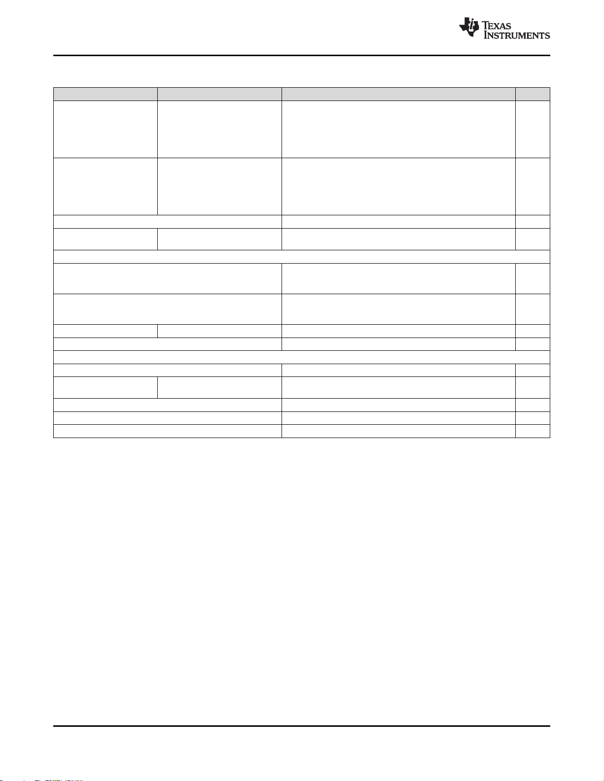
AM3359, AM3358, AM3357, AM3356, AM3354, AM3352, AM3351
SPRS717J –OCTOBER 2011–REVISED APRIL 2016
www.ti.com
Table 5-16. TSC_ADC Electrical Parameters (continued)
PARAMETER TEST CONDITIONS MIN NOM MAX UNIT
Internal voltage reference:
Spurious free dynamic
range
Signal-to-noise plus
distortion
VREFP and VREFN input impedance 20 kΩ
Input impedance of
(2)
AIN[7:0]
Sampling Dynamics
Conversion time 15
Acquisition time 2
Sampling rate ADC clock = 3 MHz 200 kSPS
Channel-to-channel isolation 100 dB
Touch Screen Switch Drivers
Pullup and pulldown switch ON resistance (Ron) 2 Ω
Pullup and pulldown switch
current leakage Ileak
Drive current 25 mA
Touch screen resistance 6 kΩ
Pen touch detect 2 kΩ
(1) VREFP and VREFN must be tied to ground if the internal voltage reference is used.
(2) This parameter is valid when the respective AIN terminal is configured to operate as a general-purpose ADC input.
VDDA_ADC = 1.8 V
External voltage reference:
VREFP – VREFN = 1.8 V
80 dB
Input signal: 30-kHz sine wave at
–0.5-dB full scale
Internal voltage reference:
VDDA_ADC = 1.8 V
External voltage reference:
VREFP – VREFN = 1.8 V
69 dB
Input signal: 30-kHz sine wave at
–0.5-dB full scale
ƒ = Input frequency [1 / ((65.97 × 10
–12
) × ƒ)] Ω
ADC
clock
cycles
ADC
clock
cycles
Source impedance = 500 Ω 0.5 uA
98
Specifications Copyright © 2011–2016, Texas Instruments Incorporated
Submit Documentation Feedback
Product Folder Links: AM3359 AM3358 AM3357 AM3356 AM3354 AM3352 AM3351
Page 99

0
Supply value
t
slew rate < 1E + 5 V/s
slew > (supply value) / (1E + 5V/s)
supply value * 10 µs
AM3359, AM3358, AM3357, AM3356, AM3354, AM3352, AM3351
www.ti.com
6 Power and Clocking
6.1 Power Supplies
6.1.1 Power Supply Slew Rate Requirement
To maintain the safe operating range of the internal ESD protection devices, TI recommends limiting the
maximum slew rate for powering on the supplies to be less than 1.0E +5 V/s. For instance, as shown in
Figure 6-1, TI recommends a value greater than 18 µs for the supply ramp slew for a 1.8-V supply.
Figure 6-1. Power Supply Slew and Slew Rate
SPRS717J –OCTOBER 2011–REVISED APRIL 2016
Product Folder Links: AM3359 AM3358 AM3357 AM3356 AM3354 AM3352 AM3351
Submit Documentation Feedback
Power and ClockingCopyright © 2011–2016, Texas Instruments Incorporated
99
Page 100

VDDS_RTC
RTC_PWRONRSTn
PMIC_POWER_EN
VDDS_DDR
All 1.8-V Supplies
IO 3.3-V Supplies
VDD_CORE, VDD_MPU
PWRONRSTn
CLK_M_OSC
1.8V
1.8V
1.8V
1.8V
1.8V/1.5V/1.35V
3.3V
1.1V
AM3359, AM3358, AM3357, AM3356, AM3354, AM3352, AM3351
SPRS717J –OCTOBER 2011–REVISED APRIL 2016
www.ti.com
A. RTC_PWRONRSTn should be asserted for at least 1 ms to provide enough time for the internal RTC LDO output to
B. When using the ZCZ package option, VDD_MPU and VDD_CORE power inputs may be powered from the same
C. If a USB port is not used, the respective VDDA1P8V_USB terminal may be connected to any 1.8-V power supply and
D. If the system uses mDDR or DDR2 memory devices, VDDS_DDR can be ramped simultaneously with the other 1.8-V
E. VDDS_RTC can be ramped independent of other power supplies if PMIC_POWER_EN functionality is not required. If
F. To configure VDDSHVx [1-6] as 1.8 V, power up the respective VDDSHVx [1-6] to 1.8 V following the recommended
reach a valid level before RTC reset is released.
source if the application only uses operating performance points (OPPs) that define a common power supply voltage
for VDD_MPU and VDD_CORE. The ZCE package option has the VDD_MPU domain merged with the VDD_CORE
domain.
the respective VDDA3P3V_USB terminal may be connected to any 3.3-V power supply. If the system does not have a
3.3-V power supply, the VDDA3P3V_USB terminal may be connected to ground.
IO power supplies.
VDDS_RTC is ramped after VDD_CORE, there might be a small amount of additional leakage current on
VDD_CORE. The power sequence shown provides the lowest leakage option.
sequence. To configure VDDSHVx [1-6] as 3.3 V, power up the respective VDDSHVx [1-6] to 3.3 V following the
recommended sequence.
Figure 6-2. Preferred Power-Supply Sequencing With Dual-Voltage IOs Configured as 3.3 V
100
Power and Clocking Copyright © 2011–2016, Texas Instruments Incorporated
Submit Documentation Feedback
Product Folder Links: AM3359 AM3358 AM3357 AM3356 AM3354 AM3352 AM3351
 Loading...