

CHIP FORM
SG2524, SG3524
REGULATING PULSE-WIDTH MODULATORS
SLVS077B – APRIL 1977 – REVISED JULY 1999
D
Complete PWM Power Control Circuitry
D
Uncommitted Outputs for Single-Ended or
Push-Pull Applications
D
Low Standby Current ...8 mA Typ
D
Interchangeable With Silicon General
SG2524 and SG3524
description
OSC OUT
CURR LIM+
CURR LIM–
The SG2524 and SG3524 incorporate all the
functions required in the construction of a
regulating power supply, inverter, or switching
regulator on a single chip. They also can be used
as the control element for high-power-output
applications. The SG2524 and SG3524 were
designed for switching regulators of either polarity, transformer-coupled dc-to-dc converters, transformerless
voltage doublers, and polarity converter applications employing fixed-frequency, pulse-width-modulation
(PWM) techniques. The complementary output allows either single-ended or push-pull application. Each device
includes an on-chip regulator, error amplifier , programmable oscillator, pulse-steering flip-flop, two uncommitted
pass transistors, a high-gain comparator, and current-limiting and shut-down circuitry.
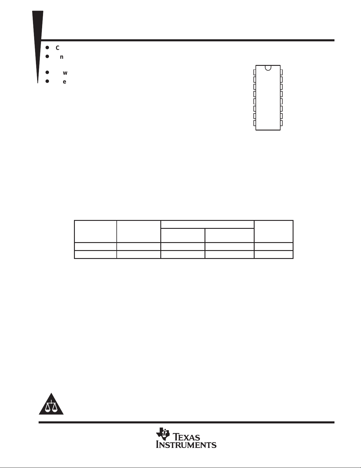
D OR N PACKAGE
(TOP VIEW)
IN–
1
IN+
2
3
4
5
RT
6
CT
7
GND
8
REF OUT
16
V
15
EMIT 2
14
COL 2
13
COL 1
12
EMIT 1
11
SHUTDOWN
10
COMP
9
CC
The SG2524 is characterized for operation from –25°C to 85°C, and the SG3524 is characterized for operation
from 0°C to 70°C.
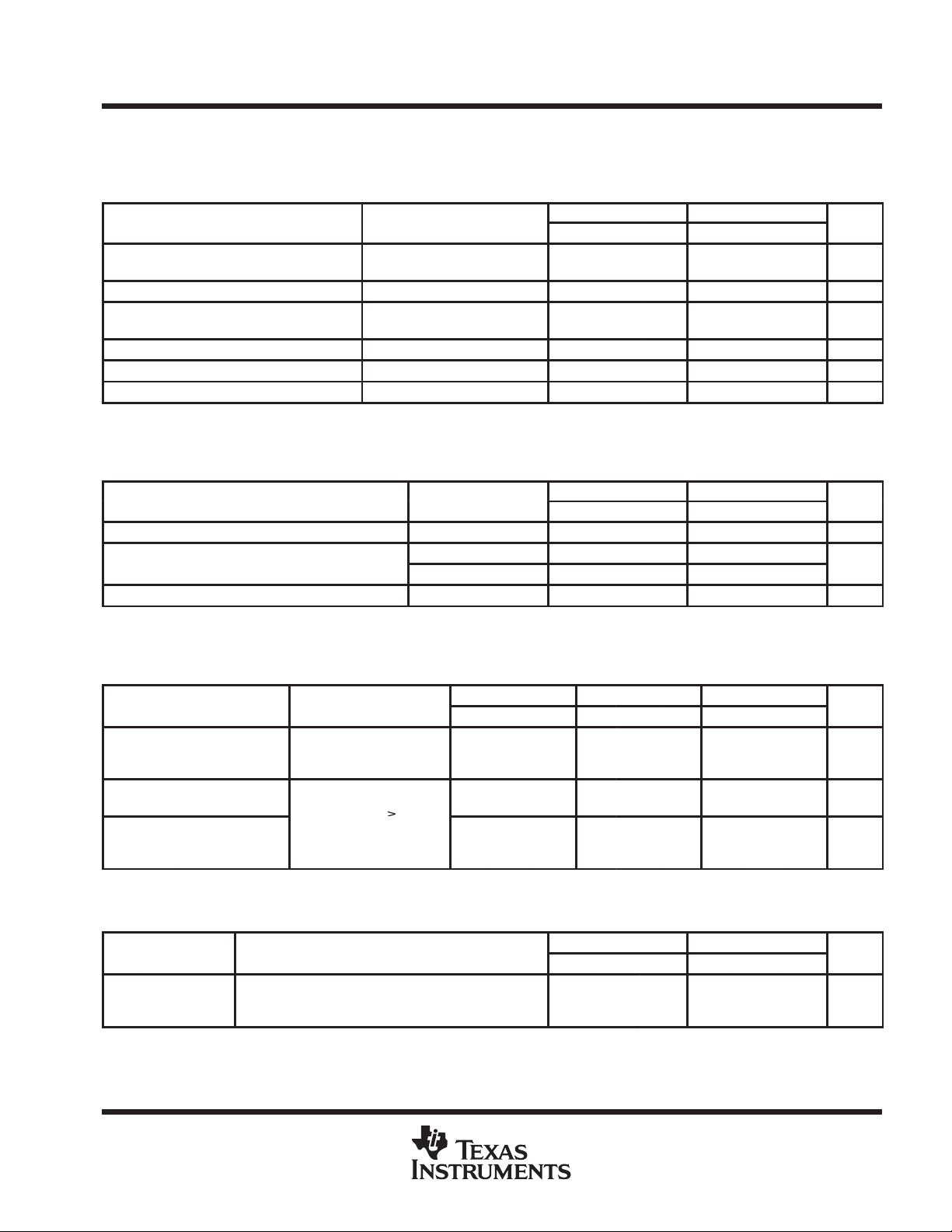
AVAILABLE OPTIONS
INPUT
T
A
0°C to 70°C 30 SG3524D SG3524N SG3524Y
–25°C to 85°C 20 SG2524D SG2524N —
The D package is available taped and reeled. Add the suffix R to the device type (e.g., SG3524DR). Chip
forms are tested at 25°C.
REGULATION
MAX (MV)
SMALL OUTLINE
PACKAGED DEVICES
PLASTIC DIP
(D)
(N)
(Y)
Please be aware that an important notice concerning availability, standard warranty, and use in critical applications of
Texas Instruments semiconductor products and disclaimers thereto appears at the end of this data sheet.
PRODUCTION DATA information is current as of publication date.
Products conform to specifications per the terms of Texas Instruments
standard warranty. Production processing does not necessarily include
testing of all parameters.
POST OFFICE BOX 655303 • DALLAS, TEXAS 75265
Copyright 1999, Texas Instruments Incorporated
1
SG2524, SG3524
REGULATING PULSE-WIDTH MODULATORS
SLVS077B – APRIL 1977 – REVISED JULY 1999
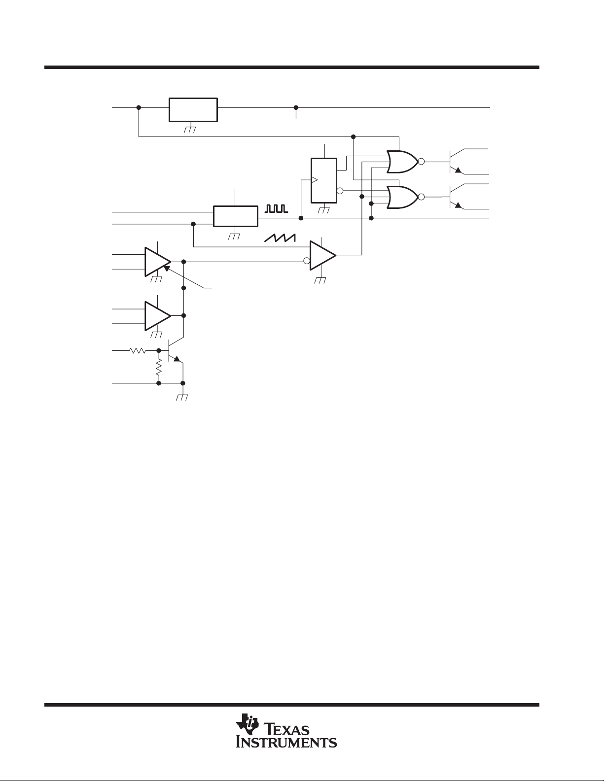
functional block diagram
V
CC
RT
CT
IN–
IN+
COMP
CURR LIM+
CURR LIM –
SHUTDOWN
GND
15
6
7
1
2
9
4
5
10
8
1 kΩ
10 kΩ
+
–
V
–
+
ref
V
Reference
Regulator
ref
V
ref
Oscillator
Error Amplifier
16
REF OUT
V
ref
V
ref
T
V
ref
Comparator
12
11
13
14
3
COL 1
EMIT 1
COL 2
EMIT 2
OSC OUT
NOTE A: Resistor values shown are nominal.
absolute maximum ratings over operating free-air temperature range (unless otherwise noted)
Supply voltage, VCC (see Notes 1 and 2) 40 V. . . . . . . . . . . . . . . . . . . . . . . . . . . . . . . . . . . . . . . . . . . . . . . . . . . . .
Collector output current, ICC 100 mA. . . . . . . . . . . . . . . . . . . . . . . . . . . . . . . . . . . . . . . . . . . . . . . . . . . . . . . . . . . . . .
Reference output current, I
Current through CT terminal –5 mA. . . . . . . . . . . . . . . . . . . . . . . . . . . . . . . . . . . . . . . . . . . . . . . . . . . . . . . . . . . . . . .
Package thermal impedance, θJA (see Notes 3 and 4): D package 112°C/W. . . . . . . . . . . . . . . . . . . . . . . . . .
Lead temperature 1,6 mm (1/16 inch) from case for 10 seconds 260°C. . . . . . . . . . . . . . . . . . . . . . . . . . . . . . .
Storage temperature range, T
†
Stresses beyond those listed under “absolute maximum ratings” may cause permanent damage to the device. These are stress ratings only, and
functional operation of the device at these or any other conditions beyond those indicated under “recommended operating conditions” is not
implied. Exposure to absolute-maximum-rated conditions for extended periods may affect device reliability.
NOTES: 1. All voltage values are with respect to network ground terminal.
2. The reference regulator may be bypassed for operation from a fixed 5-V supply by connecting the VCC and reference output pin
both to the supply voltage. In this configuration, the maximum supply voltage is 6 V .
3. Maximum power dissipation is a function of T
allowable ambient temperature is PD = (T
impact reliability.
4. The package thermal impedance is calculated in accordance with JESD 51, except for through-hole packages which use a trace
length of zero.
50 mA. . . . . . . . . . . . . . . . . . . . . . . . . . . . . . . . . . . . . . . . . . . . . . . . . . . . . . . . . . .
O(ref)
N package 88°C/W. . . . . . . . . . . . . . . . . . . . . . . . . . . .
–65°C to 150°C. . . . . . . . . . . . . . . . . . . . . . . . . . . . . . . . . . . . . . . . . . . . . . . . . . .
stg
,
θ
J(max)
J(max)
– TA)/
, and TA. The maximum allowable power dissipation at any
JA
θ
. Operation at the absolute maximum TJ of 150°C can
JA
†
2
POST OFFICE BOX 655303 • DALLAS, TEXAS 75265
UNIT
PARAMETER
TEST CONDITIONS
†
UNIT
SG2524, SG3524
REGULATING PULSE-WIDTH MODULATORS
SLVS077B – APRIL 1977 – REVISED JULY 1999
recommended operating conditions
SG2524 SG3524
MIN MAX MIN MAX
Supply voltage, V
Reference output current 0 50 0 50 mA
Current through CT terminal –0.03 –2 –0.03 –2 mA
Timing resistor , R
Timing capacitor , C
Operating free-air temperature –25 85 0 70 °C
CC
T
T
electrical characteristics over recommended operating free-air temperature range, VCC = 20 V,
f = 20 kHz (unless otherwise noted)
reference section
SG2524 SG3524 SG3524Y
MIN TYP‡MAX MIN TYP‡MAX MIN TYP‡MAX
Output voltage 4.8 5 5.2 4.6 5 5.4 5 V
Input regulation VCC = 8 V to 40 V 10 20 10 30 10 mV
Ripple rejection f = 120 Hz 66 66 66 dB
Output regulation IO = 0 mA to 20 mA 20 50 20 50 20 mV
Output voltage change
with temperature
Short-circuit output
§
current
†
For conditions shown as MIN or MAX, use the appropriate value specified under recommended operating conditions.
‡
All typical values, except for temperature coefficients, are at TA = 25°C
§
Standard deviation is a measure of the statistical distribution about the mean as derived from the formula:
TA = MIN to MAX 0.3% 1% 0.3% 1%
V
= 0 100 100 100 mA
ref
N
ȍ
Ǹ
s
+
(xn*
n+1
N*1
X)
2
8 40 8 40 V
1.8 100 1.8 100 kΩ
0.001 0.1 0.001 0.1 µF
POST OFFICE BOX 655303 • DALLAS, TEXAS 75265
3
SG2524, SG3524
PARAMETER
TEST CONDITIONS
†
UNIT
∆f
PARAMETER
TEST
UNIT
REGULATING PULSE-WIDTH MODULATORS
SLVS077B – APRIL 1977 – REVISED JULY 1999
electrical characteristics over recommended operating free-air temperature range, VCC = 20 V,
f = 20 kHz (unless otherwise noted)
oscillator section
SG2524, SG3524 SG3524Y
MIN TYP‡MAX MIN TYP‡MAX
f
Oscillator frequency CT = 0.001 µF, RT = 2 kΩ 450 450 kHz
osc
Standard deviation of
frequency
Frequency change with
voltage
osc
Frequency change with
temperature
Output amplitude at OSC
OUT
Output pulse duration
t
w
(width) at OSC OUT
†
For conditions shown as MIN or MAX, use the appropriate value specified under recommended operating conditions.
‡
All typical values, except for temperature coefficients, are at TA = 25°C
§
Standard deviation is a measure of the statistical distribution about the mean as derived from the formula:
§
All values of voltage, temperature,
resistance, and capacitance constant
VCC = 8 V to 40 V, TA = 25°C 1% 1%
TA = MIN to MAX 2%
TA = 25°C 3.5 3.5 V
CT = 0.01 µF, TA = 25°C 0.5 0.5 µs
N
ȍ
Ǹ
s
+
(xn*
n+1
N*1
X)
2
5% 5%
error amplifier section
TEST
CONDITIONS
V
I
IB
V
CMMR
B
†
For conditions shown as MIN or MAX, use the appropriate value specified under recommended operating conditions.
‡
All typical values, except for temperature coefficients, are at TA = 25°C
Input offset voltage VIC = 2.5 V 0.5 5 2 10 2 mV
IO
Input bias current VIC = 2.5 V 2 10 2 10 2 µA
Open-loop voltage
amplification
Common-mode input
ICR
voltage range
Common-mode rejection
ratio
Unity-gain bandwidth 3 3 3 MHz
1
Output swing TA = 25°C 0.5 3.8 0.5 3.8 0.5 3.8 V
TA = 25°C
†
SG2524 SG3524 SG3524Y
MIN TYP‡MAX MIN TYP‡MAX MIN TYP‡MAX
72 80 60 80 80 dB
1.8 to
3.4
70 70 70 dB
1.8 to
3.4
V
4
POST OFFICE BOX 655303 • DALLAS, TEXAS 75265
PARAMETER
TEST CONDITIONS
†
UNIT
PARAMETER
TEST CONDITIONS
†
UNIT
VITInput threshold voltage at COMP
V
PARAMETER
TEST CONDITIONS
UNIT
V
(IN+)
V
(IN–)
PARAMETER
TEST CONDITIONS
UNIT
SG2524, SG3524
REGULATING PULSE-WIDTH MODULATORS
SLVS077B – APRIL 1977 – REVISED JULY 1999
electrical characteristics over recommended operating free-air temperature range, VCC = 20 V,
f = 20 kHz (unless otherwise noted)
output section
SG2534, SG3524 SG3524Y
MIN TYP‡MAX MIN TYP‡MAX
V
(BR)CE
V
sat
V
O
t
r
t
f
†
For conditions shown as MIN or MAX, use the appropriate value specified under recommended operating conditions.
‡
All typical values, except for temperature coefficients, are at TA = 25°C.
comparator section
I
IB
†
For conditions shown as MIN or MAX, use the appropriate value specified under recommended operating conditions.
‡
All typical values, except for temperature coefficients, are at TA = 25°C.
Collector-emitter breakdown
voltage
Collector off-state current VCE = 40 V 0.01 50 0.01 µA
Collector-emitter saturation
voltage
Emitter output voltage VC = 20 V, IE = –250 µA 17 18 18 V
Turn-off voltage rise time RC = 2 kΩ 0.2 0.2 µs
Turn-on voltage fall time RC = 2 kΩ 0.1 0.1 µs
Maximum duty cycle, each output 45%
p
Input bias current –1 –1 µA
IC = 50 mA 1 2 1 V
Zero duty cycle 1 1
Maximum duty cycle 3.5 3.5
40 V
SG2534, SG3524 SG3524Y
MIN TYP‡MAX MIN TYP‡MAX
current limiting section
MIN TYP‡MAX MIN TYP†MAX MIN TYP†MAX
Input voltage
V
I
V
(SENSE)
‡
All typical values, except for temperature coefficients, are at TA = 25°C.
range
(either input)
Sense voltage
at TA = 25°C
Temperature
coefficient of
sense voltage
V
(COMP)
–
≥ 50 mV,
= 2 V
–1
175 200 225 175 200 225 175 200 225 mV
total device
Standby
I
st
current
‡
All typical values, except for temperature coefficients, are at TA = 25°C.
VCC = 40 V, IN–, CURR LIM+, CT, GND, COMP,
EMIT 1, EMIT 2 grounded, IN+ at 2 V,
All other inputs and outputs open
SG2524 SG3524 SG3524Y
to
1
0.2 0.2 0.2 mV/°C
–1
to
1
SG2524, SG3524 SG3524Y
MIN TYP‡MAX MIN TYP‡MAX
8 10 8 mA
V
POST OFFICE BOX 655303 • DALLAS, TEXAS 75265
5

SG2524, SG3524
REGULATING PULSE-WIDTH MODULATORS
SLVS077B – APRIL 1977 – REVISED JULY 1999
PARAMETER MEASUREMENT INFORMATION
2 kΩ
10 kΩ
2 kΩ
V
1 kΩ
REF
VCC = 8 V to 40 V
15
V
2 kΩ10 kΩ
C
T
R
T
SG2524 or SG3524
10
SHUTDOWN
2
IN+
1
IN–
9
COMP
4
CURR LIM+
5
CURR LIM–
7
C
T
6
R
T
CC
GND
8
OSC OUT
REF OUT
COL 2
COL 1
EMIT 2
EMIT 1
3
16
13
12
14
11
(Open)
V
REF
0.1 µF
2 kΩ
1 W
2 kΩ
1 W
Outputs
Figure 1. General Test Circuit
Circuit Under Test
TEST CIRCUIT
V
CC
2 kΩ
Output
Output
90%
t
f
10%
VOLTAGE WAVEFORMS
10%
t
r
90%
≈V
≈0 V
CC
Figure 2. Switching Times
6
POST OFFICE BOX 655303 • DALLAS, TEXAS 75265

SG2524, SG3524
REGULATING PULSE-WIDTH MODULATORS
SLVS077B – APRIL 1977 – REVISED JULY 1999
TYPICAL CHARACTERISTICS
OPEN-LOOP VOLTAGE AMPLIFICATION
90
80
70
60
50
40
30
RL = ∞
OF ERROR AMPLIFIER
RL = 1 MΩ
RL = 300 kΩ
RL = 100 kΩ
RL = 30 kΩ
vs
FREQUENCY
VCC = 20 V
TA = 25°C
1M
400 k
100 k
40 k
10 k
4 k
OSCILLATOR FREQUENCY
vs
TIMING RESISTANCE
CT = 0
CT = 0.001 µF
CT = 0.003 µF
CT = 0.01 µF
20
10
0
RL is resistance from COMP to ground
–10
Open-Loop Voltage Amplification of Error Amplifier – dB
Frequency – Hz
Figure 3
10
4
µs
1
0.4
Output Dead Time –
– Oscillator Frequency – Hz
1 k
osc
f
400
10 M1 M100 k10 k1 k100
100
1
OUTPUT DEAD TIME
vs
TIMING CAPACITANCE
CT = 0.03 µF
CT = 0.1 µF
VCC = 20 V
TA = 25°C
20 40 1007010742
RT – Timing Resistance – kΩ
Figure 4
0.1
0.001 0.01
0.004 0.10.04
CT – Timing Capacitance – µF
Figure 5
POST OFFICE BOX 655303 • DALLAS, TEXAS 75265
7

SG2524, SG3524
REGULATING PULSE-WIDTH MODULATORS
SLVS077B – APRIL 1977 – REVISED JULY 1999
PRINCIPLES OF OPERATION
The SG2524 is a fixed-frequency pulse-width-modulation voltage-regulator control circuit. The regulator operates at
a fixed frequency that is programmed by one timing resistor, RT, and one timing capacitor, CT. RT establishes a
constant charging current for C
linear control of the output pulse duration (width) by the error amplifier. The SG2524 contains an onboard 5-V
regulator that serves as a reference, as well as supplying the SG2524 internal regulator control circuitry . The internal
reference voltage is divided externally by a resistor ladder network to provide a reference within the common-mode
range of the error amplifier as shown in Figure 6, or an external reference can be used. The output is sensed by a
second resistor divider network and the error signal is amplified. This voltage is then compared to the linear voltage
ramp at C
pass transistor (Q1 or Q2) by the pulse-steering flip-flop, which is synchronously toggled by the oscillator output. The
oscillator output pulse also serves as a blanking pulse to ensure both outputs are never on simultaneously during
the transition times. The duration of the blanking pulse is controlled by the value of CT. The outputs may be applied
in a push-pull configuration in which their frequency is half that of the base oscillator, or paralleled for single-ended
applications in which the frequency is equal to that of the oscillator. The output of the error amplifier shares a common
input to the comparator with the current-limiting and shut-down circuitry and can be overridden by signals from either
of these inputs. This common point also is available externally and can be employed to control the gain of, to
compensate the error amplifier, or to provide additional control to the regulator.
. The resulting modulated pulse out of the high-gain comparator is then steered to the appropriate output
T
. This results in a linear voltage ramp at CT, which is fed to the comparator providing
T
APPLICATION INFORMATION
†
†
oscillator
The oscillator controls the frequency of the SG2524 and is programmed by RT and CT as shown in Figure 4.
1.30
f
[
RTC
T
where: RT is in kΩ
C
is in µF
T
f is in kHz
Practical values of C
results in a frequency range typically from 130 Hz to 722 kHz.
fall between 0.001 and 0.1 µF. Practical values of RT fall between 1.8 and 100 kΩ. This
T
blanking
The output pulse of the oscillator is used as a blanking pulse at the output. This pulse duration is controlled by
the value of CT as shown in Figure 5. If small values of CT are required, the oscillator output pulse duration can
still be maintained by applying a shunt capacitance from OSC OUT to ground.
synchronous operation
When an external clock is desired, a clock pulse of approximately 3 V can be applied directly to the oscillator
output terminal. The impedance to ground at this point is approximately 2 kΩ. In this configuration, RT CT must
be selected for a clock period slightly greater than that of the external clock.
†
Throughout these discussions, references to the SG2524 apply also to the SG3524.
8
POST OFFICE BOX 655303 • DALLAS, TEXAS 75265

SG2524, SG3524
REGULATING PULSE-WIDTH MODULATORS
SLVS077B – APRIL 1977 – REVISED JULY 1999
APPLICATION INFORMATION
†
synchronous operation (continued)
If two or more SG2524 regulators are operated synchronously, all oscillator output terminals must be tied
together. The oscillator programmed for the minimum clock period is the master from which all the other
SG2524s operate. In this application, the CTRT values of the slaved regulators must be set for a period
approximately 10% longer than that of the master regulator. In addition, CT (master) = 2 CT (slave) to ensure
that the master output pulse, which occurs first, has a longer pulse duration and subsequently resets the slave
regulators.
voltage reference
The 5-V internal reference can be employed by use of an external resistor divider network to establish a
reference common-mode voltage range (1.8 V to 3.4 V) within the error amplifiers as shown in Figure 6, or an
external reference can be applied directly to the error amplifier. For operation from a fixed 5-V supply , the internal
reference can be bypassed by applying the input voltage to both the VCC and V
configuration, however, the input voltage is limited to a maximum of 6 V.
REF OUT
5 kΩ
2.5 V
R25 kΩ
R1
To Positive
Output Voltage
+
–
5 kΩ
5 kΩ
R1
2.5 V
R2
REF OUT
+
–
To Negative
Output Voltage
terminals. In this
REF
VO+
2.5V
R1)R2
R1
VO+
2.5Vǒ1
*
R2
R1
Ǔ
Figure 6. Error-Amplifier Bias Circuits
error amplifier
The error amplifier is a differential-input transconductance amplifier . The output is available for dc gain control
or ac phase compensation. The compensation node (COMP) is a high-impedance node (R
= 5 MΩ). The gain
L
of the amplifier is AV = (0.002 Ω–1)RL and can easily be reduced from a nominal 10,000 by an external shunt
resistance from COMP to ground. Refer to Figure 3 for data.
compensation
COMP , as discussed above, is made available for compensation. Since most output filters introduce one or more
additional poles at frequencies below 200 Hz, which is the pole of the uncompensated amplifier, introduction
of a zero to cancel one of the output filter poles is desirable. This can best be accomplished with a series RC
circuit from COMP to ground in the range of 50 kΩ and 0.001
of the formula f ≈ 1/RC.
†
Throughout these discussions, references to the SG2524 apply also to the SG3524.
µF. Other frequencies can be canceled by use
POST OFFICE BOX 655303 • DALLAS, TEXAS 75265
9

SG2524, SG3524
REGULATING PULSE-WIDTH MODULATORS
SLVS077B – APRIL 1977 – REVISED JULY 1999
APPLICATION INFORMATION
†
shut-down circuitry
COMP can also be employed to introduce external control of the SG2524. Any circuit that can sink 200 µA can
pull the compensation terminal to ground and thus disable the SG2524.
In addition to constant-current limiting, CURR LIM+ and CURR LIM– may also be used in transformer-coupled
circuits to sense primary current and shorten an output pulse should transformer saturation occur. CURR LIM–
may also be grounded to convert CURR LIM+ into an additional shut-down terminal.
current limiting
A current-limiting sense amplifier is provided in the SG2524. The current-limiting sense amplifier exhibits a
threshold of 200 mV ±25 mV and must be applied in the ground line since the voltage range of the inputs is
limited to 1 V to –1 V . Caution should be taken to ensure the –1 V limit is not exceeded by either input, otherwise
damage to the device may result.
Foldback current limiting can be provided with the network shown in Figure 7. The current-limit schematic is
shown in Figure 8.
EMIT 1
EMIT 2
SG2524
CURR LIM–
CURR LIM+
11
14
5
4
R1
R2
R
s
V
O
I
O(max)
IOS+
1
+
R
s
200 mV
R
s
ǒ
200 mV
)
R1)R2
VOR2
Ǔ
Figure 7. Foldback Current Limiting for Shorted Output Conditions
COMP
Error Amplifier
CURR LIM–
Constant-Current Source
CURR LIM+
Figure 8. Current-Limit Schematic
†
Throughout these discussions, references to the SG2524 apply also to the SG3524.
C
T
Comparator
10
POST OFFICE BOX 655303 • DALLAS, TEXAS 75265

SG2524, SG3524
REGULATING PULSE-WIDTH MODULATORS
SLVS077B – APRIL 1977 – REVISED JULY 1999
APPLICATION INFORMATION
†
output circuitry
The SG2524 contains two identical npn transistors, the collectors and emitters of which are uncommitted. Each
transistor has antisaturation circuitry that limits the current through that transistor to a maximum of 100 mA for
fast response.
general
There are a wide variety of output configurations possible when considering the application of the SG2524 as
a voltage regulator control circuit. They can be segregated into three basic categories:
1. Capacitor-diode-coupled voltage multipliers
2. Inductor-capacitor-implemented single-ended circuits
3. Transformer-coupled circuits
Examples of these categories are shown in Figures 9, 10 and 11 respectively. Detailed diagrams of specific
applications are shown in Figures 12 through 15.
D1
V
V
I
O
VI > V
O
D1
V
V
I
D1
V
I
O
VI < V
O
–V
O
| +VI | > | – VO |
Figure 9. Capacitor-Diode-Coupled Voltage-Multiplier Output Stages
†
Throughout these discussions, references to the SG2524 apply also to the SG3524.
POST OFFICE BOX 655303 • DALLAS, TEXAS 75265
11

SG2524, SG3524
REGULATING PULSE-WIDTH MODULATORS
SLVS077B – APRIL 1977 – REVISED JULY 1999
APPLICATION INFORMATION
V
I
V
I
V
I
V
VI > V
V
VI < V
–VO
| +VI | < | – VO |
†
O
O
O
O
V
I
PUSH-PULL
Figure 10. Single-Ended Inducor Circuit
V
I
V
O
Figure 11. Transformer-Coupled Outputs
FLYBACK
V
O
†
Throughout these discussions, references to the SG2524 apply also to the SG3524.
12
POST OFFICE BOX 655303 • DALLAS, TEXAS 75265

SG2524, SG3524
REGULATING PULSE-WIDTH MODULATORS
SLVS077B – APRIL 1977 – REVISED JULY 1999
5 kΩ
0.1 µF
0.01 µF
5 kΩ
15 kΩ
5 kΩ
2 kΩ
APPLICATION INFORMATION
VCC = 15 V
15
V
1
IN–
2
IN+
16
REF OUT
6
R
T
7
C
T
10
SHUTDOWN
3
OSC OUT
CC
SG2524
CURR LIM+
CURR LIM–
GND
8
EMIT 1
COL 1
COL 2
EMIT 2
.
COMP
1N916
11
12
13
14
4
5
9
†
Figure 11. Capacitor-Diode Output Circuit
–5 V
20 mA
1N91620 µF
+
1N916
+
50 µF
+
100 µF
Input
Return
25 kΩ
5 kΩ
5 kΩ
0.02 µF
2 kΩ
5 kΩ
1
IN–
2
IN+
16
REF OUT
6
R
T
7
C
T
10
SHUTDOWN
3
OSC OUT
VCC = 5 V
15
V
CC
SG2524
CURR LIM+
CURR LIM–
GND
8
EMIT 1
COL 1
COL 2
EMIT 2
COMP
11
12
13
14
4
5
9
300 Ω
1 MΩ
1N916
0.001 µF
4.7 µF
+
Figure 12. Flyback Converter Circuit
200 Ω
0.1 µF
2N2222
20T
510 Ω
1N916
50T
50T
620 Ω
50 µF
50 µF
1N916
TIP29A
1 Ω
15 V
+
20 mA
+
–15 V
†
Throughout these discussions, references to the SG2524 apply also to the SG3524.
POST OFFICE BOX 655303 • DALLAS, TEXAS 75265
13

SG2524, SG3524
REGULATING PULSE-WIDTH MODULATORS
SLVS077B – APRIL 1977 – REVISED JULY 1999
5 kΩ
0.1 µF
0.02 µF
5 kΩ
3 kΩ
5 kΩ
5 kΩ
APPLICATION INFORMATION
VCC = 28 V
15
V
T
T
CC
SG2524
CURR LIM+
CURR LIM–
GND
8
EMIT 1
COL 1
COL 2
EMIT 2
COMP
11
12
13
14
4
5
9
0.001 µF
50 kΩ
1
2
16
6
7
10
3
IN–
IN+
REF OUT
R
C
SHUT
DOWN
OSC OUT
†
TIP115
3 kΩ
Input Return
0.9 mH
1N3880
0.1 Ω
+
500 µF
5 V
1 A
5 kΩ
0.1 µF
0.01 µF
5 kΩ
2 kΩ
5 kΩ
5 kΩ
1
2
16
6
7
10
3
VCC = 28 V
IN–
SG2524
IN+
REF OUT
R
T
C
T
SHUT
DOWN
OSC OUT
Figure 13. Single-Ended LC Circuit
15
V
CC
EMIT 1
COL 1
COL 2
EMIT 2
CURR LIM+
CURR LIM–
COMP
GND
8
1 kΩ
1W
11
12
13
14
4
5
9
1 kΩ
100 Ω
0.001 µF
20 kΩ
1W
TIP31A
100 Ω
TIP31A
0.1 Ω
TIR101A
1 mH
20T
20T
+
5T
5T
100 µF
1500 µF
+
+
5 V
5 A
–
Figure 14. Push-Pull Transformer-Coupled Circuit
†
Throughout these discussions, references to the SG2524 apply also to the SG3524.
14
POST OFFICE BOX 655303 • DALLAS, TEXAS 75265

IMPORTANT NOTICE
T exas Instruments and its subsidiaries (TI) reserve the right to make changes to their products or to discontinue
any product or service without notice, and advise customers to obtain the latest version of relevant information
to verify, before placing orders, that information being relied on is current and complete. All products are sold
subject to the terms and conditions of sale supplied at the time of order acknowledgement, including those
pertaining to warranty, patent infringement, and limitation of liability.
TI warrants performance of its semiconductor products to the specifications applicable at the time of sale in
accordance with TI’s standard warranty. Testing and other quality control techniques are utilized to the extent
TI deems necessary to support this warranty . Specific testing of all parameters of each device is not necessarily
performed, except those mandated by government requirements.
CERTAIN APPLICA TIONS USING SEMICONDUCT OR PRODUCTS MAY INVOLVE POTENTIAL RISKS OF
DEATH, PERSONAL INJURY, OR SEVERE PROPERTY OR ENVIRONMENTAL DAMAGE (“CRITICAL
APPLICATIONS”). TI SEMICONDUCTOR PRODUCTS ARE NOT DESIGNED, AUTHORIZED, OR
WARRANTED TO BE SUITABLE FOR USE IN LIFE-SUPPORT DEVICES OR SYSTEMS OR OTHER
CRITICAL APPLICA TIONS. INCLUSION OF TI PRODUCTS IN SUCH APPLICATIONS IS UNDERST OOD TO
BE FULLY AT THE CUSTOMER’S RISK.
In order to minimize risks associated with the customer’s applications, adequate design and operating
safeguards must be provided by the customer to minimize inherent or procedural hazards.
TI assumes no liability for applications assistance or customer product design. TI does not warrant or represent
that any license, either express or implied, is granted under any patent right, copyright, mask work right, or other
intellectual property right of TI covering or relating to any combination, machine, or process in which such
semiconductor products or services might be or are used. TI’s publication of information regarding any third
party’s products or services does not constitute TI’s approval, warranty or endorsement thereof.
Copyright 1999, Texas Instruments Incorporated
 Loading...