

Page 1
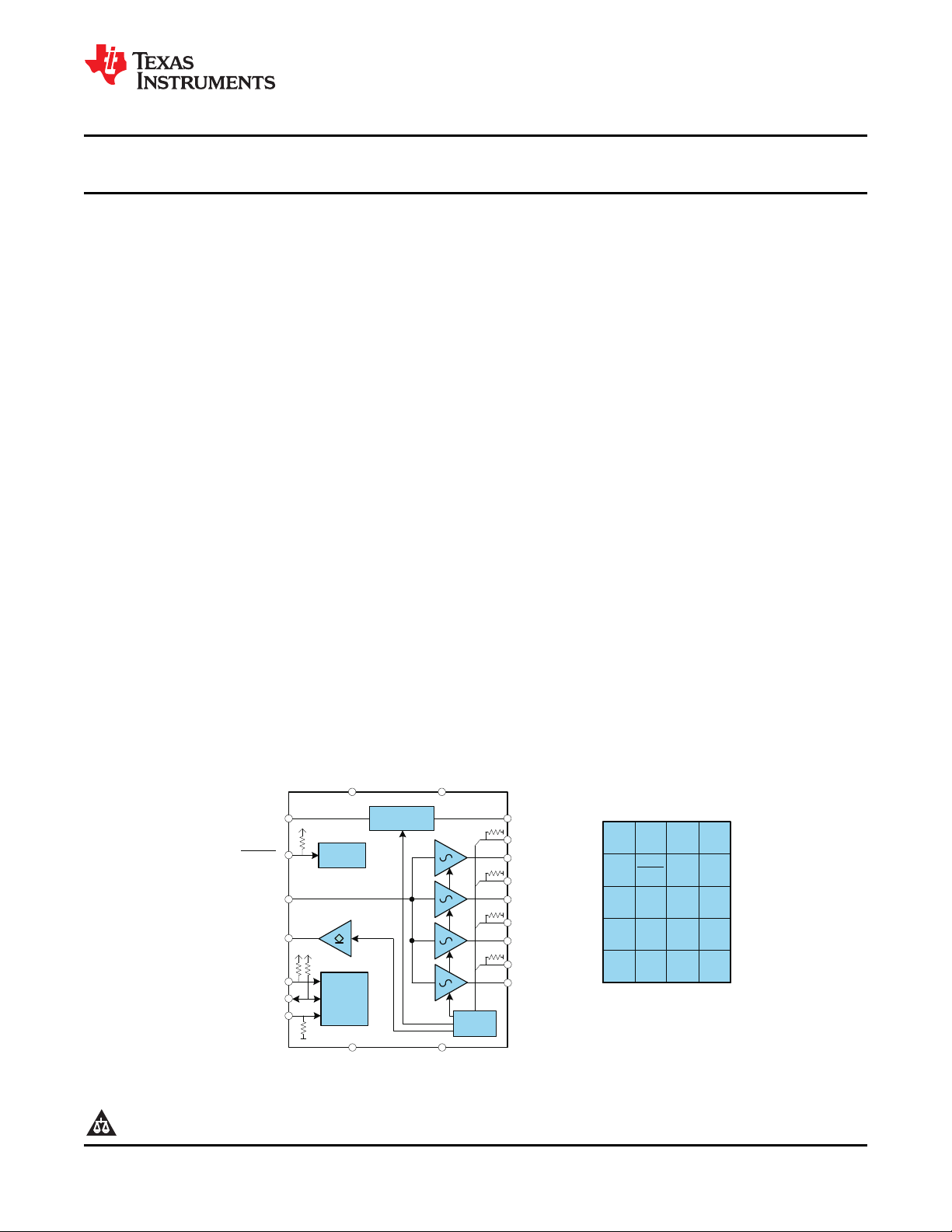
VDD_ANA
LDO
VBAT
MCLK_IN
VLDO
REQ1
CLK1
REQ2
CLK2
REQ3
CLK3
VDD_DIG
I C
2
Control
Register
ADR_A0
MCLK_REQ
SCLH
SDAH
GND_ANA
GND_DIG
RESET
Reset
REQ4
CLK4
Decoder
1 2
D
C
A
WCSP
B
TopView
(SolderBallUnderneath)
3
4
E
CLK1CLK2
REQ1
CLK3
CLK4
REQ3
GND_
DIG
VLDO
REQ4
REQ2
ADR_
A0
VDD_
DIG
MCLK_
IN
MCLK_
REQ
RESET
VDD_
ANA
GND_
ANA
SCLHVBAT SDAH
www.ti.com
CDC3S04
SCAS883A –OCTOBER 2009–REVISED JULY 2010
Quad Sine-Wave Clock Buffer With LDO
Check for Samples: CDC3S04
1
FEATURES
• 1:4 Low-Jitter Clock Buffer
• Single-Ended Sine-Wave Clock Input and
Outputs
• Ultralow Phase Noise and Standby Current
• Individual Clock Request Inputs for Each
Output
• On-Chip Low-Dropout Output (LDO) for
Low-Noise TCXO Supply
• Serial I2C Interface (Compatible With
High-Speed Mode, 3.4 Mbit/s)
• 1.8-V Device Power Supply
• Wide Temperature Range, –30°C to 85°C
• ESD Protection: 2 KV HBM, 750 V CDM, and
100 V MM
• Small 20-Pin Chip-Scale Package: 0.4-mm
DESCRIPTION
The CDC3S04 is a four-channel low-power low-jitter
sine-wave clock buffer. It can be used to buffer a
single master clock to multiple peripherals. The four
sine-wave outputs (CLK1–CLK4) are designed for
minimal channel-to-channel skew and ultralow
additive output jitter.
Each output has its own clock request inputs which
enables the dedicated clock output. These clock
requests are active-high (can also be changed to be
active-low via I2C), and an output signal is generated
that can be sent back to the master clock to request
the clock (MCLK_REQ). MCKL_REQ is an
open-source output and supports the wired-OR
function (default mode). It needs an external pulldown
resistor. MCKL_REQ can be changed to wired-AND
or push-pull functionality via I2C.
The CDC3S04 also provides an I2C interface
Pitch WCSP (1.6 mm × 2 mm) (Hs-mode) that can be used to enable or disable the
outputs, select the polarity of the REQ inputs, and
APPLICATIONS
• Cellular Phones
• Smart Phones
• Mobile Handsets
• Portable Systems
allow control of internal decoding.
The CDC3S04 features an on-chip high-performance
LDO that accepts voltages from 2.3 V to 5.5 V and
outputs a 1.8-V supply. This 1.8-V supply can be
used to power an external 1.8-V TCXO. It can be
enabled or disabled for power saving at the TCXO.
• Wireless Modems Including GPS, WLAN,
W-BT, D-TV, DVB-H, FM Radio, WiMAX, and
System Clock
1
Please be aware that an important notice concerning availability, standard warranty, and use in critical applications of Texas
Instruments semiconductor products and disclaimers thereto appears at the end of this data sheet.
PRODUCTION DATA information is current as of publication date.
Products conform to specifications per the terms of the Texas
Instruments standard warranty. Production processing does not
necessarily include testing of all parameters.
Copyright © 2009–2010, Texas Instruments Incorporated
Page 2
CDC3S04
SCAS883A –OCTOBER 2009–REVISED JULY 2010
This integrated circuit can be damaged by ESD. Texas Instruments recommends that all integrated circuits be handled with
appropriate precautions. Failure to observe proper handling and installation procedures can cause damage.
ESD damage can range from subtle performance degradation to complete device failure. Precision integrated circuits may be more
susceptible to damage because very small parametric changes could cause the device not to meet its published specifications.
DESCRIPTION (CONTINUED)
A low signal at the RESET input switches the outputs CLK1 and CLK4 into the default state. In this configuration,
CLK1 and CLK4 are ON (see Table 1); the remaining device function is not affected. Also, the RESET input
provides a glitch filter which rejects spikes of typical 300 ns on the RESET line to preserve false reset. A
complete device reset to the default condition can be initiated by a power-up cycle of V
The CDC3S04 operates from two 1.8-V supplies. There is a core supply (VDD_DIG/GND_DIG) for the core logic
and a low-noise analog supply (VDD_ANA/GND_ANA) for the sine-wave outputs. The CDC3S04 is designed for
sequence-less power up. Both supply voltages may be applied in any order.
The CDC3S04 is offered in a 0.4-mm pitch WCSP package (1.6 mm × 2 mm) and is optimized for low standby
current (0.5 µA). It is characterized for operation from –30°C to 85°C.
DEVICE INFORMATION
PIN FUNCTIONS
NAME BALL NO. TYPE FUNCTION
ADR_A0 D4 Input Selectable address bit A0 of slave-address register; internal 500-kΩ pulldown resistor
CLK1 A4 Output Clock output 1
CLK2 A2 Output Clock output 2
CLK3 C4 Output Clock output 3
CLK4 C2 Output Clock output 4
GND_ANA B4 Ground Ground for sine-wave buffer
GND_DIG D2 Ground Ground for core logic
MCLK_IN B1 Input Master clock input
MCLK_RE Clock request to the master clock source; active-high; open-source output for wired-OR
Q connection (default condition). Can be changed to push-pull output or wired-AND output via I2C.
REQ1 A3 Input Clock request from peripheral 1; internal 500-kΩ pulldown resistor
REQ2 A1 Input Clock request from peripheral 2; internal 500-kΩ pulldown resistor
REQ3 C3 Input Clock request from peripheral 3; internal 500-kΩ pulldown resistor
REQ4 C1 Input Clock request from peripheral 4; internal 500-kΩ pulldown resistor
RESET B2 Input CLK1 and CLK4 outputs to ON (see Table 1). On-chip LDO is enabled. Internal 1-MΩ pullup
SCLH E4 Input I2C clock input – Hs-mode. Internal 1-MΩ pullup resistor
SDAH E3 Input/output I2C data input/output – Hs-mode. Internal 1-MΩ pullup resistor
VBAT E2 Power Supply pin to internal LDO
VDD_ANA B3 Power 1.8-V power supply for sine-wave buffer
VDD_DIG D1 Power
VLDO E1 Output
D3 Output
Peripheral reset signal provided by application processor. The signal is active-low and switches
resistor and 300-ns (typ) glitch filter.
1.8-V power supply for core logic. Power up of VDD_DIG resets the whole device to the default
condition.
1.8-V supply for external TCXO; LDO is enabled if RESET (default mode) or REQx is active.
LDO is not enabled if only VBAT is on.
DD_DIG
.
www.ti.com
2 Submit Documentation Feedback Copyright © 2009–2010, Texas Instruments Incorporated
Product Folder Link(s) :CDC3S04
Page 3
www.ti.com
FUNCTION SELECTION TABLES
CDC3S04
SCAS883A –OCTOBER 2009–REVISED JULY 2010
Table 1. Reset and Request (REQx) Conditions for Clock Outputs
(2)
RESET
0 On On
1
PRIORITY BIT
(3)
0 Controlled by REQ2 Controlled by REQ3
1 Controlled by REQ2INT Controlled by REQ3INT
0 Controlled by REQ1 Controlled by REQ2 Controlled by REQ3 Controlled by REQ4
1 Controlled by REQ1INT Controlled by REQ2INT Controlled by REQ3INT Controlled by REQ4INT
CLK1 CLK2 CLK3 CLK4
(1)
(1) Shaded cells show the default setting after power up.
(2) RESET resets REQ1PRIO/REQ4PRIO and REQ1INT/REQ4INT bits to their default values (CLK1/4 is ON) but does not change the
remaining internal SW bits. During RESET, any I2C operation is blocked until RESET is deactivated. A minimum pulse duration of
500 ns must be applied to activate RESET (the internal glitch-filter suppresses spikes of typical 300 ns).
(3) Priority bit defines if the external control pins (HW controlled) or the SW bits (SW controlled) have priority. It can be set in the
configuration register, Byte 2, Bits 0–3.
(1)
(3)
REQ-Signals
Table 2. Request Signal Condition for Clock Outputs
(2)
REQx CLKx
(REQ1/2/3/4) (CLK1/2/3/4)
MCLK_REQ LDO
Active-low 0 Clock High On
1 Disabled to high Low (if all REQx are high) Off (if all REQx are high)
Active-high
0 Disabled to high
1 Clock
(4)
(4)
Low (if all REQx are low) Off (if all REQx are low)
High On
(1) Shaded cells show the default setting after power up.
(2) Polarity of REQ1, REQ2, REQ3, and REQ4 are register-configurable via I2C (see Table 3, Byte 0, Bits 0–3). Default setting is
active-high.
(3) The LDO is controlled by an on-chip decoder, but can also be SW controlled (see Table 3, Byte 2, Bits 4–5).
(4) CLK1 and CLK4 are ON after device power up (default condition). CLK2 and CLK3 are controlled by external REQ2 and REQ3,
respectively.
POWER GROUPS
NAME DESCRIPTION
VBAT Supply pin for LDO provided by main battery. LDO is not working if only VBAT is on.
VLDO
VDD_DIG
1.8-V low-drop output voltage for external TCXO. LDO is enabled if VBAT and VDD_DIG are on and REQx or RESET is
active (see Table 2).
1.8-V power supply for core logic and I2C logic. VDD_DIG must be supplied for correct device operation. Power up of
VDD_DIG resets the whole device to the default condition.
1.8-V power supply for sine-wave buffers. For correct sine-wave buffer function, all three power supplies (VBAT, V
VDD_ANA and V
to high-impedance.
) must be on. But, V
DD_ANA
can be switched on and off at any time. If off, the sine-wave outputs are switched
DD_ANA
POWER-UP SEQUENCE
The CDC3S04 is designed for sequence-less power up. VBAT, V
order. Recommended power-on sequence is VBAT first, followed by V
power-off sequence is in reverse order.
DD_DIG
, and V
DD_DIG
DD_ANA
and V
DD_DIG
may be applied in any
. Recommended
DD_ANA
Copyright © 2009–2010, Texas Instruments Incorporated Submit Documentation Feedback 3
Product Folder Link(s) :CDC3S04
Page 4
CDC3S04
SCAS883A –OCTOBER 2009–REVISED JULY 2010
ABSOLUTE MAXIMUM RATINGS
over operating free-air temperature range (unless otherwise noted)
V
DD_ANA
V
DD_DIG
V
BAT
V
I
V
O
V
LDO
I
O
I
LDO
T
stg
(1) Stresses beyond those listed under absolute maximum ratings may cause permanent damage to the device. These are stress ratings
(2) The input and output negative voltage ratings may be exceeded if the input and output clamp-current ratings are observed.
(3) The input VIand output VOpositive voltages are limited to the absolute maximum rating for VDD= 2.5 V.
Supply voltage range –0.5 to 2.5 V
Battery supply voltage range –0.5 to 6.5 V
Input voltage range
Output voltage range
(2) (3)
(2) (3)
Output voltage range –0.5 to V
Input current (Vi< 0, Vi> VDD) ±20 mA
Continuous output current ±20 mA
Continuous output current ±20 mA
Storage temperature range –65 to 150 °C
only and functional operation of the device at these or any other conditions beyond those indicated under recommended operating
conditions is not implied. Exposure to absolute–maximum–rated conditions for extended periods may affect device reliability.
(1)
VALUE UNIT
–0.5 to VDD+ 0.5 V
–0.5 to VDD+ 0.5 V
+ 0.5 V
BAT
www.ti.com
THERMAL CHARACTERISTICS for 20-pin WCSP (YFF)
PARAMETER UNIT
(1)
AIRFLOW 20-PIN
(lfm) WCSP
0 71
T
Thermal resistance, junction-to-ambient 200 62 °C/W
JA
400 59
T
T
T
Thermal resistance, junction-to- case – 17.5 °C/W
JC
Thermal resistance, junction-to-board – 20.5 °C/W
JB
Maximum junction temperature – 125 °C
J
(1) The package thermal impedance is calculated in accordance with JESD 51 and JEDEC2S2P (high-k board).
RECOMMENDED OPERATING CONDITIONS
MIN NOM MAX UNIT
V
DD_ANA
V
DD_DIG
V
IH
V
IL
V
IS
C
L
C
OUT
T
A
(1) 10 pF is the typical load-driving capability. The drive capability can be optimized for 30 pF by the I2C register (Byte 3, Bits 7–4).
Device supply voltage 1.65 1.8 1.95 V
Device supply voltage 1.65 1.8 1.95 V
0.65 V
Input voltage ADR_A0, REQx, RESET
DD_DIG
0.35 V
DD_DIG
Sine-wave input voltage – MCLK_IN; ac-coupled amplitude 0.5 1.2 V
Sine-wave output load
(1)
10 30 pF
LDO output capacitance (stabilize the internal control loop) 0.8 2.2 µF
Operating free-air temperature –30 85 °C
V
V
PP
4 Submit Documentation Feedback Copyright © 2009–2010, Texas Instruments Incorporated
Product Folder Link(s) :CDC3S04
Page 5
www.ti.com
ELECTRICAL CHARACTERISTICS
over recommended operating free-air temperature range (unless otherwise noted)
PARAMETER TEST CONDITIONS MIN TYP MAX UNIT
OVERALL PARAMETER
V
= 5.5 V; Off (no REQ) 0.1 0.2
BAT
I
DD_ANA
Analog supply current
(1)
(seeFigure 8 through Figure 12)
V
LDO is on; VIS= 1 VPP; mA
f
RL= 10 kΩ; CL= 10 pF
V
I
DD_DIG
Digital supply current
(see Figure 8 through 0.1 mA
Figure 12)
= off;
LDO = off; VIS= 1 Vpp; f
MHz;
CL= 10 pF; RL= 10 kΩ
V
All outputs disabled (no input clock; LDO
I
SB
Standby current off; no REQ; RESET is inactive; I2C is in 0.5 10 µA
idle mode); includes 1-MΩ pullup at I2C
and RESET
f
MCLK_IN
Input frequency Sine wave 0.01 38.4 52 MHz
Wired-OR output;
V
OH
MCLK_REQ high-level output
voltage
IOH= –2 mA; V
Figure 3.)
Push-pull output; V
IOH= –2 mA
Wired-AND output; IOL= 2 mA
V
OL
MCLK_REQ low-level output
voltage
V
Push-pull output; V
IOL= 2 mA
V
IK
LVCMOS input voltage V
Input current ADR_A0, REQx
I
IH
(500-kΩ pulldown)
Input current RESET (1-MΩ
VI= V
pullup)
Input current ADR_A0, REQx
I
IL
(500-kΩ pulldown)
Input current RESET (1-MΩ
VI= 0 V; V
pullup)
C
I
V
IK
I
I
V
IH
V
IL
V
hys
V
OL
C
I
Input capacitance ADR_A0,
REQx, RESET
SCLH/SDAH input clamp
voltage
VI= 0 V or V
V
SCLH/SDAH input current 0.1 V
SDA/SCL input high voltage 0.7 V
SDAH/SCLH input low voltage 0.3 V
Hysteresis of Schmitt-trigger
inputs
SDAH low-level output voltage IOL= 3 mA, V
SCLH input capacitance VI= 0 V or VI= V
SDAH input capacitance VI= 0 V or VI= V
(1) The total current consumption when no output is active is calculated by I
(2) For CL= 30 pF, the typical current for one output is 2.2 mA (see Figure 8).
(3) The I2C standard specifies a maximum CIof 10 pF.
= 1.95 V;
DD_ANA
= 38.4 MHz;
MCLK_IN
= 5.5 V; V
BAT
= 5.5 V; V
BAT
DD_DIG
DD_DIG
DD_DIG
DD_DIG
DD_DIG/VDD_ANA
DD_DIG
DD_DIG
= 1.65 V
DD_DIG
= 1.65 V; II= –18 mA –1.2 V
; V
DD_DIG
= 1.95 V µA
DD_DIG
DD_DIG
Per output 2 2.6
(2)
= 1.95 V; V
MCLK_IN
DD_ANA
= 38.4
= 1.95 V;
= 1.65 V (See V
= 1.65 V,
= 1.65 V,
= 1.95 V µA
SDAH/SCLH PARAMETER (Hs-Mode)
= 1.65 V; II= –18 mA –1.2 V
DD_DIG
< VI< 0.9 V
DD_DIG
DD_DIG
DD_DIG
= 1.65 V 0.2 V
(3)
DD_DIG
(3)
DD_DIG
(off) + I
DD_ANA
CDC3S04
SCAS883A –OCTOBER 2009–REVISED JULY 2010
– 0.45
DD_DIG
V
DD_DIG
DD_DIG
0.1 V
– 0.45
0.45
0.45
6
2
–2
–3
3 pF
10 µA
DD_DIG
DD_DIG
DD_DIG
DD_DIG
3 5
8 10
.
V
V
V
V
V
V
pF
Copyright © 2009–2010, Texas Instruments Incorporated Submit Documentation Feedback 5
Product Folder Link(s) :CDC3S04
Page 6
2 2
t = (t t )
jitout(rms) jitin(rms)
jitadd(rms)
-
CDC3S04
SCAS883A –OCTOBER 2009–REVISED JULY 2010
ELECTRICAL CHARACTERISTICS (continued)
over recommended operating free-air temperature range (unless otherwise noted)
PARAMETER TEST CONDITIONS MIN TYP MAX UNIT
SINE-WAVE PARAMETER (MCLK_IN is sine-wave signal, CL= 10 pF)
f
OUT
V
OS
t
jitadd(rms)
pn
add
R
IN
C
IN
V
BAT
V
LDO
ΔV
LDO
I
LOAD
I
LCL
I
LGND
I
LSHDN
PSRR dB
V
N
(4) Additive rms jitter is the integrated rms jitter that the device adds to the signal chain. It is calculated by
Output frequency 52 MHz
Output gain level 0.5 ≤ V
(see Figure 17) 1.2 V
Output voltage VIS= 0.5 V
Additive rms jitter
(4)
MCLK_IN-to-CLKx; 10 kΩ,
10 pF; ac-coupled;
f
10 Hz to 10 MHz; f
10 kHz to 10 MHz; f
MCLK_IN
> 1 MHz
= 38.4 MHz 0.3 0.6
OUT
= 38.4 MHz 0.1 0.2
OUT
PP
≤
IS
PP
–1 –0.3 0 dB
445 490 500 mV
At offset = 1 kHz –142 –135
Additive phase noise at f
38.4 MHz
(5)
OUT
=
At offset = 10 kHz –152 –145 dBc/Hz
At offset = 100 kHz –157 –150
Input resistance At dc level 12 15 kΩ
Input capacitance f
ELECTRICAL CHARACTERISTIC of LDO (C
= 38.4 MHz 5 7 pF
MCLK_IN
= 0.8 to 2.7 µF)
OUT
(6)
Input voltage range 2.3 5.5 V
LDO output voltage
Maximum line regulation 2.3 V < V
Maximum load regulation 0.5%
Load current C
LDO output current limit V
LDO ground pin current
LDO shutdown current 2.3 V < V
(7)
(8)
2.3 V < V
0 < I
LOAD
TJ= 25°C
OUT
LDO
V
BAT
< 5.5 V, l
BAT
≤ 5.5 V, l
BAT
< 5 mA, V
= 5 mA 1.72 1.8 1.9 V
LOAD
= 5 mA 0.5%
LOAD
= 2.3 V or 5.5 V;
BAT
= 0.8 µF to 2.7 µF 0 5 mA
= 0.9 × V
= 3.6 V; 0 < I
LDO(TYP)
< 5 mA 50 150 µA
LOAD
< 5.5 V 0.2 µA
BAT
10 60 mA
100 Hz 60 68
1 kHz 55 62
10 kHz 45 52
100 kHz 33 40
1 MHz 37 46
Power-supply rejection ratio
(ripple rejection) (see Figure 20)
V
= 2.3 V (for min)
BAT
V
= 2.5 V (for typ)
BAT
V
= 1.8 V
LDO
I
= 5 mA
LOAD
V
= 0.1 Vpp
ripple
10 MHz 60 67
Output noise voltage (see BW = 10 Hz to 100 kHz; V
Figure 21) I
LOAD
= 5 mA
LDO
= 1.8 V;
www.ti.com
ps
30 µV
PP
RMS
RMS
(5) Additive phase noise is the amount of phase noise that the device adds to the signal chain. It is calculated by
L
(dB) = 10 log (10
add
(6) Minimum C
(7) LDO output voltage includes maximum line and load regulation.
should be 100 nF to allow for stable LDO operation.
OUT
(8) LDO ground pin current does not change over V
6 Submit Documentation Feedback Copyright © 2009–2010, Texas Instruments Incorporated
0.1 Lout
– 10
0.1 Lin
. Specified with the supply ripple noise of 30 µV(rms) from 10 Hz to 100 kHz.
).
.
BAT
Product Folder Link(s) :CDC3S04
Page 7
www.ti.com
SCAS883A –OCTOBER 2009–REVISED JULY 2010
TIMING REQUIREMENTS
over operating free-air temperature range (unless otherwise noted) V
PARAMETER TEST CONDITIONS MIN TYP
TIMING PARAMETER
t
PD
t
LH
t
CLK
t
SP
t
sk(o)
t
LDO
(1) All typical values are at nominal V
(2) CLK on-time is measured with valid input signal (VIS= 1 Vpp). In case a TXCO is used, the LDO and TCXO are already on.
(3) Pulses above 500 ns are interpreted as a valid reset signal. Total time from RESET-to-CLKx is the sum of tSP+ t
(4) Output skew is calculated as the greater of the difference between the fastest and the slowest t
(5) LDO off-time depends on the discharge time of the R-C components (seeFigure 4).
Propagation delay time MCLK_IN-to-CLKx; f
Propagation delay time, low-to-high 15 ns
CLKx on-time – REQ-to-CLKx 0.3 0.4 µs
CLKx on-time – RESET-to-CLKx
(2)
CLKx off-time – REQ-to-CLKx 25 ns
CLKx on-time – V
DD_ANA
to-CLKx f
REQx-to-MCLK_REQ (wired-OR, CL= 15 pF,
RL= 10 kΩ);
f
(3)
VIS= 1 V; VOS= –1 dB (see Figure 5 and 0.6 0.8 µs
MCLK_IN
= 38.4 MHz; V
Figure 6)
= 38.4 MHz ; VIS= 1 V;
MCLK_IN
VOS= –1 dB; measurement starts when
V
is 90% of 1.7 V (see Figure 7)
DD_ANA
Pulse duration of spikes that must be
suppressed by the input filter for 100 ns
(3)
RESET
PHL
(4)
(5)
DD_ANA
and V
f
MCLK_IN
V
LDO
2.3 V < V
DD_DIG
= 38.4 MHz; CLK1-to-CLK4 25 50 ps
= 1.7 V, I
BAT
= 5 mA,
LDO
< 5.5 V; C
.
.
Output skew
LDO on-time
– REQ-to-LDO; 100 300 µs
– RESET-to-LDO
and the slowest t
= 1.8 V; CL= 10 pF; RL= 10 kΩ
LDO
= 38.4 MHz 3 ns
MCLK_IN
VDD_ANA
is on;
(1)
20 50 µs
= 2.7 µF
OUT
or the difference between the fastest
PLH
CLK_/RESET
MAX UNIT
CDC3S04
.
PARAMETER MIN MAX UNIT
f
SCLH
t
su(START)
t
h(START)
t
LOW
t
HIGH
t
h(SDAH)
t
su(SDAH)
t
r
t
f
t
su(STOP)
t
SP
SDAH/SCLH TIMING REQUIREMENTS, Hs-Mode (C
SCLH clock frequency 0 3.4 MHz
START setup time (SCLH high before SDAH low) 160 ns
START hold time (SCLH low after SDAH low) 160 ns
Low period of the SCLH clock 160 ns
High period of the SCLH clock 60 ns
SDAH hold time (SDAH valid after SCLH low) 0
SDAH setup time 10 ns
SCLH rise time 10 40 ns
SDAH rise time 10 80
SCLH fall time 10 40 ns
SDAH fall time 10 80
STOP setup time 160 ns
Pulse duration of spikes that must be suppressed by the input filter for SDAH and
SCLH
= 100 pF for each I2C line; see Figure 24 and Figure 25)
BUS
(1)
0 10 ns
70 ns
(1) A device must internally provide a data hold time to bridge the undefined period between VIHand VILof the falling edge of the SCLH
signal. An input circuit with a threshold as low as possible for the falling edge of the SCLH signal minimizes this hold time.
Copyright © 2009–2010, Texas Instruments Incorporated Submit Documentation Feedback 7
Product Folder Link(s) :CDC3S04
Page 8
TCXO
10 nF
15 K
15 K
10kW
100 nF
10 pF
MeasuringPoint
2.2 mF
VLDO
TCXO
200
W
i.e. timeconstant(RxC) is 440 msfor 63% discharge.
LDO
10kW
CDC3S04
SCAS883A –OCTOBER 2009–REVISED JULY 2010
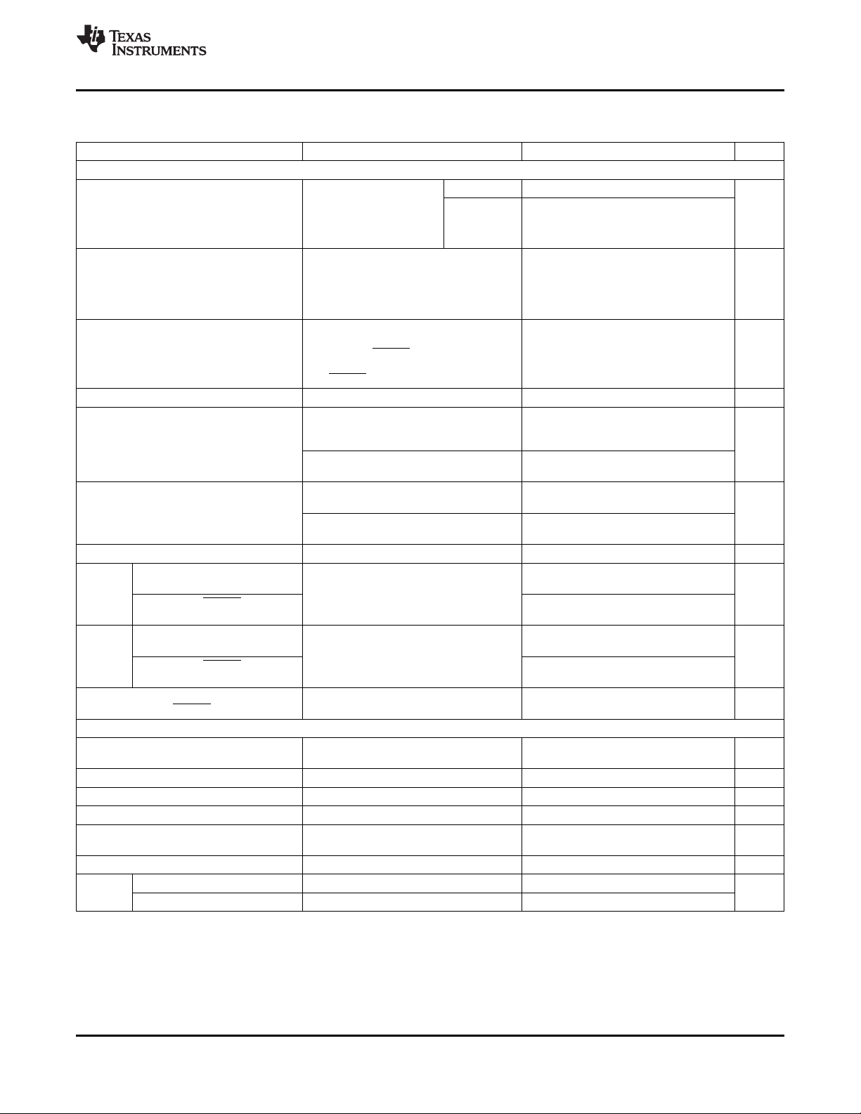
PARAMETER MEASUREMENT INFORMATION
Figure 1. Input Circuit Figure 2. Output Circuit
Figure 3. Wired OR Figure 4. LDO Output Circuit
www.ti.com
8 Submit Documentation Feedback Copyright © 2009–2010, Texas Instruments Incorporated
Product Folder Link(s) :CDC3S04
Page 9

RESET
CLKx
CLKxon Time
90%ofFinal Amplitude
REQx
CLKx
CLKxon Time
90%ofFinal Amplitude
100 sm 200 sm 300 sm 400 sm 500 sm 600 sm 700 sm 800 sm 900 sm
CLKx
VDD_ANA
CLKx on Time
90% of Final Amplitude
90% of 1.7 V
www.ti.com
CDC3S04
SCAS883A –OCTOBER 2009–REVISED JULY 2010
TYPICAL CHARACTERISTICS
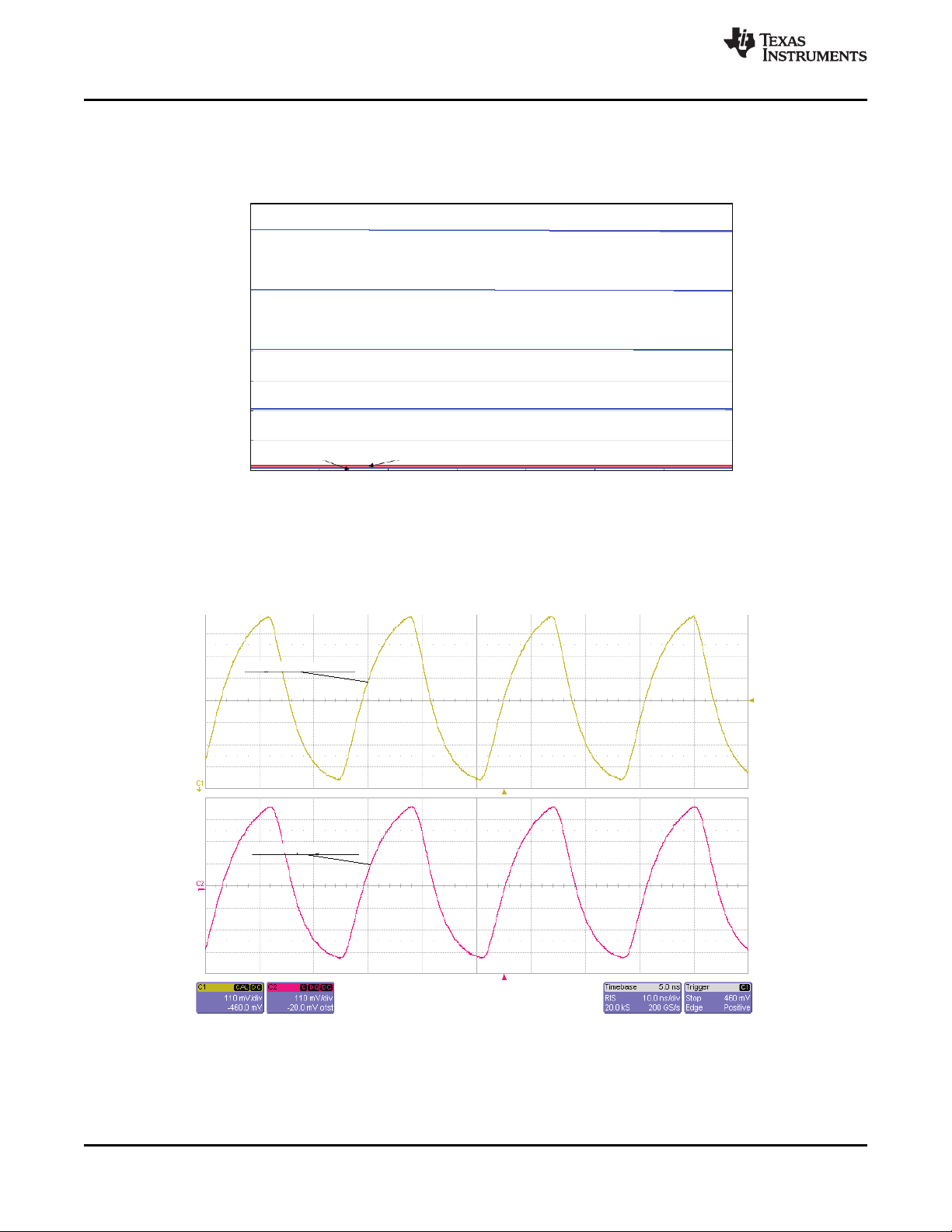
Figure 5. CLKx On-Time From RESET Off-to-On
Figure 6. CLKx On-Time From REQ Off-to-On
Copyright © 2009–2010, Texas Instruments Incorporated Submit Documentation Feedback 9
Figure 7. CLKx On-Time From V
Product Folder Link(s) :CDC3S04
DD_ANA
Off-to-On
Page 10

10
SupplyCurrent – mA
9
8
7
6
5
4
3
2
1
0
0 10 15
5
20 25 30 35 40
45
50
OutputLoad – pF
IDD_ANA /CLK1&CLK2&CLK3&CLK4
IDD_ANA /CLK1&CLK2&CLK3
IDD_ANA /CLK1&CLK2
IDD_ANA /CLK1
IDD_ANA /CLKxoff
IDD_DIG
10
SupplyCurrent – mA
9
8
7
6
5
4
3
2
1
0
0 10 15
5
20 25 30 35 40
45
50
OutputLoad – pF
IDD_ANA /CLK1&CLK2&CLK3&CLK4
IDD_ANA /CLK1&CLK2&CLK3
IDD_ANA /CLK1&CLK2
IDD_ANA /CLK1
IDD_ANA /CLKxoff
IDD_DIG
CDC3S04
SCAS883A –OCTOBER 2009–REVISED JULY 2010
TYPICAL CHARACTERISTICS (continued)
www.ti.com
SUPPLY CURRENT (IDD_ANA, IDD_DIG)
vs
OUTPUT LOAD (CL) AT 38.4 MHz INPUT CLOCK
Figure 8.
SUPPLY CURRENT (IDD_ANA, IDD_DIG)
vs
OUTPUT LOAD (CL) AT 26 MHz INPUT CLOCK
Figure 9.
10 Submit Documentation Feedback Copyright © 2009–2010, Texas Instruments Incorporated
Product Folder Link(s) :CDC3S04
Page 11

SupplyCurrent – mA
9
8
7
6
5
4
3
2
1
0
0
1
10
100
InputFrequency – MHz
IDD_ANA /CLK1&CLK2&CLK3&CLK4
IDD_ANA /CLK1&CLK2&CLK3
IDD_ANA /CLK1&CLK2
IDD_ANA /CLK1
IDD_ANA /CLKxoff IDD_DIG
SupplyCurrent – mA
9
8
7
6
5
4
3
2
1
0
0.5 0.6 0.7 0.8 0.9 1.0 1.1 1.2
InputVoltageLevel – V
PP
IDD_ANA /CLK1&CLK2&CLK3&CLK4
IDD_ANA /CLK1&CLK2&CLK3
IDD_ANA /CLK1&CLK2
IDD_ANA /CLK1
IDD_ANA /CLKxoff IDD_DIG
www.ti.com
CDC3S04
SCAS883A –OCTOBER 2009–REVISED JULY 2010
TYPICAL CHARACTERISTICS (continued)
SUPPLY CURRENT (IDD_ANA, IDD_DIG)
vs
INPUT FREQUENCY (MCLK_IN)
Figure 10.
SUPPLY CURRENT (IDD_ANA, IDD_DIG)
INPUT VOLTAGE LEVEL AT 38.4 MHz INPUT CLOCK
Copyright © 2009–2010, Texas Instruments Incorporated Submit Documentation Feedback 11
Product Folder Link(s) :CDC3S04
Figure 11.
vs
Page 12
SupplyCurrent – mA
9
8
7
6
5
4
3
2
1
0
0.5 0.6 0.7 0.8 0.9 1.0 1.1 1.2
InputVoltageLevel – V
PP
IDD_ANA /CLK1&CLK2&CLK3&CLK4
IDD_ANA /CLK1&CLK2&CLK3
IDD_ANA /CLK1&CLK2
IDD_ANA /CLK1
IDD_ANA /CLKxoff IDD_DIG
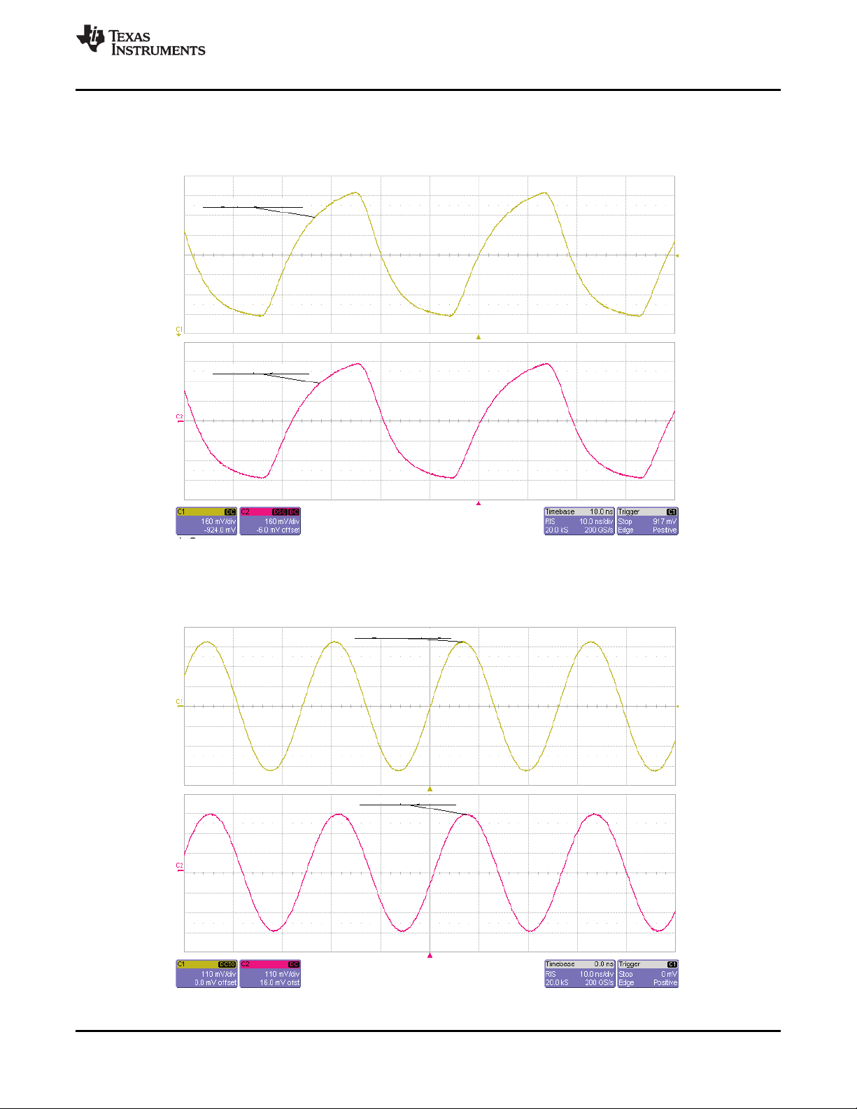
MCLK_INinputsignalfrom TCXO
CDC3S04outputsignalatCLKx
CDC3S04
SCAS883A –OCTOBER 2009–REVISED JULY 2010
TYPICAL CHARACTERISTICS (continued)
www.ti.com
SUPPLY CURRENT (IDD_ANA, IDD_DIG)
vs
INPUT VOLTAGE LEVEL AT 26 MHz INPUT CLOCK
Figure 12.
TCXO INPUT CLOCK
vs
OUTPUT CLOCK AT 38.4 MHz
Figure 13.
12 Submit Documentation Feedback Copyright © 2009–2010, Texas Instruments Incorporated
Product Folder Link(s) :CDC3S04
Page 13
MCLK_INinputsignalfrom TCXO
CDC3S04outputsignalatCLKx
MCLK_INsinusoidalinputsignal
CDC3S04outputsignalatCLKx
www.ti.com
CDC3S04
SCAS883A –OCTOBER 2009–REVISED JULY 2010
TYPICAL CHARACTERISTICS (continued)
TCXO INPUT CLOCK
vs
OUTPUT CLOCK AT 26 MHz
Figure 14.
SINE WAVE INPUT CLOCK
vs
OUTPUT CLOCK AT 38.4 MHz
Figure 15.
Copyright © 2009–2010, Texas Instruments Incorporated Submit Documentation Feedback 13
Product Folder Link(s) :CDC3S04
Page 14

MCLK_INsinusoidalinputsignal
CDC3S04outputsignalatCLKx
–7
–6
–5
–4
–3
–2
-1
0
1
1k 10k 100k 1M 10M 100M
InputFrequency – Hz
OutputGain – dB
VIS=1V
V =1.8V
PP
DD_ANA
CDC3S04
SCAS883A –OCTOBER 2009–REVISED JULY 2010
TYPICAL CHARACTERISTICS (continued)
www.ti.com
SINE WAVE INPUT CLOCK
vs
OUTPUT CLOCK AT 26 MHz
Figure 16.
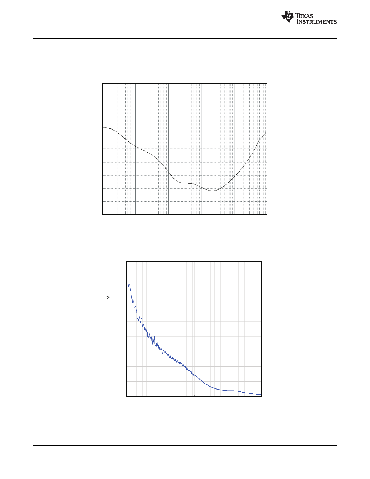
OUTPUT GAIN
vs
INPUT FREQUENCY (MCLK_IN)
14 Submit Documentation Feedback Copyright © 2009–2010, Texas Instruments Incorporated
Figure 17.
Product Folder Link(s) :CDC3S04
Page 15

CLKxOutput
MCLK_INInput
CLKxOutputHighdrive
CLKxOutput
MCLK_INInput
CLKxOutputHighdrive
www.ti.com
CDC3S04
SCAS883A –OCTOBER 2009–REVISED JULY 2010
TYPICAL CHARACTERISTICS (continued)
INPUT
vs
OUTPUT PHASE-NOISE PERFORMANCE WITH 38.4-MHz TCXO
Figure 18.
INPUT
vs
OUTPUT PHASE-NOISE PERFORMANCE WITH 26-MHz TCXO
Figure 19.
Copyright © 2009–2010, Texas Instruments Incorporated Submit Documentation Feedback 15
Product Folder Link(s) :CDC3S04
Page 16
REF50.000dB
START 100Hz 1kHz 10kHz 100kHz 1MHz STOP 10MHz
5.000dB/div
80dB
75dB
70dB
65dB
60dB
55dB
50dB
45dB
40dB
0
200
400
800
1000
1200
1400
1800
10 100 1k 10k 100k
Frequency – Hz
1600
600
SpectralNoiseDensity –
nV/Hz
CDC3S04
SCAS883A –OCTOBER 2009–REVISED JULY 2010
TYPICAL CHARACTERISTICS (continued)
www.ti.com
LDO POWER SUPPLY REJECTION
vs
FREQUENCY (PSRR)
Figure 20.
LDO OUTPUT SPECTRAL NOISE DENSITY
vs
FREQUENCY
Figure 21.
16 Submit Documentation Feedback Copyright © 2009–2010, Texas Instruments Incorporated
Product Folder Link(s) :CDC3S04
Page 17
Sr Slave Address
R/W
A A A P
Data Data
0(Write) Data Transferred
(nBytes+ Acknowledge)
FromMastertoSlave
FromSlavetoMaster
A = Acknowledge(SDAHLOW)
A = Acknowledge(SDAHHIGH)
S=START Condition
P =STOP Condition
S MasterCode
A
00001XXX
(Hs-ModeMasterCode)
F/S-Mode Hs-Mode
Sr Slave Address
R/W
A P
Data Data
1(Read) Data Transferred
(nBytes+ Acknowledge)
FromMastertoSlave
FromSlavetoMaster
A = Acknowledge(SDAHLOW)
A = Acknowledge(SDAHHIGH)
S=START Condition
P =STOP Condition
S MasterCode
A
00001XXX
(Hs-ModeMasterCode)
F/S-Mode Hs-Mode
A A
CDC3S04
www.ti.com
DETAILED DESCRIPTION
SDAH/SCLH SERIAL INTERFACE (Hs-Mode)
This section describes the SDAH/SCLH interface of the CDC3S04 device. The CDC3S04 operates as a slave
device of the two-wire serial SDAH/SCLH bus, compatible with the popular I2C specification (UM10204-I2C-bus
specification and user manual Rev. 03–19 June 2007). It operates in the high-speed mode (up to 3.4 Mbit/s) and
supports 7-bit addressing. The CDC3S04 is fully downward compatible with fast- and standard-mode (F/S)
devices for bidirectional communication in a mixed-speed bus system.
Data Protocol
The device supports byte-write and byte-read operations only. There is no block-write or block-read operation
supported; therefore, no command code byte is needed.
When a byte has been sent, it is written into the internal register and is immediately effective.
Slave Receiver Address (7 bits)
SCAS883A –OCTOBER 2009–REVISED JULY 2010
Device A6 A5 A4 A3 A2 A1 A0
CDC3S04 1 1 0 1 1 0 0 1/0
(1) Address bit A0 is selectable by the ADR_A0 input (pin D1). This allows addressing of two devices
connected to the same I2C bus. The default value is 0, set by an internal pulldown resistor.
Byte-Write Programming Sequence
Byte-Read Programming Sequence
Figure 22. Byte-Write Protocol
(1)
R/W
Copyright © 2009–2010, Texas Instruments Incorporated Submit Documentation Feedback 17
Figure 23. Byte-Read Protocol
Product Folder Link(s) :CDC3S04
Page 18

SDAH
SrSr
P
SCLH
=MCScurrent source pull-up
=Rpresistorpull-up
t
f(DA)
t
h(DAT)
t
r(CL1)
(1)
t
r(CL1)
(1)
t
r(CL)
t
su(STA)
t
(High)
t
(High)
t
su(STO)
t
r(DA)
t
h(STA)
t
su(DAT)
t
(Low)
t
(Low)
T0451-01
t
f(CL)
C
BUSCBUS
R
p
R
p
SDAH
SCLH
Master
CDC3S04
Slave
CDC3S04
SCAS883A –OCTOBER 2009–REVISED JULY 2010
(1) First rising edge of the SCLH signal after Sr and after each acknowledge bit.
Figure 24. Definition of Timing for a Complete Hs-Mode Transfer
www.ti.com
The following diagram shows how the CDC3S04 clock buffer is connected to the SDAH/SCLH serial interface
bus. Multiple devices can be connected to the bus, but the speed may need to be reduced (3.4 MHz is the
maximum) if many devices are connected.
Note that the pullup resistors (RP) depend on the supply voltage, bus capacitance, and number of connected
devices. For more details, see the I2C bus specification.
Figure 25. SDAH/SCLH Hardware Interface
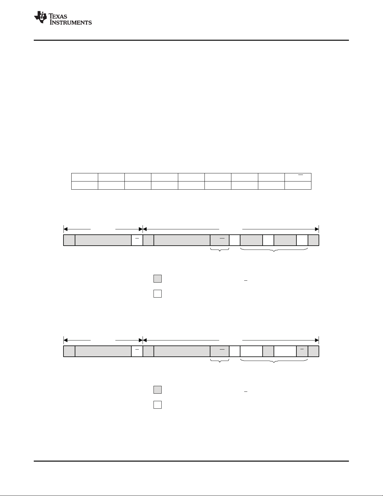
SDAH/SCLH Configuration Registers
The output stages are user configurable. Table 3 explains the programmable functions of the CDC3S04.
18 Submit Documentation Feedback Copyright © 2009–2010, Texas Instruments Incorporated
Product Folder Link(s) :CDC3S04
Page 19

www.ti.com
SCAS883A –OCTOBER 2009–REVISED JULY 2010
Table 3. Configuration Register (Shaded Cells Marks Power-Up/Default Setting)
Offset BIT
00h R/W
01h R/W
02h R/W
03h 5 HIGHDRIVE2 0h – Enables high-drive capability CLK2 Typical High R/W
(5)
04h–Bh
(1)
7 REQ4INT 1h 1h CLK4 off/on
6 REQ3INT 0h – CLK3 off/on
5 REQ2INT 0h – CLK2 off/on
4 REQ1INT 1h 1h CLK1 off/on
3 REQ4POL 1h – Selects polarity of REQ4 Active-low Active-high
2 REQ3POL 1h – Selects polarity of REQ3 Active-low Active-high
1 REQ2POL 1h – Selects polarity of REQ2 Active-low Active-high
0 REQ1POL 1h – Selects polarity of REQ1 Active-low Active-high
7 MREQ4 1h –
6 MREQ3 1h –
5 MREQ2 1h –
4 MREQ1 1h –
3 MCLKOUT1 Selects MCLK_REQ output type
2 MCLKOUT0
0–1 – 0h – Reserved
7 MREQCTRL1 MCLK_REQ generation (see Figure 27)
6 MREQCTRL0
5 LDOEN1 Switches LDO on or off:
4 LDOEN0
3 REQ4PRIO 1h 1h Defines external vs internal REQ4 priority REQ4 REQ4INT
2 REQ3PRIO 0h – Defines external vs internal REQ3 priority REQ3 REQ3INT
1 REQ2PRIO 0h – Defines external vs internal REQ2 priority REQ2 REQ2INT
0 REQ1PRIO 1h 1h Defines external vs internal REQ1 priority REQ1 REQ1INT
7 HIGHDRIVE4 0h – Enables high-drive capability CLK4 Typical High
6 HIGHDRIVE3 0h – Enables high-drive capability CLK3 Typical High
4 HIGHDRIVE1 0h – Enables high-drive capability CLK1 Typical High
0–3 – 0h – Reserved
Acronym Default
– – Reserved R/W
(1) All data is transferred with the MSB first.
(2) A device reset to default condition is initiated by a V
(3) "–" means that dedicated bits do not change at RESET.
(4) Inactive as long as the REQxPRIO bit is low, external REQx pins are valid (see Figure 26)
(5) Writing data beyond 03h may affect device function.
(2)
RESET
0h –
0h –
0h –
(3)
Description 0 1 Type
Defines if REQ4 is used to decode
MCLK_REQ
Defines if REQ3 is used to decode
MCLK_REQ
Defines if REQ2 is used to decode
MCLK_REQ
Defines if REQ1 is used to decode
MCLK_REQ
00 = wired-OR (default setting)
01 = wired-AND
1x = push-pull
0x = decoder controlled (default setting)
10 = low
11 = high
00 = LDO is on (default setting)
01 = LDO is off
1x = decoder controlled (see Figure 27)
power-up sequence.
DD_DIG
(4)
(4)
(4)
(4)
Off On
Off On
Off On
Off On
Not used for Used for
decoding decoding
CDC3S04
Copyright © 2009–2010, Texas Instruments Incorporated Submit Documentation Feedback 19
Product Folder Link(s) :CDC3S04
Page 20

signalfrom externelpin
internalsignalsor
bits from configurationregister
REQ1
REQ1POL
REQ1
REQ1INT
REQ1PRIO
XNOR
CLK1
enabled
0
1
REQ2
REQ2POL
REQ2
REQ2INT
REQ2PRIO
XNOR
0
1
REQ3
REQ3POL
REQ3
REQ3INT
REQ3PRIO
XNOR
0
1
REQ4
REQ4POL
REQ4
REQ4INT
REQ4PRIO
XNOR
CLK4
enabled
0
1
‘1’
‘1’
‘x’
‘x’
‘1’
‘1’
active-high
active-high
active-high
active-high
‘1’
‘1’
CLK2
enabledifREQ2=’1'
disabledifREQ2=’0'
CLK3
enabledifREQ3=’1'
disabledifREQ3=’0'
0
REQ1
REQ1POL
REQ2
REQ2POL
REQ3
REQ3POL
REQ4
REQ4POL
MREQ1
MREQ2
REQ1
MREQ3
MREQ4
LDOEN0
OR
REQ1INT
REQ1PRIO
REQ2
REQ2INT
REQ2PRIO
REQ3
REQ3INT
REQ3PRIO
REQ4
REQ4INT
REQ4PRIO
XNOR
XNOR
MCLK_REQ
0
1
1
0
1
LDOEN1
MREQ
CTRL0
1
MREQCTRL1
LDO is
enabled
‘0’
‘1’
‘1
‘1’
‘1’
‘1’
‘1’
‘1’
‘1’
‘x’
‘x’
‘1’
‘1’
signalfrom/to
externelpin
internalsignalsor
bits from configurationregister
active-high
‘1’
active-high
‘1’
active-high
active-high
AND
’
0
AND
AND
AND
1
0
0
1
XNOR
XNOR
CDC3S04
SCAS883A –OCTOBER 2009–REVISED JULY 2010
Figure 26. Clock Output Enable Signal
(Shaded Line Marks Power-Up/Default Setting)
www.ti.com
Figure 27. Decoding Scheme for MCLK_REQ and LDOEN
(Shaded Line Marks Power-Up/Default Setting)
20 Submit Documentation Feedback Copyright © 2009–2010, Texas Instruments Incorporated
Product Folder Link(s) :CDC3S04
Page 21

VDD_ANA
VBAT
MCLK_IN
VLDO
REQ1
CLK1
REQ2
CLK2
REQ3
CLK3
VDD_DIG
MCLK_REQ
GND_ANA
GND_DIG
RESET
REQ4
CLK4
I C(Hs-mode)
2
Peripheral 1
Peripheral 2
Peripheral 3
Peripheral 4
TCXO
38.4MHz
Battery
LDO
www.ti.com
CDC3S04
SCAS883A –OCTOBER 2009–REVISED JULY 2010
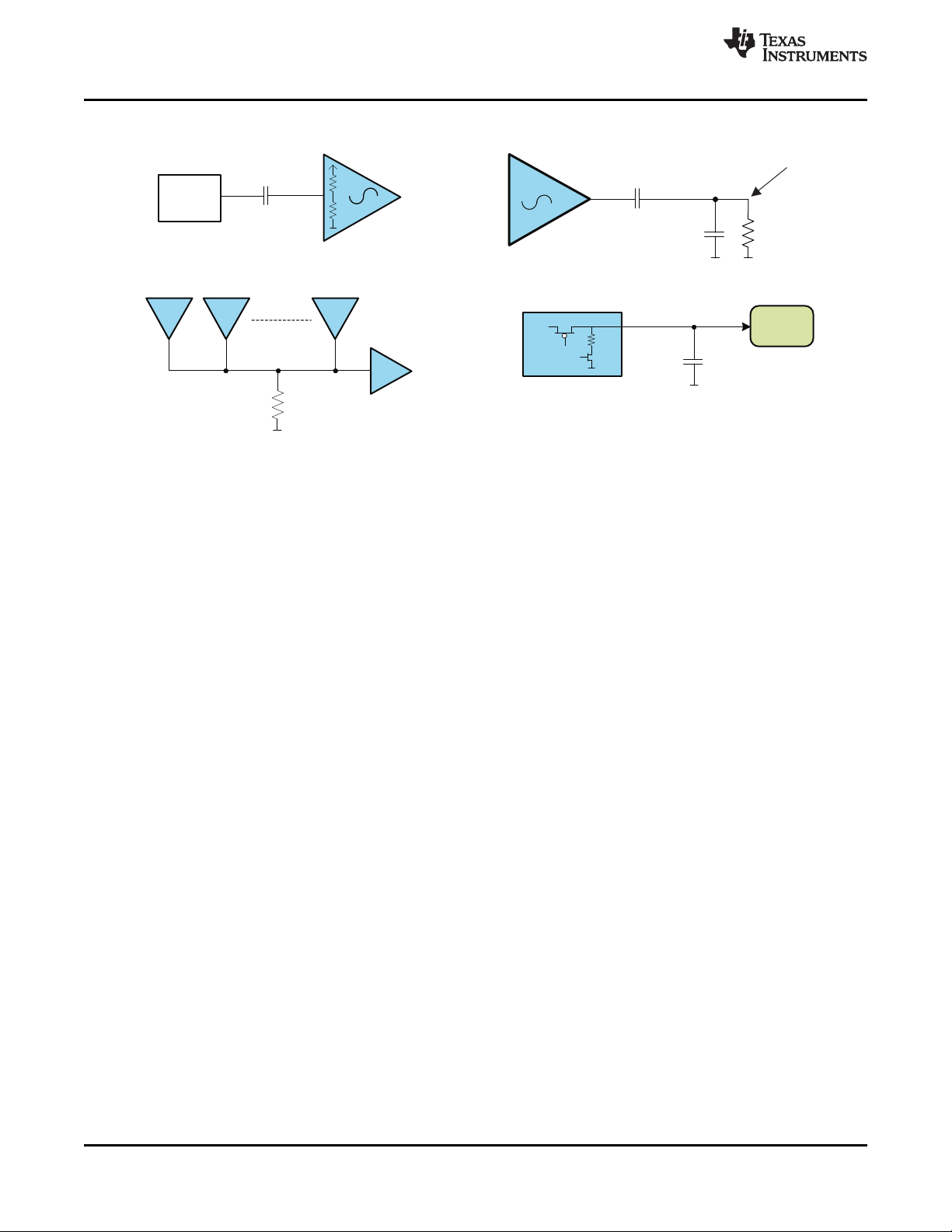
APPLICATION INFORMATION
Figure 28. Clock Distribution Scheme
Copyright © 2009–2010, Texas Instruments Incorporated Submit Documentation Feedback 21
Product Folder Link(s) :CDC3S04
Page 22

CDC3S04
SCAS883A –OCTOBER 2009–REVISED JULY 2010
REVISION HISTORY
Changes from Original (October 2009) to Revision A Page
• Changed the format on page 1 (moved 2 paragraphs from page 2 to page 1) .................................................................... 1
• Changed the X axis from 0.1us to 100us....900us ............................................................................................................... 9
• Changed Offset 00h Bit 4 Default value from 0h to 1h ....................................................................................................... 19
www.ti.com
22 Submit Documentation Feedback Copyright © 2009–2010, Texas Instruments Incorporated
Product Folder Link(s) :CDC3S04
Page 23

PACKAGE OPTION ADDENDUM
www.ti.com
17-Jul-2010
PACKAGING INFORMATION
Orderable Device
CDC3S04YFFR ACTIVE DSBGA YFF 20 3000 Green (RoHS
(1)
The marketing status values are defined as follows:
ACTIVE: Product device recommended for new designs.
LIFEBUY: TI has announced that the device will be discontinued, and a lifetime-buy period is in effect.
NRND: Not recommended for new designs. Device is in production to support existing customers, but TI does not recommend using this part in a new design.
PREVIEW: Device has been announced but is not in production. Samples may or may not be available.
OBSOLETE: TI has discontinued the production of the device.
Status
(1)
Package Type Package
Drawing
Pins Package Qty
Eco Plan
& no Sb/Br)
(2)
Lead/
Ball Finish
SNAGCU Level-1-260C-UNLIM Request Free Samples
MSL Peak Temp
(3)
Samples
(Requires Login)
(2)
Eco Plan - The planned eco-friendly classification: Pb-Free (RoHS), Pb-Free (RoHS Exempt), or Green (RoHS & no Sb/Br) - please check http://www.ti.com/productcontent for the latest availability
information and additional product content details.
TBD: The Pb-Free/Green conversion plan has not been defined.
Pb-Free (RoHS): TI's terms "Lead-Free" or "Pb-Free" mean semiconductor products that are compatible with the current RoHS requirements for all 6 substances, including the requirement that
lead not exceed 0.1% by weight in homogeneous materials. Where designed to be soldered at high temperatures, TI Pb-Free products are suitable for use in specified lead-free processes.
Pb-Free (RoHS Exempt): This component has a RoHS exemption for either 1) lead-based flip-chip solder bumps used between the die and package, or 2) lead-based die adhesive used between
the die and leadframe. The component is otherwise considered Pb-Free (RoHS compatible) as defined above.
Green (RoHS & no Sb/Br): TI defines "Green" to mean Pb-Free (RoHS compatible), and free of Bromine (Br) and Antimony (Sb) based flame retardants (Br or Sb do not exceed 0.1% by weight
in homogeneous material)
(3)
MSL, Peak Temp. -- The Moisture Sensitivity Level rating according to the JEDEC industry standard classifications, and peak solder temperature.
Important Information and Disclaimer:The information provided on this page represents TI's knowledge and belief as of the date that it is provided. TI bases its knowledge and belief on information
provided by third parties, and makes no representation or warranty as to the accuracy of such information. Efforts are underway to better integrate information from third parties. TI has taken and
continues to take reasonable steps to provide representative and accurate information but may not have conducted destructive testing or chemical analysis on incoming materials and chemicals.
TI and TI suppliers consider certain information to be proprietary, and thus CAS numbers and other limited information may not be available for release.
In no event shall TI's liability arising out of such information exceed the total purchase price of the TI part(s) at issue in this document sold by TI to Customer on an annual basis.
Addendum-Page 1
Page 24

D: Max =
1990 µm, Min =
1930 µm
E: Max =
1590 µm, Min =
1530 µm
Page 25

IMPORTANT NOTICE
Texas Instruments Incorporated and its subsidiaries (TI) reserve the right to make corrections, modifications, enhancements, improvements,
and other changes to its products and services at any time and to discontinue any product or service without notice. Customers should
obtain the latest relevant information before placing orders and should verify that such information is current and complete. All products are
sold subject to TI’s terms and conditions of sale supplied at the time of order acknowledgment.
TI warrants performance of its hardware products to the specifications applicable at the time of sale in accordance with TI’s standard
warranty. Testing and other quality control techniques are used to the extent TI deems necessary to support this warranty. Except where
mandated by government requirements, testing of all parameters of each product is not necessarily performed.
TI assumes no liability for applications assistance or customer product design. Customers are responsible for their products and
applications using TI components. To minimize the risks associated with customer products and applications, customers should provide
adequate design and operating safeguards.
TI does not warrant or represent that any license, either express or implied, is granted under any TI patent right, copyright, mask work right,
or other TI intellectual property right relating to any combination, machine, or process in which TI products or services are used. Information
published by TI regarding third-party products or services does not constitute a license from TI to use such products or services or a
warranty or endorsement thereof. Use of such information may require a license from a third party under the patents or other intellectual
property of the third party, or a license from TI under the patents or other intellectual property of TI.
Reproduction of TI information in TI data books or data sheets is permissible only if reproduction is without alteration and is accompanied
by all associated warranties, conditions, limitations, and notices. Reproduction of this information with alteration is an unfair and deceptive
business practice. TI is not responsible or liable for such altered documentation. Information of third parties may be subject to additional
restrictions.
Resale of TI products or services with statements different from or beyond the parameters stated by TI for that product or service voids all
express and any implied warranties for the associated TI product or service and is an unfair and deceptive business practice. TI is not
responsible or liable for any such statements.
TI products are not authorized for use in safety-critical applications (such as life support) where a failure of the TI product would reasonably
be expected to cause severe personal injury or death, unless officers of the parties have executed an agreement specifically governing
such use. Buyers represent that they have all necessary expertise in the safety and regulatory ramifications of their applications, and
acknowledge and agree that they are solely responsible for all legal, regulatory and safety-related requirements concerning their products
and any use of TI products in such safety-critical applications, notwithstanding any applications-related information or support that may be
provided by TI. Further, Buyers must fully indemnify TI and its representatives against any damages arising out of the use of TI products in
such safety-critical applications.
TI products are neither designed nor intended for use in military/aerospace applications or environments unless the TI products are
specifically designated by TI as military-grade or "enhanced plastic." Only products designated by TI as military-grade meet military
specifications. Buyers acknowledge and agree that any such use of TI products which TI has not designated as military-grade is solely at
the Buyer's risk, and that they are solely responsible for compliance with all legal and regulatory requirements in connection with such use.
TI products are neither designed nor intended for use in automotive applications or environments unless the specific TI products are
designated by TI as compliant with ISO/TS 16949 requirements. Buyers acknowledge and agree that, if they use any non-designated
products in automotive applications, TI will not be responsible for any failure to meet such requirements.
Following are URLs where you can obtain information on other Texas Instruments products and application solutions:
Products Applications
Amplifiers amplifier.ti.com Audio www.ti.com/audio
Data Converters dataconverter.ti.com Automotive www.ti.com/automotive
DLP® Products www.dlp.com Communications and www.ti.com/communications
DSP dsp.ti.com Computers and www.ti.com/computers
Clocks and Timers www.ti.com/clocks Consumer Electronics www.ti.com/consumer-apps
Interface interface.ti.com Energy www.ti.com/energy
Logic logic.ti.com Industrial www.ti.com/industrial
Power Mgmt power.ti.com Medical www.ti.com/medical
Microcontrollers microcontroller.ti.com Security www.ti.com/security
RFID www.ti-rfid.com Space, Avionics & www.ti.com/space-avionics-defense
RF/IF and ZigBee® Solutions www.ti.com/lprf Video and Imaging www.ti.com/video
Mailing Address: Texas Instruments, Post Office Box 655303, Dallas, Texas 75265
Copyright © 2010, Texas Instruments Incorporated
Telecom
Peripherals
Defense
Wireless www.ti.com/wireless-apps
 Loading...