

Page 1

November ’00 Preface
Series 2000 Reader System
Mini-RFM RI-RFM-003B
Reference Guide
11-06-29-030 November 2000
1
Page 2

Mini-RFM - Reference Guide November ’00
Edition Three - November 2000
This is the third edition of this manual, it describes the following equipment:
TIRIS Mini-Radio Frequency Module
Texas Instruments (TI) reserves the right to make changes to its products or services
or to discontinue any p roduc t o r se rvi ce at a ny ti me with out not ic e. T I prov id es cu stomer assistance i n various technic al areas, but do es not have full ac cess to data
concerning the use and applications of customer's products.
Therefore, TI assumes no liability and is not responsible for customer applications or
product or software design or performance relating to systems or applications incorporating TI produ cts. In addi tion, TI assu mes no liab ility and i s not respons ible for
infringement of patents and/or any other intell ectual or industrial proper ty rights of
third parties, which may result from assistance provided by TI.
TI products are not designed, intended, authorized or warranted to be suitable for life
support applications or a ny othe r li fe cr iti ca l appl ic ati on s wh ic h cou ld inv ol v e po tential risk of death, personal injury or severe property or environmental damage.
RI-RFM-003B
The
Incorporated.
Copyright 2000 Texas Instruments Incorporated (TI)
This document may be downloaded onto a computer, stored and duplicated as nec-
essary to support the us e of the related TI products. Any othe r type of duplicatio n,
circulation or storage on data carriers in any manner not authorized by TI represents
a violation of the applicable copyright laws and shall be prosecuted.
logo and the word
TIRIS
TIRIS
2
are registered trademarks of Texas Instruments
Page 3
About This Guide
Conventions
PREFACE
Read This First
This manual describes the TIR IS Mini-Radio F requency Module (M ini-RFM), it provides the information that you will need in order to install the Mini-RFM into your RFID
system. It is generally targeted at systems integrators or value added resellers.
Regulatory, safety and warranty notices that must be followed are given in
Chapter 6.
WARNING:
A
WARNING IS USED WHERE CARE MUST BE TAKEN, OR A CERTAIN
PROCEDURE
TO
HARM
MUST BE FOLLOWED IN ORDER TO PREVENT INJURY OR
YOUR HEALTH
.
If You Need Assistance
Application Centers are located in Europe, North and S outh Amer ica, the Far E ast
and Australia to provide direct su pport. For more information, please contact your
nearest TIRIS Sales and Application Center. The contact addresses can be found on
our home page:
CAUTION:
This indicates information on conditions which must be
met, or a procedure which must be followed, which if not
heeded could cause permanent damage to the equipment
or software.
Note:
Indicates conditions which must be met, or procedures which must be
followed, to ensure proper functioning of the equipment or software.
Information:
Indicates information which makes usage of the equipment or software easier
http://www.tiris.com
3
Page 4

Mini-RFM - Reference Guide November ’00
Document Overview
Page
Chapter 1: Product Description. . . . . . . . . . . . . . . . . . . . . . . . . . . . . . . . . . . . . . 5
1.1 General............................................................................................... 6
1.2 System Overview ............................................................................... 6
1.3 Product Description................................................................. ...... ..... 6
1.4 Mechanical Construction.................................................................... 7
Chapter 2: Functional Description . . . . . . . . . . . . . . . . . . . . . . . . . . . . . . . . . . . 8
2.1 General............................................................................................... 9
2.2 Transmitter ......................................................................................... 9
2.3 Receiver ........................................................................................... 11
2.4 Antenna Circuit................................................................................. 11
Chapter 3: Connectors. . . . . . . . . . . . . . . . . . . . . . . . . . . . . . . . . . . . . . . . . . . . 13
3.1 Connector Location .......................................................................... 14
3.2 Connector ST1 ................................................................................. 15
3.3 Connector ST2 ................................................................................. 16
Chapter 4: Specifications . . . . . . . . . . . . . . . . . . . . . . . . . . . . . . . . . . . . . . . . . 17
4.1 Recommended Operating Conditions .............................................. 18
4.2 Electrical Characteristics.................................................................. 18
4.3 Timing Characteristics...................................................................... 20
4.4 Mechanical Data............................................................................... 21
Chapter 5: Installation and Use. . . . . . . . . . . . . . . . . . . . . . . . . . . . . . . . . . . . . 22
5.1 Mechanical Mounting ....................................................................... 23
5.2 Supply Voltage ................................................................................. 23
5.3 Receiver Signal Strength Output RXSS-.......................................... 25
5.4 Programming a Transponder ........................................................... 27
5.5 Antenna Requirements..................................................................... 27
5.6 Antenna Tuning................................................................................ 29
Chapter 6: Warnings, Cautions and Notices . . . . . . . . . . . . . . . . . . . . . . . . . . 31
6.1 FCC / Telecommunications Regulations.......................................... 32
6.2 Important Note to Purchasers/Users of the Mini-RFM in the USA ... 32
6.3 Warning............................................................................................ 32
6.4 Cautions ........................................................................................... 32
List of Figures
Figure 1: The RI-RFM-003B........................................................................... 6
Figure 2: Mini-RFM Block Diagram.............................................................. 10
Figure 3: Mini-RFM’s Antenna Circuit .......................................................... 12
Figure 4: Top View....................................................................................... 14
Figure 5: Bottom View.................................................................................. 14
Figure 6: Maximum Supply Current I_VSP versus t_off (Power Stage)....... 19
Figure 7: Mechanical Dimensions - Top View.............................................. 21
Figure 8: Mechanical Dimensions - Side View............................................. 21
Figure 9: PCB Mounting Proposal................................................................ 23
Figure 10: Supply Line Wiring for Short Supply Lines.................................. 24
Figure 11: Supply Line Wiring for a Separated Power Supply ..................... 25
Figure 12: Synchronization output Control - Digital Adjustment................... 26
Figure 13: Synchronization output Control - Analog Adjustment ................. 26
Figure 14: Write Pulse Timing for TXCT-..................................................... 27
Figure 15: Stick Antenna RI-ANT-P02A....................................................... 28
Page
List of Tables
Table 1: Module Connector - ST1................................................................ 15
Table 2: Antenna Tuning Connector - ST2 .................................................. 16
4
Page
Page 5

Chapter 1: Product Description
This chapter introduces you to the Mini-RFM. It tells you what the module is for, provides an overview o f the comple te system and the product itself. It also provides a
mechanical description of the construction of the Mini-RFM.
Topic Page
1.1 General..........................................................................................................6
1.2 System Overview ...................... ...... ...... ....... ...... ....................................... ...6
1.3 Product Description.....................................................................................6
1.4 Mechanical Construction ............................................................................7
CHAPTER 1
Introduction
5
Page 6
Mini-RFM - Reference Guide November ’00
1.1 General
This manual provides information about the TIRIS Mini-Radio Frequency Module RIRFM-003B. It describes the module and how to integrate it into your RFID system.
This guide should be used in conjunction with the RFM Sequence Control Reference
Manual (document number 11-06-21-049) which describes the timing and sequence
of radio communica tions between the TIRIS transponder and the radio frequency
module.
1.2 Syste m Overview
The three major parts of a TIRIS system are the transponder, antenna and reader.
When a transponder is to be read, the reader sends o ut a 134.2 kHz power pulse
lasting approximately 50 ms to the antenna. The field generated by this power pulse
is “collected” by the antenna in the transponder that is tuned to the same frequency.
This received energy is stored in a small capacitor within the transponder. When the
power pulse has finished, the transponder immediately transmits its data back to the
reader, using the energy stored within its capacitor as the power source.
1.3 Product Description
The Mini-Radio F requency Module is an integ ral part of a TIRIS system, toge ther
with a control module or unit and an antenna it is use d for wireless i dentification of
TIRIS transponders.
Main tasks of the RF module are to send an energizing signal via the antenna to initialize a TIRIS trans ponder, to demodulate the receiv ed transponder identification
signal and to write to a tran sponder. The RF mo dule delivers a digi tal data stream
and a clock signal for further processing to its control unit or module. Furthermore a
field strength dependent digital output is available for synchronization purposes.
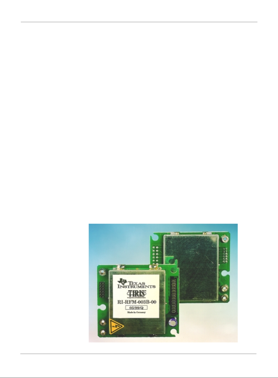
Figure 1: The RI-RFM-003B
6
Page 7

November ’00 Chapter 1. Introduction
Its small size and low supply voltag e makes the Mini-R FM well suited for portable
Reading/Writing Units, as well as for stationary equipment where medium read/write
range and speed is sufficient.
The data input and output lines are compatible with the HCMOS- logic family.
1.4 Mechanical Construction
The RF module has a simple mechanical construction where all the components are
mounted on the Printed Circuit Board (PCB). The components of the upper and lower
side of the PCB are protected by metal shields. The PCB also carries the connectors
ST1, ST2 and the antenna terminals A1 to A3 which are captive nuts soldered to the
PCB. These captive n uts allow durable low resistance connection wi th the ring terminals of the antenna.
7
Page 8

Chapter 2: Functional Description
This chapter provides an electrical description to block diagram level of how the MiniRFM works.
Topic Page
2.1 General..........................................................................................................9
2.2 Transmitter ...................................................................................................9
2.3 Receiver ......................................................................................................11
2.4 Antenna Circuit ..........................................................................................11
CHAPTER 2
Electrical Description
8
Page 9
November ’00 Chapter 2. Electrical D escription
2.1 General
The RF module is the interface between the TIRIS transponder and the data processing unit of a TIRIS Reader. It contains circuitry to:
- send a charge-up signal to a TIRIS transponder
- program a read/write transponder
- to receive the signal from the transponde r and to prepar e the recei ved signa l
for digital decoding.
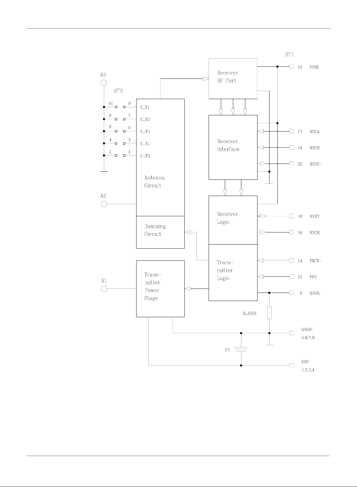
Figure 2 shows the block diagram of the RF module and unless otherwise noted the
following description refers to this schematic.
2.2 Transmitter
The transmitter control logic generates the transmitter output frequency from a
crystal-controlled oscillator. This signal is amplified by the push-pull transmitter
power stage which is connected to the antenna terminal A1. The supply current
I_VSP of the tran smitter ou tput stage d epends on t he quality factor of the antenna
being used and the supply voltage VSP. The Mini-RFM’s antenna circuit is shown in
Figure 3.
CAUTION:
Because of the necessarily low impedance of the output
stage, a short-circuit from antenna terminal A1 either to the
ground or to the supply voltage can damage the output
stage if the supply current is not limited.
The transmitter cont rol signal TXCT- activates the transmi tter as long as it is “low”.
In receive mode when TXCT- is “high” the antenna terminal A1 has a low impedance
path to the ground.
The transmitter power control signal TPC controls the intensity of the transmitter
charge pulse by changing the duty cycle of the power stage control signal. The level
of the RF power output can be reduced by setting the TPC signal to “low”. TPC controls the power setting of the RF sign al which is use d to make- up the “ powe r-bu rst” .
Both input signals TXCT- and TPC have internal pull-up resistors.
Because of the limited heatsink possibilit ies of the transmi tter power transis tors the
duty cycle of the power pulse must not be allowed to exceed that shown in Figure 6.
9
Page 10
Mini-RFM - Reference Guide November ’00
Figure 2: Mini-RFM Block Diagram
10
Page 11

November ’00 Chapter 2. Electrical D escription
2.3 Receiver
The receiver comprises three parts: the RF part, the interface and the logic.
The selective amplifier in the RF Part of the receiver:
- amplifies the RF signal received from the antenna circuit, then
- demodulates the FSK signal from the TIRIS transponder, and
- generates an analog voltage (RSSI) that provides an indication of the received
signal strength.
The demodulated FSK s ignal, carrie r signal and analo g signal stre ngth voltage ar e
all connected to the rece iv er inte r fac e. The de mod ulated data signal and the car rier
signal are conver ted to logi c si gnals , and conne cte d to th e re ceiv er logi c for fur ther
processing. The sig nal strength ind icator voltage is converted i nto RXSS- which is
fed directly to the mod ule connector ST1. The function of the RXSS- sig nal is explained in more detail in section 5.3.
The receiver logic gen erates the receiver dat a signal RXDT and the receiv er clock
signal RXCK to allow a simple data processing. The NRZ data stream of RXDT contains the identification data, the protection data and the framing bits. The clock signal
RXCK is used as time reference for the data stream of RXDT. The RXCK signal
changes from “low” to “high” level in the middle of each data bit.
2.4 Antenna Circuit
Figure 3 shows a simplified schematic of the antenna circuit. The antenna coil L_ANT
is not part of the module b ut together with the anten na circuit’s built-in c apacitors it
forms a resonanc e cir cuit. The resonant cu rren t through the antenna co il gen erates
the magnetic field which charges (and programs) the transponder.
For the system to transmit and receive correctly, the antenna must be precisely tuned
to the transmitter output frequency f_TXO to compensate for the (allowed) tolerances
of the antenna coil L_Ant and the antenna capacitors C_A1 and C_A2. To enable this
tuning, six tuning c apaci tors C_A T1 to C_AT 6 have b een added to the ante nna ci rcuit. Their values a re binary weighted in no rmalized steps of 1, 2 , 4, 8 16 and 32.
C_AT1 has the smallest value corresponding to the normalized value 1. C_AT2 has
the double capacitance of C_AT1, so that C_AT2 corresponds to the normalized value 2 and so on. With this capacitance array and six jumpers, 64 different capacitance
values can be tuned. Each of the five tuning pins has its adjacent antenna ground pin
for a simple short circuit with jumpers.
The antenna terminal A3 , which is not used in normal applicat ion s and the antenn a
ground pins of ST2 h ave same poten tial as GNDP but s hould be use d only for antenna purposes and not as a convenient ground connection.
The damping circ uit is pa rt of th e antenna circuit and dam ps the ante nna circ uit by
reducing the qual ity factor o f the built- in antenna circuit capa citor con nected to th e
terminal A2. The qua li ty fac tor is redu ce d during the receive mod e whe n th e T XCTsignal is “high”.
Information about the tuning of the antenna circuit is given in section 5.6.
11
Page 12

Mini-RFM - Reference Guide November ’00
Figure 3: Mini-RFM’s Antenna Circuit
12
Page 13

Chapter 3: Connectors
This chapter contains a listing of the module’s two connectors (ST1 and ST2) together with a list of the signals contained on each pin.
Topic Page
3.1 Connector Location...................................................................................14
CHAPTER 3
Connectors
3.2 Connector ST1............................................................................................15
3.3 Connector ST2............................................................................................16
3.4 Antenna Connector....................................................................................16
13
Page 14

Mini-RFM - Reference Guide November ’00
3.1 Connector Location
Figure 4 and Figure 5 show the location of the terminals on the PCB from the top and
from the bottom.
Figure 4: Top View
Figure 5: Bottom View
14
Page 15

November ’00 Chapter 3. Connectors
3.2 Connector ST1
Table 1: Module Connector - ST1
Pin
Number
1 VSP Supply Voltage for Power Stage (+)
2 VSP Supply Voltage for Power Stage (+)
3 VSP Supply Voltage for Power Stage (+)
4 VSP Supply Voltage for Power Stage (+)
5 GNDP Ground for Power Stage (-)
6 GNDP Ground for Power Stage (-)
7 GNDP Ground for Power Stage (-)
8 GNDP Ground for Power Stage (-)
9 GNDL Ground for Logic (-)
10 VSRL Regulated Supply voltage for Receiver and Logic (+)
11 N.C. Not connected
12 N.C. Not connected
13 N.C. Not connected
Signal
Name
Purpose
14 TXCT- Transmitter Control Input, inverted
15 TPC Transmitter Power Control Input
16 RXCK Receiver Clock Output
17 RSCA Receiver Synchronization Level Control Input, weighted 1
18 RXDT Receiver Data Output
19 RSCB Receiver Synchronization Level Control Input, weighted 2
20 RXSS- Receiver signal strength output, inverted
Important Note:
Supply terminals GNDP and GNDL must be connected externally.
15
Page 16

Mini-RFM - Reference Guide November ’00
3.3 Connector ST2
Table 2: Antenna Tuning Connector - ST2
Pin
Number
1 C_AT6 Antenna Tuning Capacitor 5, (weighted value 32)
2 GNDP Antenna Ground
3 C_AT5 Antenna Tuning Capacitor 5, (weighted value 16)
4 GNDP Antenna Ground
5 C_AT4 Antenna Tuning Capacitor 4, (weighted value 8)
6 GNDP Antenna Ground
7 C_AT3 Antenna Tuning Capacitor 3, (weighted value 4)
8 GNDP Antenna Ground
9 C_AT2 Antenna Tuning Capacitor 2, (weighted value 2)
10 GNDP Antenna Ground
11 C_AT1 Antenna Tuning Capacitor 1, (weighted value 1)
12 GNDP Antenna Ground
Signal
Name
Purpose
3.4 Antenna Connector
Table 3: Antenna Connector
Pin
Number
A1 Antenna Terminal 1
A2 Antenna Terminal 2
A3 Antenna Ground (GNDP)
Purpose
CAUTION:
Never try to connect the antenna bet ween A1 and A3, or A2
and A3; as this will damage the module.
16
Page 17

Chapter 4: Specifications
CHAPTER 4
Specifications
This chapter provides the specific details that you will need in order to use the
Mini-Radio Frequency
trical characteristics, timing characteristics and mechanical data.
Module RI-RFM-003B
correctly. It includes general data, elec-
TIRIS
Topic Page
4.1 Recommended Operating Conditions......................................................18
4.2 Electrical Characteristics..........................................................................18
4.3 Timing Characteristics ..............................................................................20
4.4 Mechanical Data.........................................................................................21
17
Page 18

Mini-RFM - Reference Guide November ’00
4.1 Recommended Operating Conditions
Operating free-air temperature range.......................... 0 to +50 °C
Storage temperature range........................................ -25 to +85 °C
Note:
Free-air temperature: air temperature immediately surrounding the
Mini-RFM. If the module is incorporated into a housing, it must be
guaranteed by proper design or cooling that the internal temperature
does not exceed the ratings given here.
Parameter Description Condition
VSRL Supply voltage for logic - 10 4.75 5.25 V
VSP
VIL
VIH
Supply voltage for
transmitter power stage
Low level input voltage for
TXCT- and TPC
High level input volt age for
TXCT- and TPC
4.2 Electrical Characteristics
at T
Parameter Description Condition
=25 °C, VSRL=5.0V (unless otherwise noted)
amb
Note:
The voltage difference between GNDL and GNDP must not exceed
0.5 V.
Pin No.
of ST1
- 1,2, 3, 4 4.5 6.0 V
VSRL=5.0 14, 15 0 1.0 V
VSRL=5.0 14, 15 4.0 5.0 V
Pin No.
of ST1
min. nom. max Unit
min. max Unit
I_VSRL Supply current for logic and receiver - 10 - - 80 mA
VSP=5V
TXCT-=”low”
TPC=”high”
VSP=5V
TXCT-=”high”
---22-kOhm
V_IL=0V 14, 15 -180 - -300 µA
V_IL=4V 14, 15 -30 - -60 µA
1,2,3,4 0.5 - 1.2 A
1,2,3,4 - - 50 µA
I_VSP
I_VSP_L
R_up
I_IL
I_IH
Supply current for transmitter power
stage with antenna Ri-ANT-P02A
Leakage current for transmitt er power
stage with antenna Ri-ANT-P02A
Pull-up resistor from TXCT- and TPC
to VRSL
Low level input current for TCXT- and
TPC
High level input current for TCXTand TPC
18
Page 19

November ’00 Chapter 4. Specifications
Parameter Description Condition
I_IL
I_IH
V_OH
V_OH
V_OL
R_GND
Parameter Description Condition
C_A1
+C_A2
C_AT6 Antenna tuning capacity weighted 32 - 1 1425 1500 1575 pF
C_AT5 Antenna tuning capacity weighted 16 - 3 740 780 820 pF
C_AT4 Antenna tuning capacity weighted 8 - 5 370 391 410 pF
C_AT3 Antenna tuning capacity weighted 4 - 7 209 220 231 pF
Low level input current for RS CA and
RSCB
High level input current for RSC A and
RSCB
High level output voltage for RXCK,
RXDT and RXSS-
High level output voltage for RXCK,
RXDT and RXSS-
Low level output voltage for RXCK,
RXDT and RXSS-
Decoupling resistor between GNDL
and GNDP
Antenna capacity
V_IL=0V 17, 19 - -30 µA
V_IH=5V 17, 19 - - 30 µA
I_OH=-2mA
I_OH=-1mA
I_OL=-2mA
-
without tuning
cap.
Pin No.
of ST1
16, 18,
20
16, 18,
20
16, 18,
20
9 to
5,6,7,8
Pin No.
of ST2
A2 10.6 - 11.8 nF
min. nom. max Unit
2,4--V
4.0--V
--0.5V
-33-Ohm
min. nom. max Unit
C_AT2 Antenna tuning capacity weighted 2 - 9 95 100 105 pF
C_AT1 Antenna tuning capacity weighted 1 - 11 50 56 64 pF
Figure 6: Maximum Supply Current I_VSP versus t_off (Power Stage)
1.8
1.5
1.2
0.9
0.6
I_VSP_max [A]
0.3
0
0
50
(250)
Time t_off between 2 charge pulses of 50 ms [ms]
Values in brackets ( ) are for time t_off between 2 write cycles
100
(400)
150
(550)
200
(700)
250
(850)
19
Page 20

Mini-RFM - Reference Guide November ’00
4.3 Timing Characteristics
at T
=0-50 °C, VSRL=5.0 V, VSP=5.0 V
amb
Parameter Description Condition
f_TX Transmitter frequency - A1 134.1 134.2 134.3 kHz
f_OSC
f_mRX
b_RX Bandwidth of receiver - - - 22 - kHz
t_rin,
t_fin
t_rout,
t_fout
f_REPwrt
f_REPrd
Internal oscillator
frequency
Center frequency of
receiver
Rise and fall time of
the input signals
TXCT- and TPC
Rise and fall time of
the output signals
RXCK, RXDT, RXSS-
Repetition rate to
program with Antenna
= RI-ANT-P02A
Repetition rate to re ad
with Antenna =
RI-ANT-P02A
- - - 4294.4 - kHz
- - - 128.2 - kHz
- 14, 15 - - 100 ns
-
t_wrt=310ms
TPC=”high
t_charge=
50ms
TPC=”high”
Pin No.
of ST1
17, 18,
20
---1Hz
---4Hz
min. nom. max. Unit
--1µs
t_offL
t_offH
Transmitter OFF-time
for databit = “L”
Transmitter OFF-time
for databit=”H”
t_bit=2ms - - 0.5 - ms
t_bit=2ms - - 1.2 - ms
20
Page 21

November ’00 Chapter 4. Specifications
4.4 Mechanical Data
Length......................................................................... 60.2 mm
Width........................................................................... 55.1 mm
Height, body................................................................ 10.4 mm
Height, at connector.................................................... 11.5 mm
Weight......................................................................... 40 g
Figure 7 shows the top view and Figure 8 shows the side view of the RF module, both
drawings show the most important dimensions. The center of the upper right mounting hole serves as reference point for all dimensions.
Figure 7: Mechanical Dimensions - Top View
Figure 8: Mechanical Dimensions - Side View
21
Page 22

Chapter 5: Installation and Use
This chapter provides the specific details that you will need in order to install the
TIRIS Mini-RFM
quirements, the antenn a characteristics , the connecting cable and how to tune th e
antenna to resonance.
Topic Page
5.1 Mechanical Mounting.............. ...... ...... ....... ...... ....................................... .23
5.2 Supply Voltage .........................................................................................23
correctly. It includes a detailed des cription o f the power supply re-
CHAPTER 5
Installation and Use
5.3 Receiver Signal Strength Output RXSS-................................................25
5.4 Programming a Transponder..................................................................27
5.5 Antenna Requirements............................................................................27
5.6 Antenna Tuning........................................................................................29
5.6.1 To Switch-ON the Transmitter..............................................................29
5.6.2 To Tune the Antenna Circuit ................................................................29
5.6.3 To Detect the Correct Tuning...............................................................29
5.6.4 Tuning Procedure.................................................................................30
22
Page 23

November ’00 Chapter 5. Installation and Use
5.1 Mechanical Mounting
To protect the RF module from strong mechanical shock and vibration, grommets are
inserted into the mounting hole of the PCB as shown in Figure 9. Because the grommets are made of soft material, eyelets or spacers must be inserted into them when
the RF module is mounted with screws.
Figure 9: PCB Mounting Proposal
5.2 Supply Voltage
The module uses two different supply lines each with a separate ground line. The receiver and the logic are sup plied via the VS RL and GNDL pins from a voltage regulated power supply. The transmitter power stage with its relatively high current
consumption is supplie d via the VSP and GNDP pins. The su pply volt age range for
VSP is wider than for VSL. This allows the direct connection of VS P to a four cell
NiCd battery, if the variation of the power pulse field strength caused by the variation
of the battery voltage is acceptable.
Both ground lines GNDL and GNDP are decoupled inside the RFM with the resistor
R_GND and the capacitor C_GND and have to be connected together externally as
shown in Figure 10 or Figure 11 (d epending o n your power s upply ). This tec hniqu e
allows the power ground level GNDP to float in a certain range against the lo gic
ground level G NDL wi thout c reating adv erse ef fects to th e co ntrol signal s fr om an d
to the control unit. Floating GNDP c an happ en dur ing trans mit tim e if yo u are usin g
a long supply line between the RF module and a control module.
Note:
Take care when disconnecting ST1 that you pull the plug straight out
and do not apply any sideways strain to the plastic guides.
23
Page 24

Mini-RFM - Reference Guide November ’00
Figure 10 shows an ex ample of how to s upply the RF module i n a battery s upplied
reading unit where short lines are possible.
Figure 11 shows an example of how to wire a stationary application where long supply lines (over 1 5 cm) are used. The capac itor C_E1 betwee n the VSP a nd GNDP
pins is necessar y to reduce the RF ripple voltage and EMI on the supply line and
must have low impedance at the transmit frequency (ESR = Equivalent Serial Resistor). In addition the common m ode chok e coil (ch oke) and the capaci tor C_E2 als o
reduce the EMI during transmit time. These components should be placed as closely
as possible to the RF module connector ST1.
The capacitor values shown in Figure 10 and Figure 11 are for general use and can
vary according to different application requirements.
Regardless of which kind of power supply you use, we recommend that you build in
fuses or electronic current limitations in between the RF module and the power supplies to avoid any damage in case of short circuit. The value of the fuse depends very
much on the application, fo r ex am ple: the c ur rent c ons um pti on of the modu le whic h
in turn depends on severa l fact ors , such as : the an tenn a use d, whether or not a capacitor is connected and its size.
Note:
The fuse load for VSP under normal conditions is less than 1 A.
However, if the Mini-RFM is connected into an application where the
power is permanently on (hot” connecting), the load could surge by
several amps due to the current in capacitor CS1 inside the MiniRFM.
Figure 10: Supply Line Wiring for Short Supply Lines
24
Page 25

November ’00 Chapter 5. Installation and Use
Figure 11: Supply Line Wiring for a Separated Power Supply
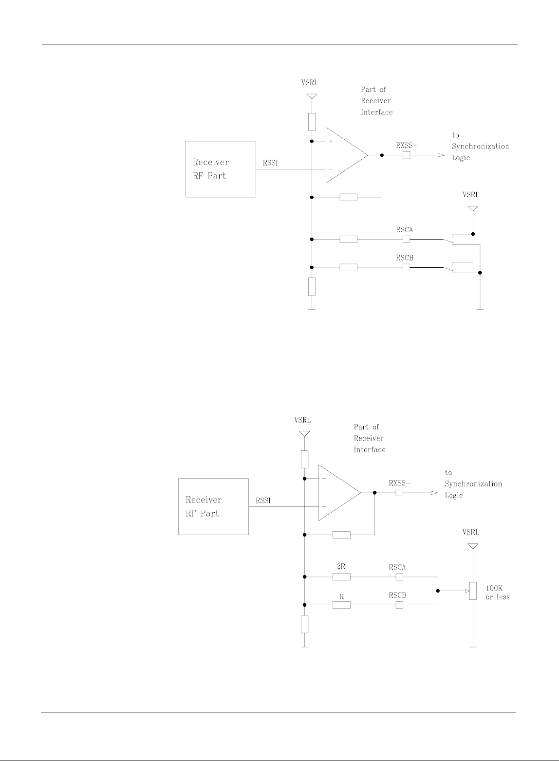
5.3 Receiver Signal Strength Output RXSS-
If you are going to operate more than one TIR IS reader in a local area, the systems
should be synchr onized to each other. An in telligent co ntrol unit a chieves this sy nchronization by sa mpling for the p resenc e or a bsence of the fi eld str ength i ndicator
signal RXSS-. A power pulse in the area will cause RXSS- to be active. If the signal
RXSS- is present the control unit ensures that the RF module transmits either simultaneously or sequentially to any other RFMs in the area.
The RXSS- output switches to “low” if the received signal strength exceeds the internal reference level. This reference level can be adjusted with the two receiver signal
strength control inputs RSCA and RSCB.
Figure 12 and Figure 13 s how the basic schemat ic of the signal strength i ndicator
and two methods of adjusting the switching level.
The circuit shown in Figure 12 works as a simple D/A converter where the digital inputs RSCA and RSCB are switched either to the ground GNDL or to the supply voltage VSRL. Because of the high inpu t imp eda nc e of RSCA and RSCB, the switches
can be replaced by computer controlled outputs. Such a circuit can adjust the sensitivities in four steps. A fifth step is given if both inputs are open.
25
Page 26
Mini-RFM - Reference Guide November ’00
Figure 12: Synchronization output Control - Digital Adjustment
An analog adjust ment of the sensitivity le vel can be realized if a pote ntiometer is
used as shown in Figure 13 or if a variable voltage source is used to bias one or both
of the control inputs RSCA and RSCB.
Figure 13: Synchronization output Control - Analog Adjustment
26
Page 27

November ’00 Chapter 5. Installation and Use
5.4 Programming a Transponder
To write data to a read/write transp onder the transmi tter of the RF modul e must be
switched off and on periodically after the power pulse is completed. As shown in Figure 14 each data bit has the same length t_bit, but the duration t_offL or t_offH during
which the transmitter is switched off, determines the value of the bit. Because the antenna circuit of the module and the connected antenna form a resonance circuit with
a specific rise and fall char acteristic o f the resonan ce voltage, different RF mo dule
and antenna combinations might need different t_offL and t_offH timing. The values
t_offL and t_offH shown in section 4.3 'Timing Characteristics' are the times applied
to TXCT-. A high Q antenna such as RI-ANT-P02A is used.
Figure 14: Write Pulse Timing for TXCT-
A detailed descr iption of the complete programming sequence is given in the Sequence Control Manual (document number 11-06-21-049).
5.5 Antenna Requirements
The antenna for a TIRIS RF m odule i s a coi l with the inductance L_ANT and the Qfactor Q_ANT. To ensure that the antenna can be tuned to resonance with the tuning
capacitors inside the RF Modul e, the induc tance L_ANT f or an air c oil ante nna ca n
vary in the limits given below:
L_ANT = 115 to 117 µH (at f=134.2 kHz, V=1V)
Q_ANT = 200 or better is recommended for good read/write range.
Some factors which often influence each other, are listed below.
a. The
magnetic field strength. The larger the area of an air coil antenna or the longer a
ferrite core antenna is, the higher the field strength for a given RFM set-up and a
given Q-factor of the antenna coil.
b. The
quality depends on the construction and the wire used for the coil. Because of the
high frequency, litze-wire is needed for a high Q-factor. The higher the Q-factor of
the antenna coil the more energy can be “pulled” from the RF module for a given
RF module set-up. If an antenna with ferrite core is used, it must be kept in mind
that it may have a very high quality factor under test conditions, but the quality
factor will drop if a high magnetic field is applied to the ferrite core.
and the
size
quality factor
construction
of the antenna coil is a parameter indicating its efficiency. The
of the antenna coil is a key factor for the generated
c. A very important factor for a good read/write range is the correct
polarization
unit.
between the transponder antenna and the antenna of the read/write
27
orientation
/
Page 28

Mini-RFM - Reference Guide November ’00
d.
Figure 15 shows th e d imens io ns of th e fe rr ite s ti ck an tenna RI-ANT-P02A ava ilabl e
for the RF Module RI-RFM-003B.
Figure 15: Stick Antenna RI-ANT-P02A
, i.e. magnetic interference energy in or close to the TIRIS frequency range
Noise
can reduce the read range remarkably. Sources of interference can be, for
example: electronic equipment with built-in switch mode power supplies, monitors
and TV-sets with their magnetic deflection, which are not shielded enough. In such
conditions you may be able to obtain better read/write ranges with a smaller
antenna rather than a large one. The reason for this is that a large antenna collects
signals within a larger area and therefore produces a stronger interference signal
compared with the relatively small transponder signal. Under some conditions,
charging and/or writing to the transponder works excellently, but the reading unit
cannot detect the transponder signal.
28
Page 29

November ’00 Chapter 5. Installation and Use
5.6 Antenna Tuning
In order to get all the avai lable field strength from the antenna, it must b e tuned to
resonance. To do this, the following set-up and equipment are required.
5.6.1 To Switch-ON the Transmitter
The reading/writing unit or test set up should be able to switch the RF module’s transmitter to a fast re peating reading m ode or continuous wave mode. If a con tinuous
wave mode is applied, care must be taken not to exceed the duty cycle limitation as
given in section 4.3. Time when the tr ansmitter is swi tched on but duri ng which the
current consumption is less than I_VSPcont, does not add to the duty cycle.
5.6.2 To Tune the Antenna Circuit
The built-in tuning capacitors C_AT1 to C_AT6 which are available at ST2 should be
used to tune the resonance frequency of the antenna circuit to the output frequency
of the transmitter. The most s imple method of tuning is to use a “Swi tch Box” connected to the antenna tuning connector ST2, this will allow the capacity of the antenna resonant circuit to be increased by connecting the built-in tuning capacitors to the
ground.
The “Switch Box” in its simpl est ve rsio n is an array of six wel l isolate d, hig h voltag e
proof ON/OFF switches , whic h are con nected to the ant enna tun ing co nnecto r ST2
(Antenna Tuning Switch Box R I-ACC-ATS1).
If you have to tune a lot of Mini -R FMs ( for example on a production r un) it wo uld be
helpful to build a computer (or electronically) controlled tuning box which allows you
to start the tuning pr oc ed ure an d th en s et the jum pers according to the res ult of th e
tuning. The cable from the “switch bo x” to th e conne ctor S T2 shoul d be as s hort as
possible (less that 20 cm) in order to get the same tuning results as with the jumpers.
5.6.3 To Detect the Correct Tuning
There are two basic methods to detect the correct tuning point, they are:
One method is to tune the antenna circuit to maximum current consumption of
the transmitter power stage by inserting a current meter into the VSP-line
which is an easy way for production. The lines of the meter should be as short
as possible, or they must be RF decoupled close to the RF module.
The second method is to tune the antenna circuit to the maximum of the magnetic field strength generated by the antenn a.
29
Page 30

Mini-RFM - Reference Guide November ’00
5.6.4 Tuning Procedure
WARNING:
C
ARE MUST BE TAKEN WHEN HANDLING THE MINI
VOLTAGE
TORS COULD BE HARMFUL TO YOUR HEALTH
INSULATION
M
INI
ACROSS THE ANTENNA TERMINALS AND TUNING CONNEC
IS
DAMAGED IT MUST NOT BE CONNECTED TO THE
-RFM.
-RFM. H
. IF
THE ANTENNA
IGH
-
Ensure that the reader is switched OFF.
Connect the antenna to the RF Module.
Remove all jumper s from the tuning connec tor ST2 and connect the “Switch Box”
with all six switches in the OFF position.
Switch the RF module transmitter ON (continuous or fast reading mode).
While watching the current met er, increase tuning capacity with the “Switch Box”
step-by-step until you find a peak.
Note:
If you are using a switch box, do not forget that the capacitors
attached to the jumpers are binary weighted, and that you should set
the switches in a binary way:
Switch 1 ON
Switch 1 OFF Switch 2 ON
Switch 1 ON Switch 2 ON
Switch 1 OFF Switch 2 OFF Switch 3 ON
and so on.
When you find a pe ak cont inue with two more st ep s and c heck in c as e y ou fi nd another, higher peak. Looking for a possible second peak is necessary because the capacitors of the tuning network have overlapping capacitance, which causes
discontinuous cap ac itanc e step s.
Check if the power stage supply current or the field strength has the correct value for
that application.
Switch the transm itter OFF , disconnec t the switc h box and then plug-in jumpers at
all the places where the switches are in the ON position.
Switch ON the equipment again and check if the current or field strength are almost
the same as they were with the switch box connected.
Switch OFF the transmitter or reading unit. Tuning is completed.
30
Page 31

Warnings, Cautions and Notices
Chapter 6: Warnings, Cautions and Notices
This chapter provides th e Warnings, Cautions and Notic es that are relevant to the
Mini-RFM.
Topic Page
6.1 FCC / Telecommunications Regulations .................................................32
6.2 Important Note to Purchasers/Users of the Mini-RFM in the USA ........32
6.3 Warning.......................................................................................................32
6.4 Cautions......................................................................................................32
CHAPTER 6
31
Page 32

Mini-RFM - Reference Guide November ’00
6.1 FCC / Telecommunications Regulations
The TIRIS RF Module gene rates RF emissions at 134.2 kHz. The r adiation of the
fundamental and the harmonics will vary with the type of antenna and other devices
or functions connected to the RF module.
The required FCC or Telecommunications approvals must be obtained prior to operating the TIRIS RF Module wi th antenna(s) , power supp ly and a control modu le or
other devices.
Sale, lease or ope ration in other c ountries may be subject to prio r approval by th e
government or other organizations.
6.2 Important Note to Purchasers/Users of the Mini-RFM in the USA
The TIRIS RF Module product is co nside red by th e Fede ral Co mmuni catio ns Commission (FCC) to be a “s ubassembly ”. As suc h, no prior ap proval is required to import, sell or otherwise market the RF Module in the United States. In order to form a
functioning radio fr eq uen cy RF dev i ce , the R F M odu le mus t be co nne cte d to a su itable antenna, power supply, and control circuitry. A radio frequency device may not
be operated unless authorized by the FCC nor may a radio frequency device be marketed (i.e. sold, lea sed, imported, or a dvertised for sa le or lease) without t he prior
grant of an FCC equipment authorization.
6.3 Warning
6.4 Cautions
FCC authorization to operate an RF device may take one of two forms: first, the FCC
may grant the user an exper imental lic ense; se cond, the FCC may i ssue an equ ipment authorization pe rmitting use of th e RF device on an unli censed basis. TI ca n
assist the user in obtaining an experimental license that will cover a specific installation of the RF Module in a spe cif ic s ite or si tes . E xp erime nta l au thor iza tio ns ar e appropriate to cover o perations during the development of an RF device. A grant of
equipment authorizat ion (known as “certification ”) must be obtained from the FCC
before RF devices are marketed or operated on a nondevelopment basis.
An equipment auth orization ha s alrea dy be en is sued for use of th e RF Module and
other TIRIS equipment (including antennas) in certain configurations. This authorization does not cover all possible combinations of equipment and, in particular, covers
only specific anten na configurat ions. Shou ld a user de sire to use the RF Module in
a configuration not yet approved, TI can assist that customer to obtain the necessary
equipment approval.
Care must be taken when handling the RF Module. High voltage across the antenna
terminals and tuning co nnector could be harmful to you r he alt h. If the an tenn a ins ulation is damaged it should not be connected to the RF Module.
The RF Module m ight be subject to damage by electro static discharge (ES D) and
should therefore only be handled by ESD protected personnel at ESD secured workplaces.
32
Page 33

November ’00 Chapter 6. Warnings, Cautions and Abbreviations
The transmitter power output stage can be damaged, if the antenna terminal A1 has
a short circuit e ither to the gr ound or to th e sup ply voltag e and no c urrent limit ation
is applied.
The transmitter power o utput stage can o perate only with a limite d duty cyc le. This
subject needs to be given attention especially during the antenna tuning procedure.
The ground pins GNDL and GNDP have to be connected externally to avoid damage
to the RF Module.
33
Page 34

Mini-RFM - Reference Guide November ’00
34
 Loading...