

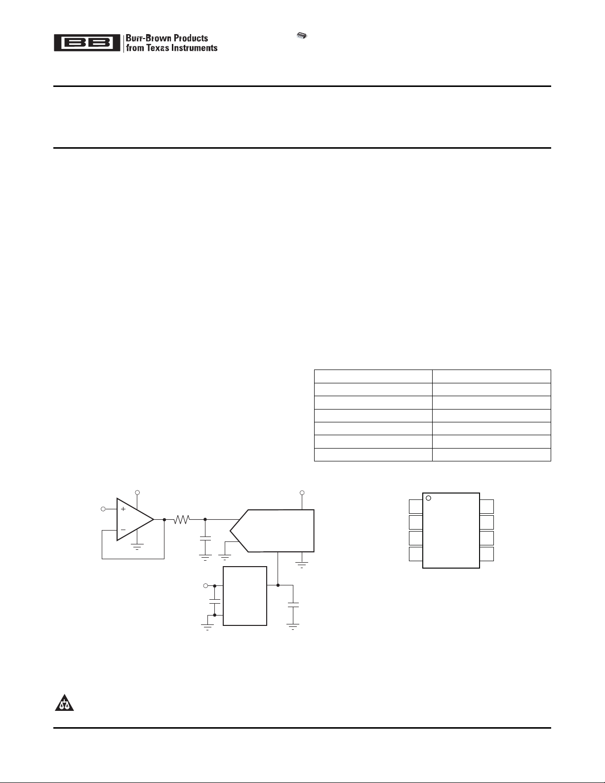
ADS8326
REF5040
REF
V
OUT
GND
+IN
-IN
V
IN
+5V
OPA365
Input
Signal
0Vto4V
+5V
+5V
V
DD
GND
C
BYPASS
1 Fm
R
1
50W
C
1
1.2nF
C
2
22 Fm
1
2
3
4
8
7
6
5
DNC
(1)
NC
(2)
TRIM
DNC
(1)
V
IN
TEMP
GND
V
OUT
REF50xx
SO-8,MSOP-8
(3)
(1)DNC=Donotconnect.
(2)NC=Nointernalconnection.
(3)MSOP-8packageavailableQ3,2007.
NOTES:
www.ti.com
Low-Noise, Very Low Drift, Precision
VOLTAGE REFERENCE
1
FEATURES
2
• LOW TEMPERATURE DRIFT:
– High-Grade: 3ppm/ ° C (max)
– Standard-Grade: 8ppm/ ° C (max)
• HIGH ACCURACY:
– High-Grade: 0.05% (max)
– Standard-Grade: 0.1% (max)
• LOW NOISE: 3 μ V
• HIGH OUTPUT CURRENT: ± 10mA
• TEMPERATURE RANGE: – 40 ° C to +125 ° C
APPLICATIONS
• 16-BIT DATA ACQUISITION SYSTEMS
• ATE EQUIPMENT
• INDUSTRIAL PROCESS CONTROL
• MEDICAL INSTRUMENTATION
• OPTICAL CONTROL SYSTEMS
• PRECISION INSTRUMENTATION
/V
PP
REF5020 , , REF5025
REF5030 , REF5040
REF5045 , REF5050
SBOS410 – JUNE 2007
DESCRIPTION
The REF50xx is a family of low-noise, low-drift, very
high precision voltage references. These references
are capable of both sinking and sourcing, and are
very robust with regard to line and load changes.
Excellent temperature drift (3ppm/ ° C) and high
accuracy (0.05%) are achieved using proprietary
design techniques. These features, combined with
very-low noise make the REF50xx family ideal for use
in high-precision data acquisition systems.
Each reference voltage is available in both standardand high-grade versions. They are offered in MSOP-8
(available Q3, 2007) and SO-8 packages, and are
specified from – 40 ° C to +125 ° C.
REF50xx Family
MODEL OUTPUT VOLTAGE
REF5020 2.048V
REF5025 2.5V
REF5030 3.0V
REF5040 4.096V
REF5045 4.5V
REF5050 5.0V
1
Please be aware that an important notice concerning availability, standard warranty, and use in critical applications of
Texas Instruments semiconductor products and disclaimers thereto appears at the end of this data sheet.
2 All trademarks are the property of their respective owners.
PRODUCTION DATA information is current as of publication date.
Products conform to specifications per the terms of the Texas
Instruments standard warranty. Production processing does not
necessarily include testing of all parameters.
Copyright © 2007, Texas Instruments Incorporated
www.ti.com
REF5020 , , REF5025
REF5030 , REF5040
REF5045 , REF5050
SBOS410 – JUNE 2007
This integrated circuit can be damaged by ESD. Texas Instruments recommends that all integrated circuits be handled with
appropriate precautions. Failure to observe proper handling and installation procedures can cause damage.
ESD damage can range from subtle performance degradation to complete device failure. Precision integrated circuits may be more
susceptible to damage because very small parametric changes could cause the device not to meet its published specifications.
PACKAGE/ORDERING INFORMATION
PRODUCT OUTPUT VOLTAGE PACKAGE-LEAD PACKAGE DESIGNATOR PACKAGE MARKING
STANDARD GRADE (8ppm, 0.1%)
REF5020A 2.048V
REF5025A 2.5V
REF5030A 3.0V
REF5040A 4.096V
REF5045A 4.5V
REF5050A 5.0V
HIGH GRADE (3ppm, 0.05%)
REF5020I 2.048V
REF5025I 2.5V
REF5030I 3.0V
REF5040I 4.096V
REF5045I 4.5V
REF5050I 5.0V
SO-8 D REF5020
(2)
MSOP-8
SO-8 D REF5025
(2)
MSOP-8
SO-8 D REF5030
(2)
MSOP-8
SO-8 D REF5040
(2)
MSOP-8
SO-8 D REF5045
(2)
MSOP-8
SO-8 D REF5050
(2)
MSOP-8
SO-8 D REF5020
(2)
MSOP-8
SO-8 D REF5025
(2)
MSOP-8
SO-8 D REF5030
(2)
MSOP-8
SO-8 D REF5040
(2)
MSOP-8
SO-8 D REF5045
(2)
MSOP-8
SO-8 D REF5050
(2)
MSOP-8
(1)
DGK R50A
DGK R50B
DGK R50C
DGK R50D
DGK R50E
DGK R50F
DGK R50A
DGK R50B
DGK R50C
DGK R50D
DGK R50E
DGK R50F
(1) For the most current package and ordering information see the Package Option Addendum at the end of this document, or see the TI
web site at www.ti.com .
(2) MSOP-8 (DGK) package available Q3, 2007.
ABSOLUTE MAXIMUM RATINGS
(1)
PARAMETER REF50xx UNIT
Input Voltage +18 V
Output Short-Circuit 30 mA
Operating Temperature Range – 55 to +125 ° C
Storage Temperature Range – 55 to +150 ° C
Junction Temperature (T
ESD Rating
max) +150 ° C
J
Human Body Model (HBM) 3000 V
Charged Device Model (CDM) 1000 V
(1) Stresses above these ratings may cause permanent damage. Exposure to absolute maximum conditions for extended periods may
degrade device reliability. These are stress ratings only, and functional operation of the device at these or any other conditions beyond
those specified is not implied.
2
Copyright © 2007, Texas Instruments Incorporated
Submit Documentation Feedback
Product Folder Link(s): REF5020 REF5025 REF5030 REF5040 REF5045 REF5050
www.ti.com
REF5020 , , REF5025
REF5030 , REF5040
REF5045 , REF5050
SBOS410 – JUNE 2007
ELECTRICAL CHARACTERISTICS: PER DEVICE
Boldface limits apply over the specified temperature range, TA= – 40 ° C to +125 ° C.
At TA= +25 ° C, I
OUTPUT VOLTAGE
Output Voltage V
Initial Accuracy: High-Grade – 0.05 0.05 %
NOISE
Output Voltage Noise f = 0.1Hz to 10Hz 6 μ V
OUTPUT VOLTAGE
Output Voltage V
Initial Accuracy: High-Grade – 0.05 0.05 %
NOISE
Output Voltage Noise f = 0.1Hz to 10Hz 7.5 μ V
OUTPUT VOLTAGE
Output Voltage V
Initial Accuracy: High-Grade – 0.05 0.05 %
NOISE
Output Voltage Noise f = 0.1Hz to 10Hz 9 μ V
OUTPUT VOLTAGE
Output Voltage V
Initial Accuracy: High-Grade – 0.05 0.05 %
NOISE
Output Voltage Noise f = 0.1Hz to 10Hz 12 μ V
OUTPUT VOLTAGE
Output Voltage V
Initial Accuracy: High-Grade – 0.05 0.05 %
NOISE
Output Voltage Noise f = 0.1Hz to 10Hz 13.5 μ V
OUTPUT VOLTAGE
Output Voltage V
Initial Accuracy: High-Grade – 0.05 0.05 %
NOISE
Output Voltage Noise f = 0.1Hz to 10Hz 15 μ V
(1) For V
≤ 2.5V, the minimum supply voltage is 2.7V.
OUT
= 0, CL= 1 μ F, and V
LOAD
= (V
IN
+ 0.2V) to 18V, unless otherwise noted.
OUT
PER DEVICE
PARAMETER CONDITIONS MIN TYP MAX UNIT
REF5020 (V
OUT
= 2.048V)
OUT
2.7V < VIN< 18V 2.048 V
(1)
Standard-Grade – 0.1 0.1 %
REF5025 (V
OUT
= 2.5V)
OUT
2.5 V
Standard-Grade – 0.1 0.1 %
REF5030 (V
OUT
= 3.0V)
OUT
3.0 V
Standard-Grade – 0.1 0.1 %
REF5040 (V
OUT
= 4.096V)
OUT
4.096 V
Standard-Grade – 0.1 0.1 %
REF5045 (V
OUT
= 4.5V)
OUT
4.5 V
Standard-Grade – 0.1 0.1 %
REF5050 (V
OUT
= 5.0V)
OUT
5.0 V
Standard-Grade – 0.1 0.1 %
PP
PP
PP
PP
PP
PP
Copyright © 2007, Texas Instruments Incorporated
3
Submit Documentation Feedback
Product Folder Link(s): REF5020 REF5025 REF5030 REF5040 REF5045 REF5050
www.ti.com
REF5020 , , REF5025
REF5030 , REF5040
REF5045 , REF5050
SBOS410 – JUNE 2007
ELECTRICAL CHARACTERISTICS: ALL DEVICES
Boldface limits apply over the specified temperature range, TA= – 40 ° C to +125 ° C.
At TA= +25 ° C, I
OUTPUT VOLTAGE TEMPERATURE DRIFT
Output Voltage Temperature Drift dV
High-Grade 2.5 3 ppm/ ° C
Standard-Grade 3 8 ppm/ ° C
LINE REGULATION
Line Regulation dV
REF5020
All Other Devices 0.1 1 ppm/V
Over Temperature 0.2 1 ppm/V
LOAD REGULATION
Load Regulation dV
Over Temperature 50 ppm/mA
SHORT-CIRCUIT CURRENT
Short-Circuit Current I
TEMP PIN
Voltage Output At TA= +25 ° C 575 mV
Temperature Sensitivity 2.64 mV/ ° C
TURN-ON SETTLING TIME
Turn-On Settling Time To 0.1% with CL= 1 μ F 200 μ s
POWER SUPPLY
Supply Voltage V
Quiescent Current 0.8 1 mA
Over Temperature 1.2 mA
TEMPERATURE RANGE
Specified Range – 40 +125 ° C
Operating Range – 55 +125 ° C
Thermal Resistance θ
MSOP-8 150 ° C/W
SO-8 150 ° C/W
(1) For V
(1)
Only VIN= 2.7V to 18V 0.1 1 ppm/V
≤ 2.5V, the minimal supply voltage is 2.7V.
OUT
= 0, CL= 1 μ F, and V
LOAD
PARAMETER CONDITIONS MIN TYP MAX UNIT
= (V
IN
/dT
OUT
/dV
OUT
IN
/d
OUT
ILOAD
SC
S
JA
+ 0.2V) to 18V, unless otherwise noted.
OUT
– 10mA < I
< +10mA, VIN= V
LOAD
See Note
V
= 0 25 mA
OUT
REF50xx
+ 0.75V 20 30 ppm/mA
OUT
(1)
V
(1)
+ 0.2
OUT
18 V
4
Copyright © 2007, Texas Instruments Incorporated
Submit Documentation Feedback
Product Folder Link(s): REF5020 REF5025 REF5030 REF5040 REF5045 REF5050
www.ti.com
0
0.25
0.50
0.75
1.00
1.25
1.50
1.75
2.00
2.25
2.50
2.75
3.00
3.25
3.50
3.75
4.00
4.25
4.50
4.75
5.00
Drift(ppm/ C)°
P
opulation(%)
0
0.50
1.00
1.50
2.00
2.50
3.00
3.50
4.00
4.50
5.00
5.50
6.00
6.50
7.00
7.50
8.00
Drift(ppm/ C)°
Population(%)
-50 -25
Temperature( C)°
0.05
0.04
0.03
0.02
0.01
0
-0.01
-0.02
-0.03
-0.04
-0.05
OutputVoltageAccuracy(%)
1250 25 50 75 100
-0.05
-0.04
-
0.03
-0.02
-0.01
0
0.01
0.02
0.03
0.04
0.05
Drift(ppm/ C)°
Population(%)
10
Frequency(Hz)
160
140
120
100
80
60
40
20
0
PSRR(dB)
100k100 1k 10k
-15 -10 -5
LoadCurrent(mA)
0.8
0.7
0.6
0.5
0.4
0.3
0.2
0.1
0
DropoutVoltage(V)
150 5 10
+125 C°
+25 C°
- °40 C
At TA= +25 ° C, I
TYPICAL CHARACTERISTICS
= 0, and VS= V
LOAD
TEMPERATURE DRIFT TEMPERATURE DRIFT
(0 ° C to +85 ° C) ( – 40 ° C to +125 ° C)
Figure 1. Figure 2.
+ 0.2V, unless otherwise noted. For V
OUT
OUT
REF5020 , , REF5025
REF5030 , REF5040
REF5045 , REF5050
SBOS410 – JUNE 2007
≤ 2.5V, the minimum supply voltage is 2.7V.
OUTPUT VOLTAGE OUTPUT VOLTAGE ACCURACY
INITIAL ACCURACY vs TEMPERATURE
Figure 3. Figure 4.
POWER-SUPPLY REJECTION RATIO
vs FREQUENCY DROPOUT VOLTAGE vs LOAD CURRENT
Copyright © 2007, Texas Instruments Incorporated
Figure 5. Figure 6.
Submit Documentation Feedback
Product Folder Link(s): REF5020 REF5025 REF5030 REF5040 REF5045 REF5050
5

www.ti.com
-10 -5
LoadCurrent(mA)
2.50125
2.50100
2.50075
2.50050
2.50025
2.50000
2.49975
2.49950
2.49925
2.49900
2.49875
OutputVoltage(V)
100 5
+125 C°
+25 C°
- °40 C
-50 -25
Temperature( C)°
0.9
0.8
0.7
0.6
0.5
0.4
0.3
TEMPPinOutputVoltage(V)
1250 25 50 75 100
-50 -25
Temperature( C)°
1050
1000
950
900
850
800
750
700
650
600
QuiescentCurrent(mA)
1250 25 50 75 100
-50 -25
Temperature( C)°
0.5
0.4
0.3
0.2
0.1
0
-0.1
-0.2
-0.3
-0.4
-0.5
LineRegulation(ppm/V)
1250 25 50 75 100
1s/div
1 V/divm
-50 -25
Temperature( C)°
35
30
25
20
15
10
5
0
Short-CircuitCurrent(mA)
1250 25 50 75 100
Sourcing
Sinking
REF5020 , , REF5025
REF5030 , REF5040
REF5045 , REF5050
SBOS410 – JUNE 2007
At TA= +25 ° C, I
TYPICAL CHARACTERISTICS (continued)
= 0, and VS= V
LOAD
REF5025 OUTPUT VOLTAGE TEMP PIN OUTPUT VOLTAGE
vs LOAD CURRENT vs TEMPERATURE
Figure 7. Figure 8.
+ 0.2V, unless otherwise noted. For V
OUT
OUT
≤ 2.5V, the minimum supply voltage is 2.7V.
QUIESCENT CURRENT LINE REGULATION
vs TEMPERATURE vs TEMPERATURE
Figure 9. Figure 10.
SHORT-CIRCUIT CURRENT
vs TEMPERATURE NOISE
6
Figure 11. Figure 12.
Submit Documentation Feedback
Product Folder Link(s): REF5020 REF5025 REF5030 REF5040 REF5045 REF5050
Copyright © 2007, Texas Instruments Incorporated

www.ti.com
40 s/divm
2V/div
1V/div
V
OUT
V
IN
400 s/divm
5V/div
1V/div
V
OUT
V
IN
20 s/divm
-1mA
-1mA
+1mA
I
LOAD
V
OUT
5mV/div
1mA/div
20 s/divm
-10mA
+10mA+10mA
I
LOAD
V
OUT
2mV/div
10mA/div
100 s/divm
-1mA
-1mA
+1mA
I
LOAD
V
OUT
5mV/div
1mA/div
100 s/divm
-10mA
-10mA
+10mA
I
LOAD
V
OUT
2mV/div
10mA/div
At TA= +25 ° C, I
= 0, and VS= V
LOAD
TYPICAL CHARACTERISTICS (continued)
+ 0.2V, unless otherwise noted. For V
OUT
STARTUP STARTUP
(REF5025, CL= 1 μ F) (REF5025, CL= 10 μ F)
Figure 13. Figure 14.
LOAD TRANSIENT LOAD TRANSIENT
(C
= 1 μ F, I
L
= 1mA) (C
OUT
≤ 2.5V, the minimum supply voltage is 2.7V.
OUT
= 1 μ F, I
L
OUT
REF5020 , , REF5025
REF5030 , REF5040
REF5045 , REF5050
SBOS410 – JUNE 2007
= 10mA)
Copyright © 2007, Texas Instruments Incorporated
Figure 15. Figure 16.
LOAD TRANSIENT LOAD TRANSIENT
(C
= 10 μ F, I
L
= 1mA) (C
OUT
Figure 17. Figure 18.
Submit Documentation Feedback
Product Folder Link(s): REF5020 REF5025 REF5030 REF5040 REF5045 REF5050
= 10 μ F, I
L
= 10mA)
OUT
7

www.ti.com
20ms/div
V
OUT
V
IN
5mV/div
500mV/div
100 s/divm
V
OUT
V
IN
5mV/div
500mV/div
REF5020 , , REF5025
REF5030 , REF5040
REF5045 , REF5050
SBOS410 – JUNE 2007
At TA= +25 ° C, I
= 0, and VS= V
LOAD
TYPICAL CHARACTERISTICS (continued)
+ 0.2V, unless otherwise noted. For V
OUT
LINE TRANSIENT LINE TRANSIENT
(C
= 1 μ F) (C
L
Figure 19. Figure 20.
≤ 2.5V, the minimum supply voltage is 2.7V.
OUT
= 10 μ F)
L
8
Copyright © 2007, Texas Instruments Incorporated
Submit Documentation Feedback
Product Folder Link(s): REF5020 REF5025 REF5030 REF5040 REF5045 REF5050

www.ti.com
1.2V
60kW
REF50xx
TEMP
V
OUT
V
IN
GND
TRIM
Bandgap
+V
SUPPLY
µT
µT
(10 Am
at25 C)°
DNC
TEMP
V
OUT
V
IN
GND
DNC
NC
TRIM
REF50xx
+V
SUPPLY
10kW
1kW
470W
DNC
TEMP
V
OUT
V
IN
GND
DNC
NC
TRIM
REF50xx
C
BYPASS
1 Fto10 Fm m
C
L
1 Fto50 Fm m
+V
SUPPLY
V
OUT
Drift +
ǒ
V
OUTMAX
* V
OUTMIN
V
OUT
Temp Range
Ǔ
106(ppm)
REF5020 , , REF5025
REF5030 , REF5040
REF5045 , REF5050
SBOS410 – JUNE 2007
APPLICATION INFORMATION
The REF50xx is family of low-noise, precision
bandgap voltage references that are specifically
designed for excellent initial voltage accuracy and
drift. Figure 21 shows a simplified block diagram of
the REF50xx.
SUPPLY VOLTAGE
The REF50xx family of voltage references features
extremely low dropout voltage. With the exception of
the REF5020, which has a minimum supply
requirement of 2.7V, these references can be
operated with a supply of 200mV above the output
voltage in an unloaded condition. For loaded
conditions, a typical dropout voltage versus load plot
is shown in Figure 6 of the Typical Characteristics.
OUTPUT ADJUSTMENT (TRIM Pin)
The REF50xx provides a very accurate voltage
output. However, V
nominal value for the purpose of trimming system
errors by configuring the TRIM pin (pin 5). The TRIM
pin provides for adjustment of the voltage at V
over a ± 15mV range. Figure 23 shows a typical circuit
using the TRIM pin to adjust V
technique, the temperature coefficients of the
resistors can degrade the temperature drift at the
output.
can be adjusted from the
OUT
. When using this
OUT
OUT
Figure 21. REF50xx Simplified Block Diagram
BASIC CONNECTIONS
Figure 22 shows the typical connections for the
REF50xx. A supply bypass capacitor ranging
between 1 μ F to 10 μ F is recommended. A 1 μ F to
50 μ F, low-ESR output capacitor (C
connected to V
Copyright © 2007, Texas Instruments Incorporated
Figure 22. Basic Connections
.
OUT
Product Folder Link(s): REF5020 REF5025 REF5030 REF5040 REF5045 REF5050
) must be
L
Submit Documentation Feedback
Figure 23. V
Adjustment Using the TRIM Pin
OUT
TEMPERATURE DRIFT
The REF50xx is designed for minimal drift error,
which is defined as the change in output voltage over
temperature. The drift is calculated using the box
method, as described by the following equation:
The REF50xx features a maximum drift coefficient of
3ppm/ ° C for the high-grade version, and 8ppm/ ° C for
the standard-grade.
(1)
9

www.ti.com
DNC
TEMP
V
OUT
V
IN
GND
DNC
NC
TRIM
REF50xx
V
TEMP
2.6mV/ C°
OPA
(1)
NOTE:(1)Lowdriftopamp,suchastheOPA333,OPA335,orOPA376.
+V
REF5020 , , REF5025
REF5030 , REF5040
REF5045 , REF5050
SBOS410 – JUNE 2007
TEMPERATURE MONITORING POWER DISSIPATION
The temperature output terminal (TEMP, pin 3) The REF50xx family is specified to deliver current
provides a temperature-dependent voltage output loads of ± 10mA over the specified input voltage
with approximately 60k Ω source impedance. As seen range. The temperature of the device increases
in Figure 8 , the output voltage follows the nominal according to the equation:
relationship:
V
TEMP PIN
= 509mV + 2.64 × T( ° C)
This pin indicates general chip temperature, accurate
to approximately ± 15 ° C. Although it is not generally
suitable for accurate temperature measurements, it
can be used to indicate temperature changes or for
temperature compensation of analog circuitry. A
temperature change of 30 ° C corresponds to an
approximate 79mV change in voltage at the TEMP
pin.
The TEMP pin has high output impedance (see
Figure 21 ). Loading this pin with a low-impedance
circuit induces a measurement error; however, it does
not have any effect on V
OUT
accuracy. To avoid
errors caused by low-impedance loading, buffer the
TEMP pin output with a suitable low-temperature drift
op amp, such as the OPA333 , OPA335 , or OPA376 ,
as shown in Figure 24 .
TJ= TA+ PD× θ
JA
Where:
TJ= Junction temperature ( ° C)
TA= Ambient temperature ( ° C)
P
= Power dissipated (W)
D
θ
= Junction-to-ambient thermal resistance
JA
( ° C/W)
The REF50xx junction temperature must not exceed
the absolute maximum rating of +150 ° C.
NOISE PERFORMANCE
Typical 0.1Hz to 10Hz voltage noise for each member
of the REF50xx family is specified in the Electrical
Characteristics: Per Device table. The noise voltage
increases with output voltage and operating
temperature. Additional filtering can be used to
improve output noise levels, although care should be
taken to ensure the output impedance does not
degrade performance.
Figure 24. Buffering the TEMP Pin Output
10
Product Folder Link(s): REF5020 REF5025 REF5030 REF5040 REF5045 REF5050
Copyright © 2007, Texas Instruments Incorporated
Submit Documentation Feedback

www.ti.com
APPLICATION CIRCUITS
ADS8326
REF5040
REF
V
OUT
GND
+IN
-IN
V
IN
+5V
OPA365
Input
Signal
0Vto4V
+5V
+5V
V
DD
GND
C
BYPASS
1 Fm
R
1
50W
C
1
1.2nF
C
2
22 Fm
-2.5V
+2.5V
+5V
NOTE:Bypasscapacitorsnotshown.
R
1
10kW
R
2
10kW
-5V
OPA735
+5V
DNC
TEMP
V
OUT
V
IN
GND
DNC
NC
TRIM
REF5025
1 Fm
REF5020 , , REF5025
REF5030 , REF5040
REF5045 , REF5050
SBOS410 – JUNE 2007
NEGATIVE REFERENCE VOLTAGE
For applications requiring a negative and positive
reference voltage, the REF50xx and OPA735 can be
used to provide a dual-supply reference from a 5V
supply. Figure 25 shows the REF5025 used to
provide a 2.5V supply reference voltage. The low drift
performance of the REF50xx complements the low
offset voltage and zero drift of the OPA735 to provide
an accurate solution for split-supply applications.
Care must be taken to match the temperature
coefficients of R
and R2.
1
DATA ACQUISITION
Data acquisition systems often require stable voltage
references to maintain accuracy. The REF50xx family
features low noise, very low drift, and high initial
accuracy for high-performance data converters.
Figure 26 shows the REF5040 in a basic data
acquisition system.
Figure 26. Basic Data Acquisition System
Figure 25. The REF5025 and OPA735 Create
Positive and Negative Reference Voltages
Copyright © 2007, Texas Instruments Incorporated
Product Folder Link(s): REF5020 REF5025 REF5030 REF5040 REF5045 REF5050
Submit Documentation Feedback
11
PACKAGE OPTION ADDENDUM
www.ti.com
PACKAGING INFORMATION
Orderable Device Status
REF5020AID ACTIVE SOIC D 8 75 Green (RoHS &
REF5020AIDG4 ACTIVE SOIC D 8 75 Green (RoHS &
REF5020AIDR ACTIVE SOIC D 8 2500 Green (RoHS &
REF5020AIDRG4 ACTIVE SOIC D 8 2500 Green (RoHS &
REF5020ID ACTIVE SOIC D 8 75 Green (RoHS &
REF5020IDG4 ACTIVE SOIC D 8 75 Green (RoHS &
REF5020IDR ACTIVE SOIC D 8 2500 Green (RoHS &
REF5020IDRG4 ACTIVE SOIC D 8 2500 Green (RoHS &
REF5025AID ACTIVE SOIC D 8 75 Green (RoHS &
REF5025AIDG4 ACTIVE SOIC D 8 75 Green (RoHS &
REF5025AIDR ACTIVE SOIC D 8 2500 Green (RoHS &
REF5025AIDRG4 ACTIVE SOIC D 8 2500 Green (RoHS &
REF5025ID ACTIVE SOIC D 8 75 Green (RoHS &
REF5025IDG4 ACTIVE SOIC D 8 75 Green (RoHS &
REF5025IDR ACTIVE SOIC D 8 2500 Green (RoHS &
REF5025IDRG4 ACTIVE SOIC D 8 2500 Green (RoHS &
REF5030AID ACTIVE SOIC D 8 75 Green (RoHS &
REF5030AIDG4 ACTIVE SOIC D 8 75 Green (RoHS &
REF5030AIDR ACTIVE SOIC D 8 2500 Green (RoHS &
REF5030AIDRG4 ACTIVE SOIC D 8 2500 Green (RoHS &
REF5030ID ACTIVE SOIC D 8 75 Green (RoHS &
REF5030IDG4 ACTIVE SOIC D 8 75 Green (RoHS &
REF5030IDR ACTIVE SOIC D 8 2500 Green (RoHS &
REF5030IDRG4 ACTIVE SOIC D 8 2500 Green (RoHS &
REF5040AID ACTIVE SOIC D 8 75 Green (RoHS &
(1)
Package
Type
Package
Drawing
Pins Package
Qty
Eco Plan
no Sb/Br)
no Sb/Br)
no Sb/Br)
no Sb/Br)
no Sb/Br)
no Sb/Br)
no Sb/Br)
no Sb/Br)
no Sb/Br)
no Sb/Br)
no Sb/Br)
no Sb/Br)
no Sb/Br)
no Sb/Br)
no Sb/Br)
no Sb/Br)
no Sb/Br)
no Sb/Br)
no Sb/Br)
no Sb/Br)
no Sb/Br)
no Sb/Br)
no Sb/Br)
no Sb/Br)
no Sb/Br)
(2)
Lead/Ball Finish MSL PeakTemp
CU NIPDAU Level-2-260C-1 YEAR
CU NIPDAU Level-2-260C-1 YEAR
CU NIPDAU Level-2-260C-1 YEAR
CU NIPDAU Level-2-260C-1 YEAR
CU NIPDAU Level-2-260C-1 YEAR
CU NIPDAU Level-2-260C-1 YEAR
CU NIPDAU Level-2-260C-1 YEAR
CU NIPDAU Level-2-260C-1 YEAR
CU NIPDAU Level-2-260C-1 YEAR
CU NIPDAU Level-2-260C-1 YEAR
CU NIPDAU Level-2-260C-1 YEAR
CU NIPDAU Level-2-260C-1 YEAR
CU NIPDAU Level-2-260C-1 YEAR
CU NIPDAU Level-2-260C-1 YEAR
CU NIPDAU Level-2-260C-1 YEAR
CU NIPDAU Level-2-260C-1 YEAR
CU NIPDAU Level-2-260C-1 YEAR
CU NIPDAU Level-2-260C-1 YEAR
CU NIPDAU Level-2-260C-1 YEAR
CU NIPDAU Level-2-260C-1 YEAR
CU NIPDAU Level-2-260C-1 YEAR
CU NIPDAU Level-2-260C-1 YEAR
CU NIPDAU Level-2-260C-1 YEAR
CU NIPDAU Level-2-260C-1 YEAR
CU NIPDAU Level-2-260C-1 YEAR
23-Jul-2007
(3)
Addendum-Page 1

PACKAGE OPTION ADDENDUM
www.ti.com
Orderable Device Status
(1)
Package
Type
Package
Drawing
Pins Package
Qty
Eco Plan
REF5040AIDG4 ACTIVE SOIC D 8 75 Green (RoHS &
(2)
Lead/Ball Finish MSL Peak Temp
CU NIPDAU Level-2-260C-1 YEAR
23-Jul-2007
(3)
no Sb/Br)
REF5040AIDR ACTIVE SOIC D 8 2500 Green (RoHS &
CU NIPDAU Level-2-260C-1 YEAR
no Sb/Br)
REF5040AIDRG4 ACTIVE SOIC D 8 2500 Green (RoHS &
CU NIPDAU Level-2-260C-1 YEAR
no Sb/Br)
REF5040ID ACTIVE SOIC D 8 75 Green (RoHS &
CU NIPDAU Level-2-260C-1 YEAR
no Sb/Br)
REF5040IDG4 ACTIVE SOIC D 8 75 Green (RoHS &
CU NIPDAU Level-2-260C-1 YEAR
no Sb/Br)
REF5040IDR ACTIVE SOIC D 8 2500 Green (RoHS &
CU NIPDAU Level-2-260C-1 YEAR
no Sb/Br)
REF5040IDRG4 ACTIVE SOIC D 8 2500 Green (RoHS &
CU NIPDAU Level-2-260C-1 YEAR
no Sb/Br)
REF5045AID ACTIVE SOIC D 8 75 Green (RoHS &
CU NIPDAU Level-2-260C-1 YEAR
no Sb/Br)
REF5045AIDG4 ACTIVE SOIC D 8 75 Green (RoHS &
CU NIPDAU Level-2-260C-1 YEAR
no Sb/Br)
REF5045AIDR ACTIVE SOIC D 8 2500 Green (RoHS &
CU NIPDAU Level-2-260C-1 YEAR
no Sb/Br)
REF5045AIDRG4 ACTIVE SOIC D 8 2500 Green (RoHS &
CU NIPDAU Level-2-260C-1 YEAR
no Sb/Br)
REF5045ID ACTIVE SOIC D 8 75 Green (RoHS &
CU NIPDAU Level-2-260C-1 YEAR
no Sb/Br)
REF5045IDG4 ACTIVE SOIC D 8 75 Green (RoHS &
CU NIPDAU Level-2-260C-1 YEAR
no Sb/Br)
REF5045IDR ACTIVE SOIC D 8 2500 Green (RoHS &
CU NIPDAU Level-2-260C-1 YEAR
no Sb/Br)
REF5045IDRG4 ACTIVE SOIC D 8 2500 Green (RoHS &
CU NIPDAU Level-2-260C-1 YEAR
no Sb/Br)
REF5050AID ACTIVE SOIC D 8 75 Green (RoHS &
CU NIPDAU Level-2-260C-1 YEAR
no Sb/Br)
REF5050AIDG4 ACTIVE SOIC D 8 75 Green (RoHS &
CU NIPDAU Level-2-260C-1 YEAR
no Sb/Br)
REF5050AIDR ACTIVE SOIC D 8 2500 Green (RoHS &
CU NIPDAU Level-2-260C-1 YEAR
no Sb/Br)
REF5050AIDRG4 ACTIVE SOIC D 8 2500 Green (RoHS &
CU NIPDAU Level-2-260C-1 YEAR
no Sb/Br)
REF5050ID ACTIVE SOIC D 8 75 Green (RoHS &
CU NIPDAU Level-2-260C-1 YEAR
no Sb/Br)
REF5050IDG4 ACTIVE SOIC D 8 75 Green (RoHS &
CU NIPDAU Level-2-260C-1 YEAR
no Sb/Br)
REF5050IDR ACTIVE SOIC D 8 2500 Green (RoHS &
CU NIPDAU Level-2-260C-1 YEAR
no Sb/Br)
REF5050IDRG4 ACTIVE SOIC D 8 2500 Green (RoHS &
CU NIPDAU Level-2-260C-1 YEAR
no Sb/Br)
(1)
The marketing status values are defined as follows:
ACTIVE: Product device recommended for new designs.
LIFEBUY: TI has announced that the device will be discontinued, and a lifetime-buy period is in effect.
NRND: Not recommended for new designs. Device is in production to support existing customers, but TI does not recommend using this part in
a new design.
PREVIEW: Device has been announced but is not in production. Samples may or may not be available.
Addendum-Page 2

PACKAGE OPTION ADDENDUM
www.ti.com
OBSOLETE: TI has discontinued the production of the device.
(2)
Eco Plan - The planned eco-friendly classification: Pb-Free (RoHS), Pb-Free (RoHS Exempt), or Green (RoHS & no Sb/Br) - please check
http://www.ti.com/productcontent for the latest availability information and additional product content details.
TBD: The Pb-Free/Green conversion plan has not been defined.
Pb-Free (RoHS): TI's terms "Lead-Free" or "Pb-Free" mean semiconductor products that are compatible with the current RoHS requirements
for all 6 substances, including the requirement that lead not exceed 0.1% by weight in homogeneous materials. Where designed to be soldered
at high temperatures, TI Pb-Free products are suitable for use in specified lead-free processes.
Pb-Free (RoHS Exempt): This component has a RoHS exemption for either 1) lead-based flip-chip solder bumps used between the die and
package, or 2) lead-based die adhesive used between the die and leadframe. The component is otherwise considered Pb-Free (RoHS
compatible) as defined above.
Green (RoHS & no Sb/Br): TI defines "Green" to mean Pb-Free (RoHS compatible), and free of Bromine (Br) and Antimony (Sb) based flame
retardants (Br or Sb do not exceed 0.1% by weight in homogeneous material)
(3)
MSL, Peak Temp. -- The Moisture Sensitivity Level rating according to the JEDEC industry standard classifications, and peak solder
temperature.
Important Information and Disclaimer:The information provided on this page represents TI's knowledge and belief as of the date that it is
provided. TI bases its knowledge and belief on information provided by third parties, and makes no representation or warranty as to the
accuracy of such information. Efforts are underway to better integrate information from third parties. TI has taken and continues to take
reasonable steps to provide representative and accurate information but may not have conducted destructive testing or chemical analysis on
incoming materials and chemicals. TI and TI suppliers consider certain information to be proprietary, and thus CAS numbers and other limited
information may not be available for release.
In no event shall TI's liability arising out of such information exceed the total purchase price of the TI part(s) at issue in this document sold by TI
to Customer on an annual basis.
23-Jul-2007
Addendum-Page 3


IMPORTANT NOTICE
Texas Instruments Incorporated and its subsidiaries (TI) reserve the right to make corrections, modifications, enhancements,
improvements, and other changes to its products and services at any time and to discontinue any product or service without notice.
Customers should obtain the latest relevant information before placing orders and should verify that such information is current and
complete. All products are sold subject to TI’s terms and conditions of sale supplied at the time of order acknowledgment.
TI warrants performance of its hardware products to the specifications applicable at the time of sale in accordance with TI’s
standard warranty. Testing and other quality control techniques are used to the extent TI deems necessary to support this
warranty. Except where mandated by government requirements, testing of all parameters of each product is not necessarily
performed.
TI assumes no liability for applications assistance or customer product design. Customers are responsible for their products and
applications using TI components. To minimize the risks associated with customer products and applications, customers should
provide adequate design and operating safeguards.
TI does not warrant or represent that any license, either express or implied, is granted under any TI patent right, copyright, mask
work right, or other TI intellectual property right relating to any combination, machine, or process in which TI products or services
are used. Information published by TI regarding third-party products or services does not constitute a license from TI to use such
products or services or a warranty or endorsement thereof. Use of such information may require a license from a third party under
the patents or other intellectual property of the third party, or a license from TI under the patents or other intellectual property of TI.
Reproduction of TI information in TI data books or data sheets is permissible only if reproduction is without alteration and is
accompanied by all associated warranties, conditions, limitations, and notices. Reproduction of this information with alteration is an
unfair and deceptive business practice. TI is not responsible or liable for such altered documentation. Information of third parties
may be subject to additional restrictions.
Resale of TI products or services with statements different from or beyond the parameters stated by TI for that product or service
voids all express and any implied warranties for the associated TI product or service and is an unfair and deceptive business
practice. TI is not responsible or liable for any such statements.
TI products are not authorized for use in safety-critical applications (such as life support) where a failure of the TI product would
reasonably be expected to cause severe personal injury or death, unless officers of the parties have executed an agreement
specifically governing such use. Buyers represent that they have all necessary expertise in the safety and regulatory ramifications
of their applications, and acknowledge and agree that they are solely responsible for all legal, regulatory and safety-related
requirements concerning their products and any use of TI products in such safety-critical applications, notwithstanding any
applications-related information or support that may be provided by TI. Further, Buyers must fully indemnify TI and its
representatives against any damages arising out of the use of TI products in such safety-critical applications.
TI products are neither designed nor intended for use in military/aerospace applications or environments unless the TI products are
specifically designated by TI as military-grade or "enhanced plastic." Only products designated by TI as military-grade meet military
specifications. Buyers acknowledge and agree that any such use of TI products which TI has not designated as military-grade is
solely at the Buyer's risk, and that they are solely responsible for compliance with all legal and regulatory requirements in
connection with such use.
TI products are neither designed nor intended for use in automotive applications or environments unless the specific TI products
are designated by TI as compliant with ISO/TS 16949 requirements. Buyers acknowledge and agree that, if they use any
non-designated products in automotive applications, TI will not be responsible for any failure to meet such requirements.
Following are URLs where you can obtain information on other Texas Instruments products and application solutions:
Products Applications
Amplifiers amplifier.ti.com Audio www.ti.com/audio
Data Converters dataconverter.ti.com Automotive www.ti.com/automotive
DSP dsp.ti.com Broadband www.ti.com/broadband
Interface interface.ti.com Digital Control www.ti.com/digitalcontrol
Logic logic.ti.com Military www.ti.com/military
Power Mgmt power.ti.com Optical Networking www.ti.com/opticalnetwork
Microcontrollers microcontroller.ti.com Security www.ti.com/security
RFID www.ti-rfid.com Telephony www.ti.com/telephony
Low Power www.ti.com/lpw Video & Imaging www.ti.com/video
Wireless
Wireless www.ti.com/wireless
Mailing Address: Texas Instruments, Post Office Box 655303, Dallas, Texas 75265
Copyright © 2007, Texas Instruments Incorporated
 Loading...