

OPERATING
TEMPERATURE
RANGE
VIO max
at 25°C
RC4559
DUAL HIGH-PERFORMANCE OPERATIONAL AMPLIFIER
SLOS074 – D2785, OCTOBER 1983 — REVISED JUNE 1988
POST OFFICE BOX 655303 • DALLAS, TEXAS 75265
Copyright 1991, Texas Instruments Incorporated
1
• Matched Gain and Offset Between
Amplifiers
• Unity-Gain Bandwidth...3 MHz Min
• Slew Rate...1.5 V/ns Min
• Low Equivalent Input Noise Voltage
2 µV/Hz Max (20 Hz to 20 kHz)
• No Frequency Compensation Required
• No Latch Up
• Wide Common-Mode Voltage Range
• Low Power Consumption
• Designed to be Interchangeable with
Raytheon RC4559
AVAILABLE OPTIONS
SYMBOLIZATION
DEVICE PACKAGE
SUFFIX
RC4559 D, P –0°C to 70°C 6 mV
The D packages are available taped and reeled. Add the suffix R to
the device type when ordering. (i.e.,RC4559DR)
description
The RC4559 is a dual high-performance operational amplifier. The high common-mode input voltage and the
absence of latch-up make this amplifier ideal for low-noise signal applications such as audio preamplifiers and
signal conditioners. This amplifier features a guaranteed dynamic performance and output drive capability that
far exceeds that of the general-purpose type amplifiers.
The RC4559 is characterized for operation from 0°C to 70°C.
absolute maximum ratings over operating free-air temperature range (unless otherwise noted)
Supply voltage V
CC+
(see Note 1) 18 V. . . . . . . . . . . . . . . . . . . . . . . . . . . . . . . . . . . . . . . . . . . . . . . . . . . . . . . . . .
Supply voltage V
CC–
(see Note 1) –18 V. . . . . . . . . . . . . . . . . . . . . . . . . . . . . . . . . . . . . . . . . . . . . . . . . . . . . . . . .
Differential input voltage (see Note 2) ±30 V. . . . . . . . . . . . . . . . . . . . . . . . . . . . . . . . . . . . . . . . . . . . . . . . . . . . . . .
Input voltage (any input, see Notes 1 and 3) ±15 V. . . . . . . . . . . . . . . . . . . . . . . . . . . . . . . . . . . . . . . . . . . . . . . . .
Duration of output short-circuit to ground, one amplifier at a time (see Note 4) unlimited. . . . . . . . . . . . . . . . .
Continuous total dissipation 500 mW. . . . . . . . . . . . . . . . . . . . . . . . . . . . . . . . . . . . . . . . . . . . . . . . . . . . . . . . . . . . .
Operating free-air temperature range 0°C to 70°C. . . . . . . . . . . . . . . . . . . . . . . . . . . . . . . . . . . . . . . . . . . . . . . . . .
Storage temperature range –65°C to 125°C. . . . . . . . . . . . . . . . . . . . . . . . . . . . . . . . . . . . . . . . . . . . . . . . . . . . . . .
Lead temperature 1,6 mm (1/16 inch) from case for 10 seconds 260°C. . . . . . . . . . . . . . . . . . . . . . . . . . . . . . .
NOTES: 1. All voltage values, unless otherwise noted, are with respect to the zero reference level (ground) of the supply voltages where the zero
reference level is the midpoint between V
CC+
and V
CC–
.
2. Differential voltages are at the noninverting input terminal with respect to the inverting input terminal.
3. The magnitude of the input voltage must never exceed the magnitude of the supply voltage or 15 volts, whichever is less.
4. Temperature and/or supply voltages must be limited to ensure that the dissipation rating is not exceeded.
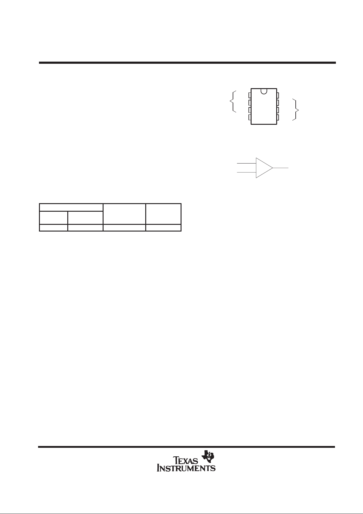
–
+
IN+
OUT
IN–
1
2
3
4
8
7
6
5
OUT
IN–
IN+
V
CC–
V
CC+
OUT
IN–
IN+
D OR P PACKAGE
(TOP VIEW)
AMP # 1
AMP # 2
symbol (each amplifier)
V
IO
Input offset voltage VO = 0
VO = 0
VO = 0
mV
nA
nA
I
IO
Input offset current
IIBI
nput bias current
V
I
Input voltage range
V/mV
RC4559
DUAL HIGH-PERFORMANCE OPERATIONAL AMPLIFIER
POST OFFICE BOX 655303 • DALLAS, TEXAS 75265
2
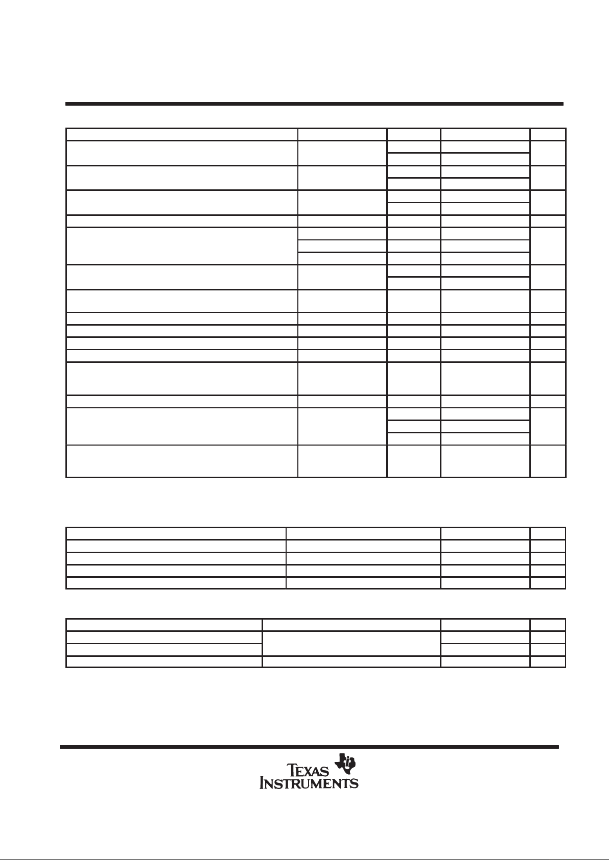
electrical characteristics at specified free-air temperature, V
CC+
= 15 V, V
CC–
= –15 V
PARAMETER TEST CONDITIONS
†
T
A
‡
MIN TYP MAX UNIT
25°C 2 6
Full Range 7.5
25°C 5 100
Full range 200
25°C 40 250
Full range 500
V
I
Input voltage range 25°C ±12 ±13 V
RL ≥ 3 kΩ 25°C ±12 ±13
V
OM
Maximum peak output voltlage swing RL = 600 Ω 25°C ±9.5 ±10 V
RL ≥ 2 kΩ Full range ±10
VO = ±10 V , 25°C 20 300
RL = 2 kΩ Full range 15
B
OM
Maximum output-swing bandwidth
V
OPP
= 20 V,
RL = 2 kΩ
25°C 24 32 kHz
B
1
Unity-gain bandwidth 25°C 3 4 MHz
r
i
Input resistance 25°C 0.3 1 MΩ
CMRR Common-mode rejection ratio VO = 0 25°C 80 100 dB
k
SVS
Supply voltage sensitivity (∆VIO/∆VCC) VO = 0 25°C 10 75 µV/V
V
n
Equivalent input noise voltage (closed loop)
AVD = 100,
RS = 1 kΩ,
f = 20 Hz to 20 kHz
25°C 1.4 2 µV
I
n
Equivalent input noise current f = 20 Hz to 20 kHz 25°C 25 pA
25°C 3.3 5.6
I
CC
Supply current (both amplifiers) No load, No signal 0°C 4 6.6 mA
70°C 3 5
Vo1/V
o2
Crosstalk attentuation
AVD = 100,
RS = 1 kΩ,
f = 10 kHz
25°C 90 dB
†
All characteristics are specified under open-loop operation, unless otherwise noted.
‡
Full range operating free-air temperature range is 0°C to 70°C.
matching characteristics at V
CC+
= 15 V, V
CC–
= –15 V, TA = 25°C
PARAMETER TEST CONDITIONS MIN TYP MAX
UNIT
V
IO
Input offset voltage VO = 0 ±0.2 mV
I
IO
Input offset current VO = 0 ±7.5 nA
I
IB
Input bias current VO = 0 ±15 nA
A
VD
Large-signal differential voltage amplification VO = ±10 V, RL = 2 kΩ ±1 dB
operating characteristics, V
CC+
= 15 V, V
CC–
= –15 V, TA = 25°C
PARAMETER TEST CONDITIONS MIN TYP MAX
UNIT
t
r
Rise time VI = 20 mV, RL = 2 kΩ, CL = 100 pF 80 µs
Overshoot 18%
SR Slew rate at unity gain VI = 10 mV, RL = 2 kΩ, CL = 100 pF 1.5 2 V/µs

IMPORTANT NOTICE
T exas Instruments and its subsidiaries (TI) reserve the right to make changes to their products or to discontinue
any product or service without notice, and advise customers to obtain the latest version of relevant information
to verify, before placing orders, that information being relied on is current and complete. All products are sold
subject to the terms and conditions of sale supplied at the time of order acknowledgement, including those
pertaining to warranty, patent infringement, and limitation of liability.
TI warrants performance of its semiconductor products to the specifications applicable at the time of sale in
accordance with TI’s standard warranty. Testing and other quality control techniques are utilized to the extent
TI deems necessary to support this warranty. Specific testing of all parameters of each device is not necessarily
performed, except those mandated by government requirements.
CERT AIN APPLICATIONS USING SEMICONDUCTOR PRODUCTS MAY INVOLVE POTENTIAL RISKS OF
DEATH, PERSONAL INJURY, OR SEVERE PROPERTY OR ENVIRONMENTAL DAMAGE (“CRITICAL
APPLICATIONS”). TI SEMICONDUCTOR PRODUCTS ARE NOT DESIGNED, AUTHORIZED, OR
WARRANTED TO BE SUITABLE FOR USE IN LIFE-SUPPORT DEVICES OR SYSTEMS OR OTHER
CRITICAL APPLICATIONS. INCLUSION OF TI PRODUCTS IN SUCH APPLICA TIONS IS UNDERST OOD TO
BE FULLY AT THE CUSTOMER’S RISK.
In order to minimize risks associated with the customer’s applications, adequate design and operating
safeguards must be provided by the customer to minimize inherent or procedural hazards.
TI assumes no liability for applications assistance or customer product design. TI does not warrant or represent
that any license, either express or implied, is granted under any patent right, copyright, mask work right, or other
intellectual property right of TI covering or relating to any combination, machine, or process in which such
semiconductor products or services might be or are used. TI’s publication of information regarding any third
party’s products or services does not constitute TI’s approval, warranty or endorsement thereof.
Copyright 1998, Texas Instruments Incorporated
 Loading...