

Page 1
查询RC4136DR供应商
RC4136, RM4136, RV4136
QUAD HIGH-PERFORMANCE OPERATIONAL AMPLIFIERS
SLOS072 – D2142, MARCH 1978–REVISED SEPTEMBER 1990
• Continuous-Short-Circuit Protection
• Wide Common-Mode and Differential
Voltage Ranges
• No Frequency Compensation Required
• Low Power Consumption
• No Latch-Up
• Unity Gain Bandwidth 3 MHz Typical
• Gain and Phase Match Between Amplifiers
• Designed to Be Interchangeable With
Raytheon RC4136, RM4136, and RV4136
• Low Noise...8 nV√Hz Typ at 1 kHz
description
The RC4136, RM4136, and RV4136 are quad
high-performance operational amplifiers with
each amplifier electrically similar to the uA741
except that offset null capability is not provided.
The high common-mode input voltage range and
the absence of latch-up make these amplifiers
ideal for voltage-follower applications. The
devices are short-circuit protected and the internal
frequency compensation ensures stability without
external components.
The RC4136 is characterized for operation from
0°C to 70°C, the RM4136 is characterized for
operation over the full military temperature range
of –55°C to 125°C, and the RV4136 is
characterized for operation from –40°C to 85°C.
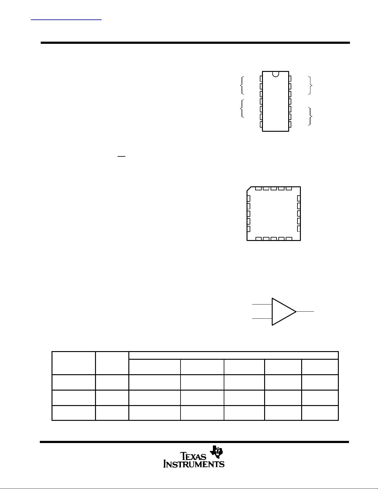
RM 4136 ...J OR W PACKAGE
ALL OTHERS ...D OR N PACKAGE
(T0P VIEW)
# 1
# 2
IN–
IN+
OUT
OUT
IN+
AMPL
AMPL
V
FK CHIP CARRIER PACKAGE
#1 OUT
NC
#2 OUT
NC
#2 IN+
1
2
3
4
5
IN–
6
7
CC–
RM4136
(T0P VIEW)
# 1 IN+
# 1 IN–
3 2 1 20 19
4
5
6
7
8
910111213
CC–
V
# 2 IN–
NC–No internal connection
symbol (each amplifier)
Noninverting
Input IN+
Inverting
Input IN–
NC
NC
+
–
IN–
14
IN+
13
OUT
12
V
11
OUT
10
IN+
9
IN–
8
# 4 IN–
# 4 IN+
18
17
16
15
14
# 3 IN–
# 3 IN+
CC+
#4 OUT
NC
V
NC
#3 OUT
AMPL
# 4
AMPL
# 3
CC+
Output
AVAILABLE OPTIONS
PACKAGE
T
A
0°C to
70°C
–40°C to
85°C
–55°C to
125°C
The D packages are available taped and reeled. Add the suffix R to the device type, (e.g., RC4136DR).
PRODUCTION DATA documents contain information current
as of publication date. Products conform to specifications per
the terms of Texas Instruments standard warranty . Production
processing does not necessarily include testing of all
parameters.
VIO MAX
at 25°C
6 mV RC4136D — — RC4136N —
4 mV
SMALL-OUTLINE CHIP CARRIER CERAMIC DIP PLASTIC DIP FLAT
(D) (FK) (J) (N) (W)
RV4136D RV4136N6 mV — —
POST OFFICE BOX 655303 • DALLAS, TEXAS 75265
—
RM4136W—RM4136JRM4136FK—
Copyright 1990, Texas Instruments Incorporated
On products compliant to MIL-STD-883, Class B, all
parameters are tested unless otherwise noted. On all
other products, production processing does not
necessarily include testing of all parameters.
1
Page 2
RC4136, RM4136, RV4136
QUAD HIGH-PERFORMANCE OPERATIONAL AMPLIFIERS
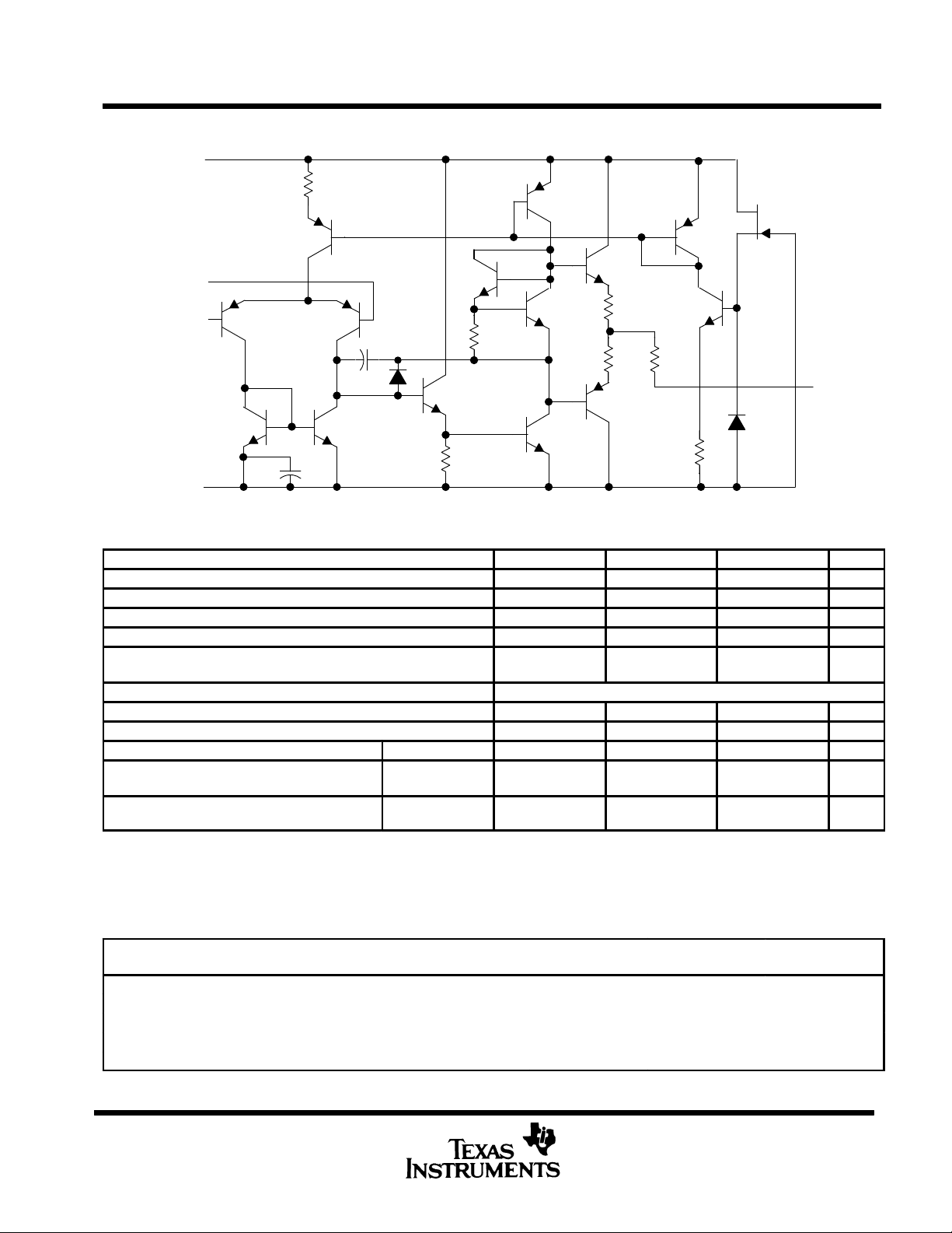
schematic (each amplifier)
V
CC+
Noninverting
Input IN+
Inverting
Input IN–
V
CC–
Output
absolute maximum ratings over operating free-air temperature range (unless otherwise noted)
RC4136 RM4136 RV4136 UNIT
Supply voltage V
Supply voltage V
Differential input voltage (see Note 2) ±30 ±30 ±30 V
Input voltage (any input, see Notes 1 and 3) ±15 ±15 ±15 V
Duration of output short-circuit to ground, one amplifier at a time
(see Note 4)
Continuous total dissipation See Dissipation Rating Table
Operating free-air temperature range 0 to 70 –55 to 125 –40 to 85 °C
Storage temperature range –65 to 150 –65 to 150 –65 to 150 °C
Case temperature for 60 seconds FK package — 260 — °C
Lead temperature 1,6 mm (1/16 inch)
from case for 60 seconds
Lead temperature 1,6 mm (1/16 inch)
from case for 10 seconds
NOTES: 1. All voltage values, unless otherwise noted, are with respect to the midpoint between V
2. Differential voltages are at the noninverting input terminal with respect to the inverting input terminal.
3. The magnitude of the input voltage must never exceed the magnitude of the supply voltage or 15 V, whichever is less.
4. Temperature and/or supply voltages must be limited to ensure that the dissipation rating is not exceeded.
PACKAGE
D 800 mW 7.6 mW/°C 45°C 608 mW 494 mW —
FK 800 mW 11.0 mW/°C77°C 800 mW 715 mW 275 mW
J 800 mW 11.0 mW/°C77°C 800 mW 715 mW 275 mW
N 800 mW 9.2 mW/°C63°C 736 mW 598 mW —
W 800 mW 8.0 mW/°C 50°C 640 mW 520 mW 200 mW
(see Note 1) 18 22 18 V
CC+
(see Note 1) –18 –22 –18 V
CC–
unlimited unlimited unlimited
J or W package — 300 — °C
D or N package 260 — 260 °C
TA ≤ 25°C
POWER RATING
DERATING
FACTOR
DISSIPATION RATING T ABLE
DERATE
ABOVE T
A
TA = 70°C
POWER RATING
and V
CC+
TA = 85°C
POWER RATING
CC–
.
TA = 125°C
POWER RATING
2
POST OFFICE BOX 655303 • DALLAS, TEXAS 75265
Page 3

recommended operating conditions
Supply voltage, V
Supply voltage, V
CC+
CC–
RC4136, RM4136, RV4136
QUAD HIGH-PERFORMANCE OPERATIONAL AMPLIFIERS
MIN NOM MAX UNIT
5 15 V
–5 –15 V
electrical characteristics at specified free-air temperature, V
RC4136 RM4136 RV4136
MIN TYP MAX MIN TYP MAX MIN TYP MAX
15 25 15
0.3*
5
888nV√Hz
6 13.7 6 13.3 6 13.7 mA
4.5 10 4.5 10 4.5 10
180 400 180 400 180 400 mW
135 300 135 300 135 300
V
IO
I
IO
I
IB
V
i
V
OM
A
VD
1
r
i
CMRR
k
SVS
V
n
I
CC
P
D
V01/V
PARAMETER TEST CONDITIONS
Input offset voltage
Input offset current
Input bias current
Input voltage range 25°C ±12 ±14 ±12 ±14 ±12 ±14 V
Maximum peak RL = 10 kΩ 25°C ±12 ±14 ±12 ±14 ±12 ±14
output voltage RL = 2 kΩ 25°C ±10 ±13 ±10 ±13 ±10 ±13 V
swing RL ≥ 2 kΩ Full range ±10 ±10 ±10
Large-signal
differential
voltage
amplification
Unity-gain
bandwith
Input resistance 25°C
Common-mode
rejection ratio
Supply voltage VCC = ±9 V to
sensitivity ±15 V, 25°C 30 150 30 150 30 150 µV/V
(∆VIO/∆VCC)V
Equivalent input
noise voltage
(closed-loop)
Supply current
(All four amplifiers)
Total power 25°C 150 340 150 340 150 340
dissipation MIN T
(All four amplifiers) MAX T
Crosstalk
02
attenuation
VO = 0
VO = 0
VO = 0
VO = ±10 V,
RL ≥ 2 kΩ
VO = 0,
RS = 50 Ω
= 0
O
AVD = 100,
BW = 1 Hz,
f = 1 kHz,
RS = 100 Ω
VO = 0,
No
load
VO = 0,
No
load
AVD = 100,
f = 10 kHz, 25°C 105 105 105 dB
RS = 1 kΩ
†
25°C 0.5 6 0.5 4 0.5 6
Full range 7.5 6 7.5
25°C 5 200 5 1.50 5 200
Full range 300 500 500
25°C 140 500 140 400 140 500
Full range 800 1500 1500
25°C 20 300 50 350 20 300
Full range
25°C 3 3.5 3 MHzB
25°C 7090 7090 7090
25°C
25°C 5 11.3 5 11.3 5 11.3
MIN T
A
MAX T
A
A
A
CC+
0.3*
= 15 V, V
5
CC–
0.3*
= –15 V
UNIT
mV
V/mV
5 MΩ
dB
* This parameter is not production tested.
†
All characteristics are measured under open-loop conditions with zero common-mode input voltage unless otherwise specified. Full range is 0°C
to 70°C for RC4136, –55°C to 125°C for RM4136, and –40°C to 85°C for RV4136.
nA
nA
POST OFFICE BOX 655303 • DALLAS, TEXAS 75265
3
Page 4

RC4136, RM4136, RV4136
QUAD HIGH-PERFORMANCE OPERATIONAL AMPLIFIERS
operating characteristics, V
PARAMETER TEST CONDITIONS UNIT
t
Rise time VI = 20 mV, RL = 2 kΩ, 0.13 0.13
r
Overshoot factor CL = 100 pF 5% 5%
= 15 V, V
CC+
VI = 10 V, RL = 2 kΩ,
CL = 100 pF
= –15 V, TA = 25°C
CC–
RC4136, RV4136 RM4136
MIN TYP MAX MIN TYP MAX
1.7 1.7
µs
V/µsSR Slew rate at unity gain
4
POST OFFICE BOX 655303 • DALLAS, TEXAS 75265
Page 5

IMPORTANT NOTICE
T exas Instruments (TI) reserves the right to make changes to its products or to discontinue any semiconductor
product or service without notice, and advises its customers to obtain the latest version of relevant information
to verify, before placing orders, that the information being relied on is current.
TI warrants performance of its semiconductor products and related software to the specifications applicable at
the time of sale in accordance with TI’s standard warranty. Testing and other quality control techniques are
utilized to the extent TI deems necessary to support this warranty. Specific testing of all parameters of each
device is not necessarily performed, except those mandated by government requirements.
Certain applications using semiconductor products may involve potential risks of death, personal injury, or
severe property or environmental damage (“Critical Applications”).
TI SEMICONDUCTOR PRODUCTS ARE NOT DESIGNED, INTENDED, AUTHORIZED, OR WARRANTED
TO BE SUITABLE FOR USE IN LIFE-SUPPORT APPLICATIONS, DEVICES OR SYSTEMS OR OTHER
CRITICAL APPLICATIONS.
Inclusion of TI products in such applications is understood to be fully at the risk of the customer. Use of TI
products in such applications requires the written approval of an appropriate TI officer . Questions concerning
potential risk applications should be directed to TI through a local SC sales office.
In order to minimize risks associated with the customer’s applications, adequate design and operating
safeguards should be provided by the customer to minimize inherent or procedural hazards.
TI assumes no liability for applications assistance, customer product design, software performance, or
infringement of patents or services described herein. Nor does TI warrant or represent that any license, either
express or implied, is granted under any patent right, copyright, mask work right, or other intellectual property
right of TI covering or relating to any combination, machine, or process in which such semiconductor products
or services might be or are used.
Copyright 1995, Texas Instruments Incorporated
 Loading...