

Page 1

User's Guide
SLAU239A–February 2008–Revised September 2015
TAS5342DDV6EVM
This user’s guide describes the operation of the evaluation module for the TAS5342 Digital Amplifier
Power Output Stage using the TAS5508B Digital Audio PWM Processor from Texas Instruments. The
user’s guide also provides measurement data and design information like schematic, bill of materials, and
PCB layout.
Contents
1 Overview...................................................................................................................... 3
1.1 TAS5342DDV6EVM Features..................................................................................... 4
1.2 PCB Key Map ....................................................................................................... 5
2 Quick Setup Guide........................................................................................................... 6
2.1 Electrostatic Discharge Warning.................................................................................. 6
2.2 Unpacking the EVM ................................................................................................ 7
2.3 Power Supply Setup................................................................................................ 7
2.4 Speaker Connection................................................................................................ 7
2.5 GUI Software Installation .......................................................................................... 8
3 Protection ..................................................................................................................... 8
3.1 Short-Circuit Protection and Fault-Reporting Circuitry......................................................... 8
3.2 Fault Reporting...................................................................................................... 8
4 TAS5342DDV6EVM Performance......................................................................................... 9
4.1 THD+N vs Power (BTL –4 Ω) ................................................................................... 11
4.2 THD+N vs Power (BTL –6 Ω) ................................................................................... 11
4.3 THD+N vs Power (BTL –8 Ω) ................................................................................... 12
4.4 THD+N vs Power (PBTL –2 Ω).................................................................................. 12
4.5 THD+N vs Power (PBTL –3 Ω).................................................................................. 13
4.6 THD+N vs Frequency (BTL –4 Ω) .............................................................................. 14
4.7 THD+N vs Frequency (BTL – 6 Ω).............................................................................. 14
4.8 THD+N vs Frequency (BTL –8 Ω) .............................................................................. 15
4.9 THD+N vs Frequency (PBTL –2 Ω)............................................................................. 15
4.10 THD+N vs Frequency (PBTL –3 Ω)............................................................................. 16
4.11 FFT Spectrum with –60-dBFS Tone (BTL) .................................................................... 16
4.12 FFT Spectrum With –60-dBFS Tone (PBTL).................................................................. 16
4.13 Idle Noise FFT Spectrum (BTL)................................................................................. 17
4.14 Idle Noise FFT Spectrum (PBTL) ............................................................................... 17
4.15 Channel Separation............................................................................................... 18
4.16 Frequency Response (BTL)...................................................................................... 19
4.17 Frequency Response (PBTL).................................................................................... 19
4.18 High-Current Protection (BTL)................................................................................... 19
4.19 High-Current Protection (PBTL)................................................................................. 20
4.20 Pop/Click (BTL).................................................................................................... 21
4.21 Pop/Click (PBTL).................................................................................................. 21
4.22 Output Stage Efficiency .......................................................................................... 22
4.23 Subwoofer Lineout THD vs Output Voltage ................................................................... 22
4.24 Subwoofer Lineout THD vs Frequency......................................................................... 23
4.25 Subwoofer Lineout Frequency Response...................................................................... 23
5 Related Documentation from Texas Instruments ...................................................................... 24
PurePath Digital, Equibit are trademarks of Texas Instruments.
Microsoft, Windows are registered trademarks of Microsoft Corporation.
SLAU239A–February 2008–Revised September 2015 TAS5342DDV6EVM
Submit Documentation Feedback
1
Copyright © 2008–2015, Texas Instruments Incorporated
Page 2

www.ti.com
5.1 Additional Documentation........................................................................................ 24
Appendix A Design Documents................................................................................................ 25
List of Figures
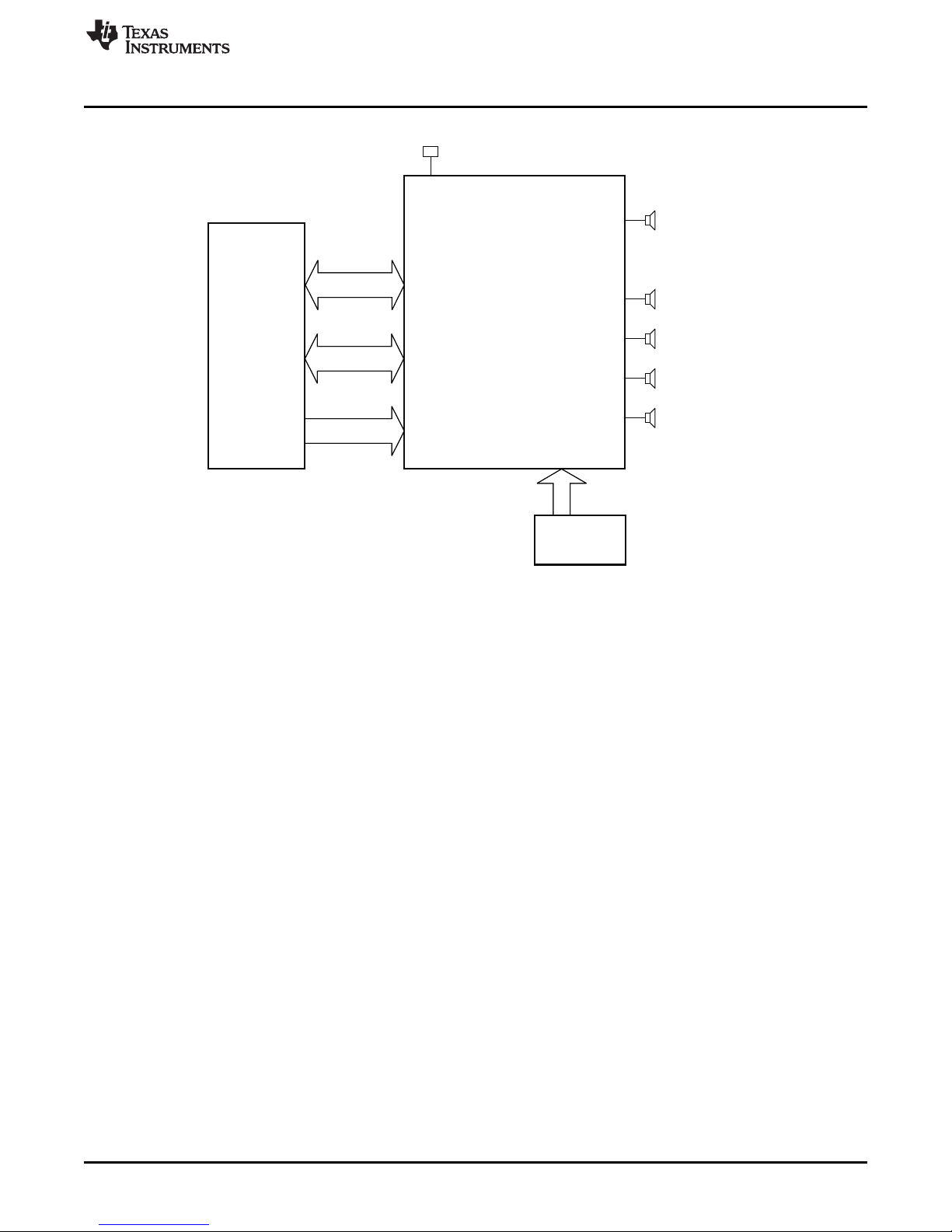
1 Integrated PurePath Digital™ Amplifier System......................................................................... 5
2 Physical Structure for the TAS5342DDV6EVM (Approximate Layout) ............................................... 6
3 TAS5508 GUI Window...................................................................................................... 8
4 THD+N vs Power (BTL – 4 Ω)............................................................................................ 11
5 THD+N vs Power (BTL –6 Ω) ............................................................................................ 12
6 THD+N vs Power (BTL –8 Ω) ............................................................................................ 12
7 THD+N vs Power (PBTL –2 Ω)........................................................................................... 13
8 THD+N vs Power (PBTL –3 Ω)........................................................................................... 13
9 THD+N vs Frequency (BTL –4 Ω) ....................................................................................... 14
10 THD+N vs Frequency (BTL – 6 Ω)....................................................................................... 14
11 THD+N vs Frequency (BTL –8 Ω) ....................................................................................... 15
12 THD+N vs Frequency (PBTL –2 Ω)...................................................................................... 15
13 THD+N vs Frequency (PBTL –3 Ω)...................................................................................... 16
14 FFT Spectrum with –60-dBFS Tone (BTL) ............................................................................. 16
15 FFT Spectrum with –60-dBFS Tone (PBTL)............................................................................ 17
16 Idle Noise FFT Spectrum (BTL).......................................................................................... 17
17 Idle Noise FFT Spectrum (PBTL) ........................................................................................ 18
18 Channel Separation........................................................................................................ 18
19 Frequency Response (BTL)............................................................................................... 19
20 Frequency Response (PBTL)............................................................................................. 19
21 High-Current Protection (BTL)............................................................................................ 20
22 High-Current Protection (PBTL).......................................................................................... 20
23 Pop/Click (BTL)............................................................................................................. 21
24 Pop/Click (PBTL)........................................................................................................... 21
25 Output Stage Efficiency ................................................................................................... 22
26 Subwoofer Lineout THD vs Output Voltage ............................................................................ 22
27 Subwoofer Lineout THD vs Frequency.................................................................................. 23
28 Subwoofer Lineout Frequency Response............................................................................... 23
1 TAS5342DDV6EVM Specification......................................................................................... 3
2 Recommended Supply Voltages for Power Stage ...................................................................... 7
3 Supply Adapter for System Power, Logic and Gate Driver Characteristics.......................................... 7
4 TAS5342 Warning/Error Signal Decoding................................................................................ 9
5 General Test Conditions.................................................................................................... 9
6 TAS5508B Register Settings............................................................................................... 9
7 Electrical Data................................................................................................................ 9
8 Audio Performance......................................................................................................... 10
9 Audio Performance Subwoofer Line Output ............................................................................ 10
10 Thermal Specification...................................................................................................... 10
11 Physical Specifications .................................................................................................... 11
12 Related Documentation from Texas Instruments ...................................................................... 24
2
TAS5342DDV6EVM SLAU239A–February 2008–Revised September 2015
List of Tables
Copyright © 2008–2015, Texas Instruments Incorporated
Submit Documentation Feedback
Page 3

www.ti.com
1 Overview
The TAS5342DDV6EVM PurePath Digital™ customer evaluation module demonstrates the integrated
circuits TAS5342DDV and TAS5508BPAG from Texas Instruments (TI).
The TAS5342DDV is a high-performance, integrated stereo Digital Amplifier Power Stage designed to
drive 4-Ω speakers at up to 100 W per channel. The device incorporates TI Equibit™ technology and is
designed to be used with TI Equibit™ modulators. This system requires only a simple passive
demodulation filter to deliver high-quality, high-efficiency audio amplification.
The TAS5508BPAG is a high-performance, 32-bit (24-bit input) multichannel PurePath Digital™ pulse
width modulator (PWM) based on Equibit™ technology with fully symmetrical AD modulation scheme. The
device also has digital audio processing (DAP) that provides 48-bit signal processing, advanced
performance, and a high level of system integration. The device has interfaces for headphone output and
power supply volume control (PSVC).
This EVM is configured with four BTL channels, one PBTL (parallel BTL) channel for the center channel,
and a subwoofer lineout using the DRV600 line driver.
The DRV600RTJ is a stereo line driver designed to allow the removal of the DC-blocking capacitors for
reduced component count and cost. The DRV600RTJ is ideal for single-supply electronics where size and
cost are critical design parameters. The DRV600RTJ is capable of driving two VRMS into a 600-Ω load
with a 3.3-V supply. The DRV600RTJ has a fixed gain of –1.5 V/V. Independent shutdown control for the
left and right audio channels is implemented.
This EVM, together with a TI input-USB board, is a complete 5-channel + subwoofer line-output digital
audio amplifier system which includes digital input (S/PDIF), analog inputs, interface to a personal
computer (PC), and DAP features like digital volume control, input and output mixers, automute, tone
controls, loudness, EQ filters, and dynamic range compression (DRC). Configuration options are available
for power stage failure protection.
Overview
Table 1. TAS5342DDV6EVM Specification
Key Parameters
Output stage supply voltage 0 V – 31.5 V
Number of channels 4 × BTL, 1 x PBTL
Load impedance BTL 4–8 Ω
Load impedance PBTL 2–8 Ω
Output power BTL 120 W / 4 Ω 10% THD or 87 W / 6 Ω / 10% THD
Output power PBTL 225 W / 2 Ω / 10% THD
DNR >102 dB
PWM processor TAS5508BPAG
Output stage TAS5342DDV
Other features Subwoofer line output
This 5-channel system plus subwoofer line output is designed for home theater applications such as A/V
receivers, DVD receivers, DVD mini-component systems, or home theater in a box (HTIB).
This document covers EVM specifications, audio performance and power efficiency measurements
graphs, and design documentation that includes schematics, parts list, layout, and mechanical design.
SLAU239A–February 2008–Revised September 2015 TAS5342DDV6EVM
Submit Documentation Feedback
3
Copyright © 2008–2015, Texas Instruments Incorporated
Page 4
Overview
www.ti.com
Gerber (layout) files are available at www.ti.com.
The EVM is delivered with cables and an Input-USB board to connect to an input source and be controlled
from a PC.
An external power adapter is required for supplying the voltage to the Input USB-2 Control Board. Refer to
the Power Supply Setup section for more information.
1.1 TAS5342DDV6EVM Features
• 5/6-channel PurePath Digital™ evaluation module
• Subwoofer line output (LFE Output).
• Self-contained protection system (short circuit and thermal).
• Standard I2S and I2C/control connector for TI input board
• Double-sided, plated-through PCB layout.
4
TAS5342DDV6EVM SLAU239A–February 2008–Revised September 2015
Copyright © 2008–2015, Texas Instruments Incorporated
Submit Documentation Feedback
Page 5
I2S
Bus
I2CBus
Example
TIInput- USB
board
8 Channel
Analog
Input
USB
Interface
Optical
and
Coaxia
l
S/P DIF
Input
ControlInterface
PowerSupply
5/6 Channel
SpeakerOutput
SubwooferLineOut
TAS5342DDV6EVM
MODULE
www.ti.com
Overview
1.2 PCB Key Map
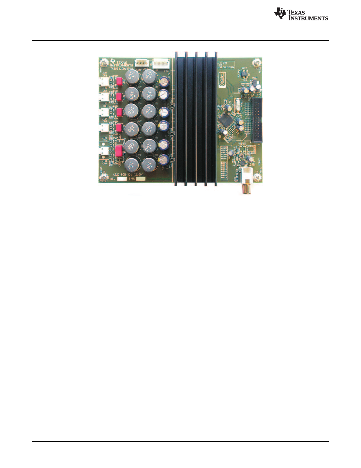
Physical structure for the TAS5342DDV6EVM is illustrated in Figure 2.
Figure 1. Integrated PurePath Digital™ Amplifier System
SLAU239A–February 2008–Revised September 2015 TAS5342DDV6EVM
Submit Documentation Feedback
Copyright © 2008–2015, Texas Instruments Incorporated
5
Page 6

SPEAKEROUTPUTS
TAS5508b
OUTPUT STAGE
CHANNEL 3
3.3V
Regulator
PSU
INTERFACE
(J901)
PSU
CONTROL
(J902)
INPUT SIGNAL & CONTROL
INTERFACE (J10)
SUBWOOFER
OUTPUT
(J600)
J101
BTL
J102
BTL
OUTPUT STAGE
CHANNEL 1
OUTPUT STAGE
CHANNEL 4
OUTPUT STAGE
CHANNEL 2
OUTPUT STAGE
CHANNEL 6
OUTPUT STAGE
CHANNEL 5
SPEAKEROUTPUTS
J103
BTL
J104
BTL
SPEAKEROUTPUTS
J117
PBTL
J107
BTL*
DRV600
J108
BTL*
*: ConfigOption
Quick Setup Guide
www.ti.com
Figure 2. Physical Structure for the TAS5342DDV6EVM (Approximate Layout)
2 Quick Setup Guide
This section describes the TAS5342DDV6EVM board in regards to power supplies and system interfaces.
Included is information regarding handling and unpacking, absolute operating conditions, and a description
of the factory default switch and jumper configuration. A step-by-step guide explains how to configure the
TAS5342DDV6EVM for device evaluation.
2.1 Electrostatic Discharge Warning
Many of the components on the TAS5342DDV6EVM are susceptible to damage by electrostatic discharge
(ESD). Customers are advised to observe proper ESD handling precautions when unpacking and handling
the EVM, including the use of a grounded wrist strap at an approved ESD workstation.
Failure to observe ESD handling procedures may result in damage to EVM
components.
CAUTION
6
TAS5342DDV6EVM SLAU239A–February 2008–Revised September 2015
Copyright © 2008–2015, Texas Instruments Incorporated
Submit Documentation Feedback
Page 7
www.ti.com
2.2 Unpacking the EVM
On opening the TAS5342DDV6EVM package, ensure that the following items are included:
• 1 pc. TAS5342DDV6EVM board using one TAS5508BPAG and three TAS5342DDV.
• 1 pc. TI Input USB Board 2 for interfacing TAS5342DDV6EVM with S/PDIF/analog sources and PC for
control.
• 1 pc. Signal and Control Interface IDC cable for connection to a TI Input USB Board 2.
• 1 pc. Cable for connecting Input-USB board to a USB port on a PC for TAS5508B control by software.
• 1 pc. Power supply cable for a regulated power supply (H-bridge supply).
If any of the items are missing, contact the Texas Instruments Product Information Center nearest you to
inquire about a replacement.
Connect Input-USB board to TAS5342DDV6EVM using the delivered IDC cable.
2.3 Power Supply Setup
To power up the EVM, two power supplies are needed. One for system power, logic, and gate-drive, and
one for output stage supply. The H-bridge power supply is connected to the EVM using the delivered
power cable White/Black, White/Black. The system, logic and gate drive power supply must be supplied
from an external 15-V, 1-A adapter. The characteristics of this adapter can be found in Table 3.
Description Voltage Limitations Current Requirement Cable
Output stage power supply 0 – 31.5 V 10 A White/Black
Quick Setup Guide
Table 2. Recommended Supply Voltages for Power Stage
Table 3. Supply Adapter for System Power, Logic and Gate Driver Characteristics
Description Requirement
DC Output Voltage 15 V
Output Current 1 A
Max Power Rating 15 W
DC Output Connector 5.5 mm x 2.1 mm x 10 mm center positive barrel plug
Applying voltages above the limitations given in Table 2 may cause permanent
damage to your hardware.
NOTE: The length of the power supply cable must be minimized. Increasing the length of the PSU
cable is equal to increasing the distortion for the amplifier at high output levels and low
frequencies.
2.4 Speaker Connection
Both positive and negative speaker outputs are floating and may not be
connected to ground (e.g., through an oscilloscope).
CAUTION
CAUTION
SLAU239A–February 2008–Revised September 2015 TAS5342DDV6EVM
Submit Documentation Feedback
7
Copyright © 2008–2015, Texas Instruments Incorporated
Page 8
Quick Setup Guide
2.5 GUI Software Installation
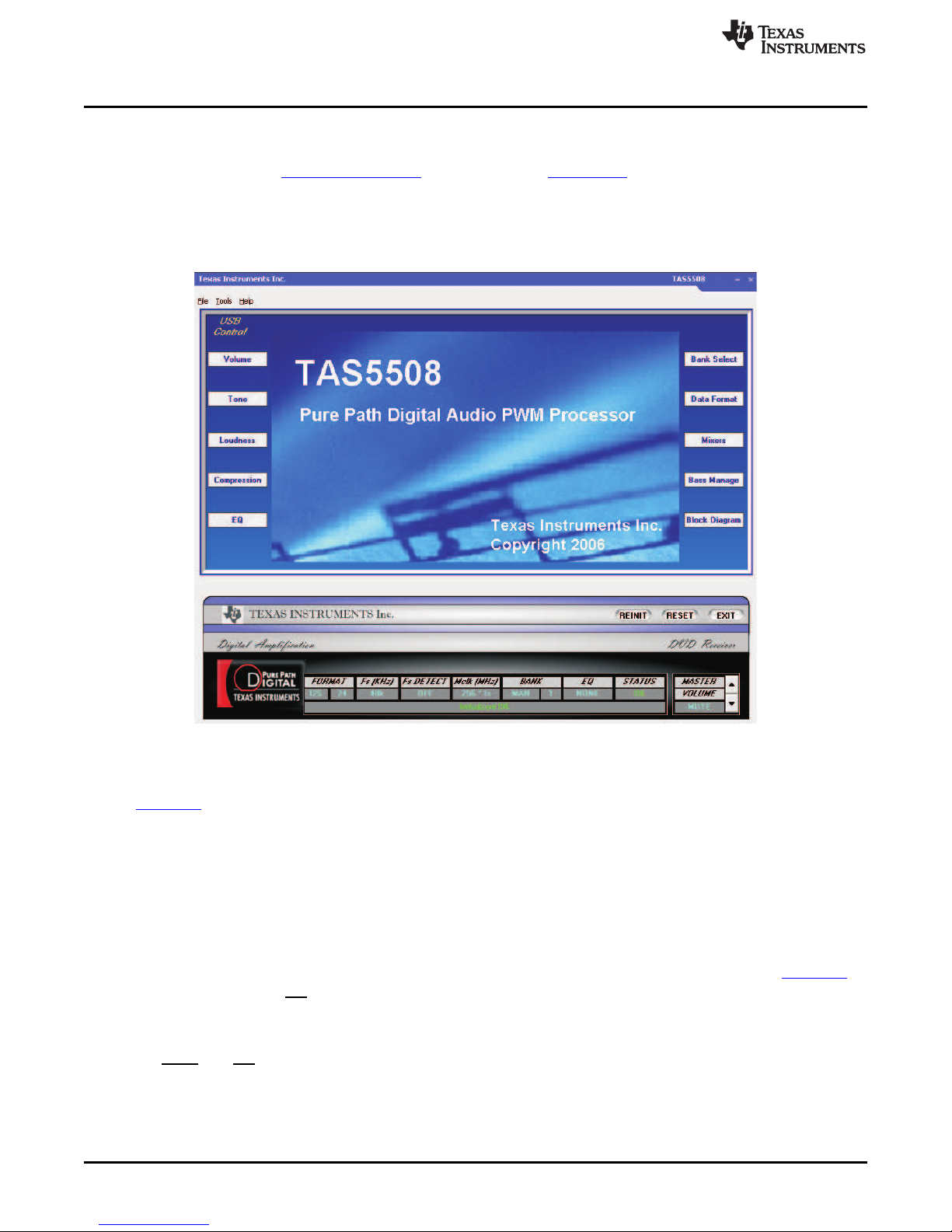
The TAS5508 GUI provides easy control of all registers in TAS5508B. The latest TAS5508 GUI can be
downloaded from the TAS5342DDV6EVM product folder on www.ti.com.
To install the software, run the setup file of the GUI.
After installation, turn on power supplies and connect USB cable to Input-USB board.
Start the GUI program from Microsoft®Windows®menu. Start up of the GUI takes a few seconds.
www.ti.com
For more advanced use of the GUI, see the GUI User’s Guide and data manual for TAS5508B
(SLES162).
3 Protection
This section describes the short-circuit protection and fault-reporting circuitry of the TAS5342 device.
3.1 Short-Circuit Protection and Fault-Reporting Circuitry
The TAS5342 is a self-protecting device that provides fault reporting (including high-temperature
protection and short-circuit protection). The TAS5342 is configured in back-end auto-recovery mode and
therefore resets automatically after all errors (M1, M2, and M3 is set low); see the data sheet (SLAS557)
for further explanation. This mean that the device restart itself after an error occasion and reports shortly
thereafter through the SD error signal.
3.2 Fault Reporting
The OTW and SD outputs from TAS5342 indicate fault conditions. See the TAS5342 data manual for a
description of these pins.
8
TAS5342DDV6EVM SLAU239A–February 2008–Revised September 2015
Figure 3. TAS5508 GUI Window
Copyright © 2008–2015, Texas Instruments Incorporated
Submit Documentation Feedback
Page 9
www.ti.com
Table 4. TAS5342 Warning/Error Signal Decoding
OTW SD Device Condition
0 0 High-temperature error and/or high-current error
0 1 High-temperature warning
1 0 Undervoltage lockout or high-current error
1 1 Normal operation, no errors/warnings
The temperature warning signals at the TAS5342DDV6EVM board are wired-OR to one temperature
warning signal (OTW – pin 22 in the control interface connector). Shutdown signals are wired-OR into one
shutdown signal (SD – pin 20 in the control interface connector).
The shutdown signals together with the temperature warning signal give chip-state information as
described in the Table 4. device fault-reporting outputs are open-drain outputs.
4 TAS5342DDV6EVM Performance
Table 5. General Test Conditions
General Test Conditions Notes
Output stage supply voltage: 31.5 V Laboratory power supply (EA-PS 7065-10A)
Load impedance BTL: 4–8 Ω
Load impedance PBTL: 2–4 Ω
Input signal 1 kHz sine
Sampling frequency 48 kHz
Gain setting in TAS5508B 0 dB
Measurement filter AES17 and AUX0025
TI input board Input-USB2 Rev 1
EVM configuration file Ver 1.00 TAS5342DDV6EVM Configuration (1.00).cfg
Note: These test conditions are used for all tests, unless otherwise specified.
TAS5342DDV6EVM Performance
Table 6. TAS5508B Register Settings
Register Register Value Notes
Modulation Index Limit 0x16 0x02 Set modulation index to 97.7%
Master Volume 0xD9 00 00 00 48 Master volume set to 0 dB
Note: These register settings are used for all test, unless otherwise specified.
Table 7. Electrical Data
Electrical Data Notes/Conditions
Output power, BTL, 4 Ω: 90 W 1 kHz, unclipped (0 dBFS), TA= 25°C
Output power, BTL, 4 Ω: 120 W 1 kHz, 10% THD+N, TA= 25°C
Output power, BTL, 6 Ω: 66 W 1 kHz, unclipped (0 dBFS), TA= 25°C
Output power, BTL, 6 Ω: 87 W 1 kHz, 10% THD+N, TA= 25°C
Output power, BTL, 8 Ω: 51 W 1 kHz, unclipped (0 dBFS), TA= 25°C
Output power, BTL, 8 Ω: 68 W 1 kHz, 10% THD+N, TA= 25°C
Output power, PBTL, 2 Ω: 170 W 1 kHz, unclipped (0 dBFS), TA= 25°C
Output power, PBTL, 2 Ω: 225 W 1 kHz, 10% THD+N, TA= 25°C
Output power, PBTL, 3 Ω: 130 W 1 kHz, unclipped (0 dBFS), TA= 25°C
Output power, PBTL, 3 Ω: 170 W 1 kHz, 10% THD+N, TA= 25°C
Maximum peak current, BTL: >10 A 1-kHz burst, 1 Ω, ROC= 27 kΩ
Maximum peak current, PBTL: >20 A 1-kHz burst, 1 Ω, ROC= 27 kΩ
Output stage efficiency: 90% 2 x channels, 8 Ω
Damping factor BTL: 8.5 1 kHz, relative to 4-Ω load
SLAU239A–February 2008–Revised September 2015 TAS5342DDV6EVM
Submit Documentation Feedback
9
Copyright © 2008–2015, Texas Instruments Incorporated
Page 10
TAS5342DDV6EVM Performance
Electrical Data Notes/Conditions
Damping factor PBTL: 9.4 1 kHz, relative to 2-Ω load
H-bridge supply current: <190 mA 1 kHz, -60-dBFS signal
Idle power consumption: 5.99 W H-bridge supply, –60-dBFS input signal
Audio Performance Notes/Conditions
THD+N, BTL, 4 Ω: 1 W <0.06 % 1 kHz
THD+N, BTL, 4 Ω: 10 W <0.15 % 1 kHz
THD+N, BTL, 4 Ω: 50 W <0.095 % 1 kHz
THD+N, BTL, 6 Ω: 1 W <0.08 % 1 kHz
THD+N, BTL, 6 Ω: 10 W <0.097 % 1 kHz
THD+N, BTL, 6 Ω: 50 W <0.08 % 1 kHz
THD+N, BTL, 8 Ω: 1 W <0.073 % 1 kHz
THD+N, BTL, 8 Ω: 10 W <0.085 % 1 kHz
THD+N, BTL, 8 Ω: 50 W <0.068 % 1 kHz
THD+N, PBTL, 2 Ω: 1 W <0.089 % 1 kHz
THD+N, PBTL, 2 Ω: 10 W <0.15 % 1 kHz
THD+N, PBTL, 2 Ω: 50 W <0.13 % 1 kHz
THD+N, PBTL, 2 Ω: 100 W <0.097 % 1 kHz
THD+N, PBTL, 2 Ω: 150 W <0.21 % 1 kHz
THD+N, PBTL, 3 Ω: 1 W <0.093 % 1 kHz
THD+N, PBTL, 3 Ω: 10 W <0.05 % 1 kHz
THD+N, PBTL, 3 Ω: 50 W <0.08 % 1 kHz
THD+N, PBTL, 3 Ω: 100 W <0.062 % 1 kHz
Dynamic Range: >102 dB Ref: rated power, A-weighted, AES17 filter, 4 ch avg
Noise Voltage: <160 μVrms A-weighted, AES17 filter
Click/Pop, DC step BTL: 14 mV Mute/unmute, no signal, 6 Ω
Click/Pop, DC step PBTL: 27 mV Mute/unmute, no signal, 4 Ω
Channel Separation: >61 dB 1 kHz,
Frequency Response: 0.0 / –0.8 dB 90 W / 4 Ω, unclipped (0 dBFS)
www.ti.com
Table 7. Electrical Data (continued)
Table 8. Audio Performance
Table 9. Audio Performance Subwoofer Line Output
Audio Performance Notes/Conditions
Full-scale output voltage swing, 0 dBFS: 2 VRMS 100 Hz, 10-kΩ load
Full-scale output voltage swing, 10% 2.32 VRMS 100 Hz, 10-kΩ load
THD+N:
THD+N, 10 kΩ: 1 V <0.017% 100 Hz
THD+N, 10 kΩ: 100 mV <0.013% 100 Hz
Frequency response: +1, –3 dB 20 Hz–1.7 kHz
Dynamic range: >105.5 dB 20 Hz–1.7 kHz
Noise voltage: <11 μV 20 Hz–1.7 kHz
Thermal Specification** T
Idle, all channels switching 32°C 1 kHz, 15 min, –60 dBFS signal, TA= 25°C
4x12.5 W, 4 Ω + 1x25 W , 2 Ω (1/8 power) 58°C 1 kHz, 1 hour, TA= 25°C
2x100 W, 4 Ω 78°C 1 kHz, 5 min, TA= 25°C
*Measured on surface of heatsink
10
TAS5342DDV6EVM SLAU239A–February 2008–Revised September 2015
Table 10. Thermal Specification
* Notes/Conditions
HEATSINK
Copyright © 2008–2015, Texas Instruments Incorporated
Submit Documentation Feedback
Page 11
0.005
10
0.01
0.02
0.05
0.1
0.2
0.5
1
2
5
20m 20050m 100m 200m 500m
1 2 5
10 20 50 100
Power-W
THD+N-TotalHarmonicDistortion+Noise-%
www.ti.com
Physical Specifications Notes/Conditions
PCB dimensions: 124 × 150 × 54 Width × Length × Height (mm)
Total weight: 370 gr Components + PCB + Heatsink + Mechanics
Note: All electrical and audio specifications are typical values.
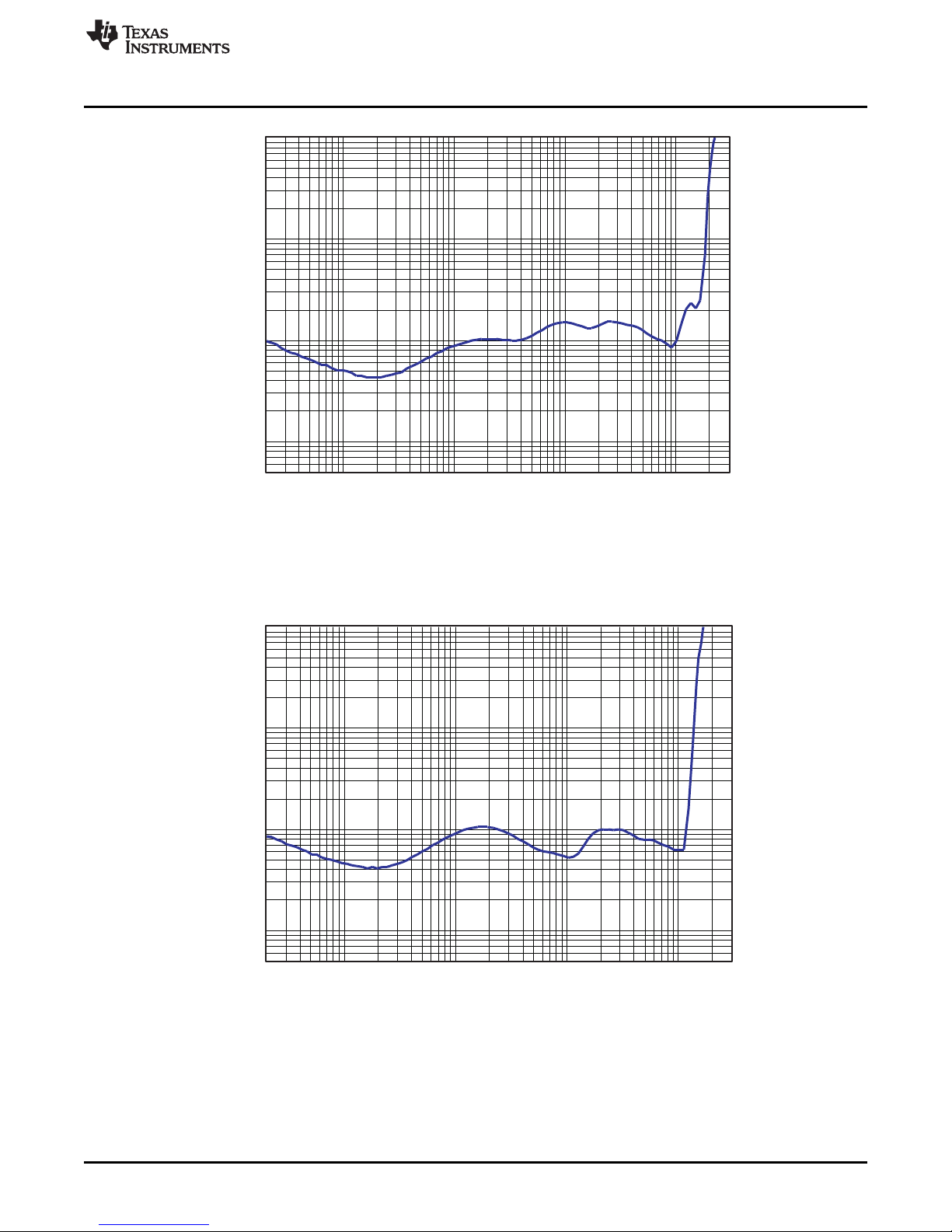
4.1 THD+N vs Power (BTL –4 Ω)
Gain: +2.5 dB set in TAS5508B
TAS5342DDV6EVM Performance
Table 11. Physical Specifications
Figure 4. THD+N vs Power (BTL – 4 Ω)
4.2 THD+N vs Power (BTL –6 Ω)
Gain: +2.5 dB set in TAS5508B
SLAU239A–February 2008–Revised September 2015 TAS5342DDV6EVM
Submit Documentation Feedback
Copyright © 2008–2015, Texas Instruments Incorporated
11
Page 12
0.005
10
0.01
0.02
0.05
0.1
0.2
0.5
1
2
5
THD+N-TotalHarmonicDistortion+Noise-%
20m 50m 100m 200m 500m 1 2 5 10 20 50 100
Power-W
0.005
10
0.01
0.02
0.05
0.1
0.2
0.5
1
2
5
THD+N-TotalHarmonicDistortion+Noise-%
20m 20050m 100m 200m 500m 1 2 5 10 20 50 100
Power-W
TAS5342DDV6EVM Performance
www.ti.com
Figure 5. THD+N vs Power (BTL –6 Ω)
4.3 THD+N vs Power (BTL –8 Ω)
Gain: +2.5 dB set in TAS5508B
Figure 6. THD+N vs Power (BTL –8 Ω)
4.4 THD+N vs Power (PBTL –2 Ω)
Gain: +2.5 dB set in TAS5508B
12
TAS5342DDV6EVM SLAU239A–February 2008–Revised September 2015
Copyright © 2008–2015, Texas Instruments Incorporated
Submit Documentation Feedback
Page 13
20m 30050m 100m200m 500m 1 2 5 10 20 50 100
Power-W
0.005
10
0.01
0.02
0.05
0.1
0.2
0.5
1
2
5
THD+N-TotalHarmonicDistortion+Noise-%
20m 30050m 100m 200m 500m 1 2 5 10 20 50 100
Power-W
0.005
10
0.01
0.02
0.05
0.1
0.2
0.5
1
2
5
THD+N-TotalHarmonicDistortion+Noise-%
www.ti.com
TAS5342DDV6EVM Performance
Figure 7. THD+N vs Power (PBTL –2 Ω)
4.5 THD+N vs Power (PBTL –3 Ω)
Gain: +2.5 dB set in TAS5508B
Figure 8. THD+N vs Power (PBTL –3 Ω)
SLAU239A–February 2008–Revised September 2015 TAS5342DDV6EVM
Submit Documentation Feedback
Copyright © 2008–2015, Texas Instruments Incorporated
13
Page 14
0.001
5
0.002
0.005
0.01
0.02
0.05
0.1
0.2
0.5
1
2
20 20k50 100 200 500 1k 2k 5k 10k
f-Frequency-Hz
1W
10W
62W
THD+N-TotalHarmonicDistortion+Noise-%
0.001
5
0.002
0.005
0.01
0.02
0.05
0.1
0.2
0.5
1
2
20 20k50 100 200 500 1k 2k 5k 10k
f-Frequency-Hz
1W
10W
86W
THD+N-TotalHarmonicDistortion+Noise-%
TAS5342DDV6EVM Performance
4.6 THD+N vs Frequency (BTL –4 Ω)
Figure 9. THD+N vs Frequency (BTL –4 Ω)
www.ti.com
4.7 THD+N vs Frequency (BTL – 6 Ω)
Figure 10. THD+N vs Frequency (BTL – 6 Ω)
14
TAS5342DDV6EVM SLAU239A–February 2008–Revised September 2015
Copyright © 2008–2015, Texas Instruments Incorporated
Submit Documentation Feedback
Page 15
0.001
5
0.002
0.005
0.01
0.02
0.05
0.1
0.2
0.5
1
2
THDN-TotalHarmonicDistortion+Noise-%
20 20k50 100 200 500 1k 2k 5k 10k
f-Frequency-Hz
1W
10W
172W
20 20k50 100 200 500 1k 2k 5k 10k
f-Frequency-Hz
0.001
5
0.002
0.005
0.01
0.02
0.05
0.1
0.2
0.5
1
2
THDN-TotalHarmonicDistortion+Noise-%
1W
10W
48W
www.ti.com
4.8 THD+N vs Frequency (BTL –8 Ω)
Figure 11. THD+N vs Frequency (BTL –8 Ω)
TAS5342DDV6EVM Performance
4.9 THD+N vs Frequency (PBTL –2 Ω)
Figure 12. THD+N vs Frequency (PBTL –2 Ω)
SLAU239A–February 2008–Revised September 2015 TAS5342DDV6EVM
Submit Documentation Feedback
Copyright © 2008–2015, Texas Instruments Incorporated
15
Page 16

0 22k2k 4k 6k 8k 10k 12k 14k 16k 18k 20k
f-Frequency-Hz
-150
0
-140
-130
-120
-110
-100
-90
-80
-70
-60
-50
-40
-30
-20
-10
FFT-Spectrum-dB
0.001
5
0.002
0.005
0.01
0.02
0.05
0.1
0.2
0.5
1
2
THDN-TotalHarmonicDistortion+Noise-%
20 20k50 100 200 500 1k 2k 5k 10k
f-Frequency-Hz
1W
10W
125W
TAS5342DDV6EVM Performance
4.10 THD+N vs Frequency (PBTL –3 Ω)
Figure 13. THD+N vs Frequency (PBTL –3 Ω)
www.ti.com
4.11 FFT Spectrum with –60-dBFS Tone (BTL)
Reference voltage is 19.09 V. FFT size 16k.
4.12 FFT Spectrum With –60-dBFS Tone (PBTL)
Reference voltage is 18.7 V. FFT size 16k.
16
TAS5342DDV6EVM SLAU239A–February 2008–Revised September 2015
Figure 14. FFT Spectrum with –60-dBFS Tone (BTL)
Copyright © 2008–2015, Texas Instruments Incorporated
Submit Documentation Feedback
Page 17

0 85k5k 10k 15k 20k 25k 30k 35k 40k 45k 50k 55k 60k 65k 70k 75k 80k
f-Frequency-Hz
0
-140
-130
-120
-110
-100
-90
-80
-70
-60
-50
-40
-30
-20
-10
IdleNoiseSpectrum-dB
0 22k2k 4k 6k 8k 10k 12k 14k 16k 18k 20k
f-Frequency-Hz
-150
0
-140
-130
-120
-110
-100
-90
-80
-70
-60
-50
-40
-30
-20
-10
FFT-Spectrum-dB
www.ti.com
TAS5342DDV6EVM Performance
Figure 15. FFT Spectrum with –60-dBFS Tone (PBTL)
4.13 Idle Noise FFT Spectrum (BTL)
Automute disabled – Register x04h set to x60h. Reference voltage is 19.02 V. FFT size 16k.
4.14 Idle Noise FFT Spectrum (PBTL)
Automute disabled – Register x04h set to x60h. Reference voltage is 18.75 V. FFT size 16k.
SLAU239A–February 2008–Revised September 2015 TAS5342DDV6EVM
Submit Documentation Feedback
Figure 16. Idle Noise FFT Spectrum (BTL)
Copyright © 2008–2015, Texas Instruments Incorporated
17
Page 18

-80
10
-70
-60
-50
-40
-30
-20
-10
0
20 20k50 100 200 500 1k 2k 5k 10k
f-Frequency-Hz
InputSignal-dB
Channel1
Channel2
0
-140
-130
-120
-110
-100
-90
-80
-70
-60
-50
-40
-30
-20
-10
IdleNoiseSpectrum-dB
0 5k 10k 15k 20k
f-Frequency-Hz
25k 30k 35k 40k 45k 50k 55k 60k 65k 70k 75k 80k 85k
TAS5342DDV6EVM Performance
www.ti.com
Figure 17. Idle Noise FFT Spectrum (PBTL)
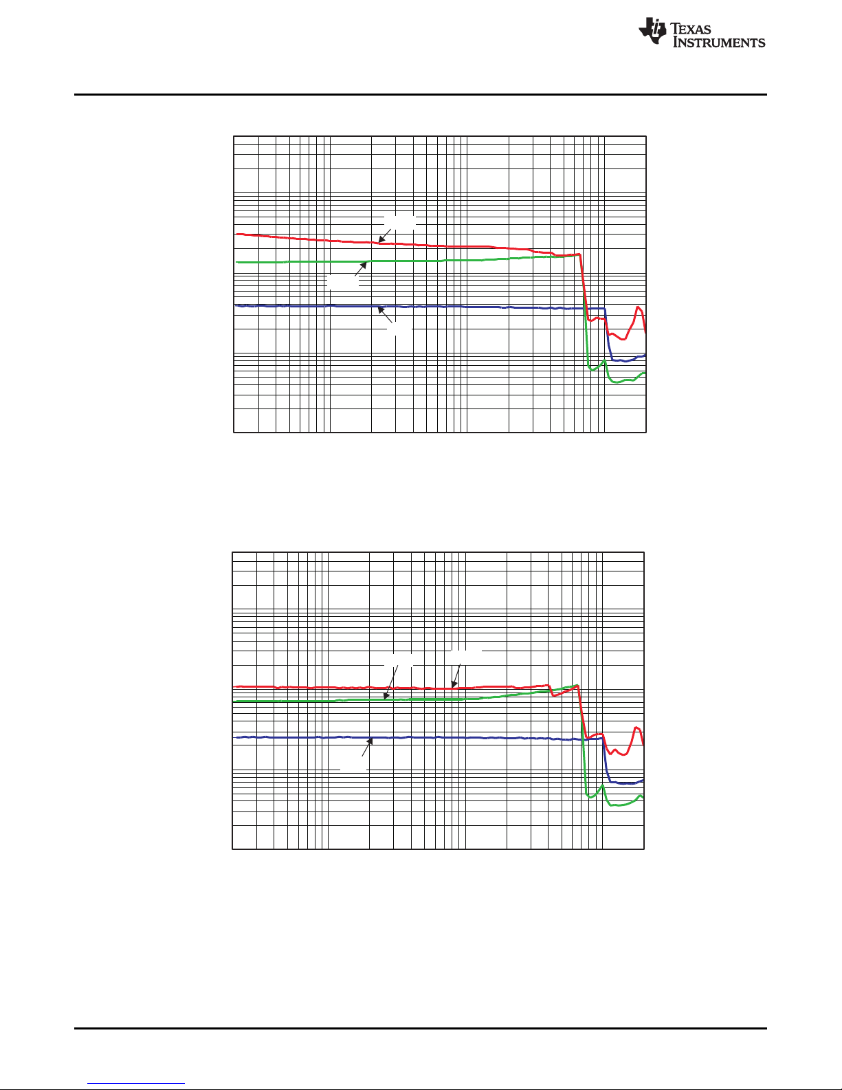
4.15 Channel Separation
Channel separation is tested for two channels in different package, channel 1 and channel 2. 4-Ω loads
are used for both channels. Channel 1 input signal is 0 dBFS, channel 2 muted. Reference voltage 19
Vrms
18
TAS5342DDV6EVM SLAU239A–February 2008–Revised September 2015
Figure 18. Channel Separation
Copyright © 2008–2015, Texas Instruments Incorporated
Submit Documentation Feedback
Page 19

-10
10
-8
-6
-4
-2
0
2
4
6
8
20 20k50 100 200 500 1k 2k 5k 10k
f-Frequency-Hz
InputSignal-dB
8W
4W
3W
2W
-10
10
-8
-6
-4
-2
0
2
4
6
8
20 20k50 100 200 500 1k 2k 5k 10k
f-Frequency-Hz
InputSignal-dB
8W
6W
4W
www.ti.com
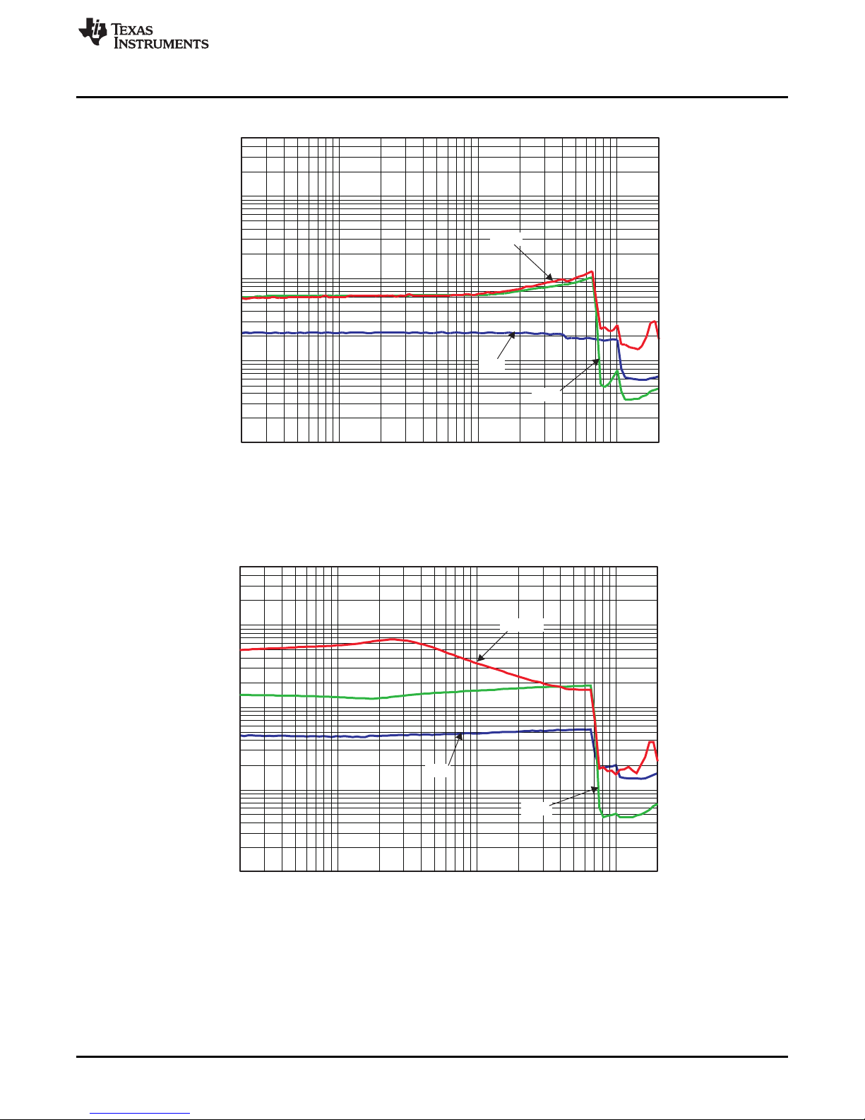
4.16 Frequency Response (BTL)
Measurement bandwidth filter 80 kHz.
TAS5342DDV6EVM Performance
Figure 19. Frequency Response (BTL)
4.17 Frequency Response (PBTL)
Measurement bandwidth filter 80 kHz.
4.18 High-Current Protection (BTL)
Input 1-kHz bursted signal, load 1 Ω
SLAU239A–February 2008–Revised September 2015 TAS5342DDV6EVM
Submit Documentation Feedback
Figure 20. Frequency Response (PBTL)
Copyright © 2008–2015, Texas Instruments Incorporated
19
Page 20

dx=505.9 sm
dy=47.31V
-30
30
-27.5
-22.5
-20
-17.5
-15
-12.5
-10
-7.5
-5
-2.5
0
2.5
5
7.5
10
12.5
15
17.5
20
25
27.5
23.19
-24.12
0
3m
250m
500m 750m
1m
1.25m
1.5m
1.75m
2m
2.25m
2.5m
2.75m
1.376m
1.882m
t-TIME-sec
PeakCurrent- A
-20
20
-17.5
-15
-10
-7.5
-5
-2.5
0
2.5
5
7.5
12.5
15
17.5
10.97
-11.12
0 3m
500m
2m
2.5m
1m
.9176m
t-TIME-sec
1.412m
dx=494.1 sm
dy=22.09V
PeakCurrent- A
TAS5342DDV6EVM Performance
www.ti.com
Figure 21. High-Current Protection (BTL)
4.19 High-Current Protection (PBTL)
Input 1-kHz bursted signal, load 1 Ω.
20
Figure 22. High-Current Protection (PBTL)
TAS5342DDV6EVM SLAU239A–February 2008–Revised September 2015
Copyright © 2008–2015, Texas Instruments Incorporated
Submit Documentation Feedback
Page 21

-40m
40m
-35m
-30m
-25m
-20m
-15m
-10m
-5m
0
5m
10m
15m
20m
25m
30m
35m
0
4m
500m
1m 1.5m 2m 2.5m
3m
3.5m
t-Time-sec
Voltage-V
-40m
40m
-35m
-30m
-25m
-20m
-15m
-10m
-5m
0
5m
10m
15m
20m
25m
30m
35m
0 4m
500m
1m 1.5m 2m 2.5m 3m 3.5m
t-Time-sec
Voltage-V
www.ti.com
4.20 Pop/Click (BTL)
No input signal applied. The measurement results are presented in time domain.
Test with automute disabled – Register x04h set to x60h. No input signal applied. Load 4 Ω.
TAS5342DDV6EVM Performance
4.21 Pop/Click (PBTL)
No input signal applied. The measurement results are presented in time domain.
Test with automute disabled – Register x04h set to x60h. No input signal applied. Load 2 Ω.
SLAU239A–February 2008–Revised September 2015 TAS5342DDV6EVM
Submit Documentation Feedback
Figure 23. Pop/Click (BTL)
Figure 24. Pop/Click (PBTL)
Copyright © 2008–2015, Texas Instruments Incorporated
21
Page 22

0.001
10
0.002
0.005
0.01
0.02
0.05
0.1
0.2
0.5
1
2
5
20m 350m 100m 200m 500m 1 2
V -OutputVoltage-V
O
THD-TotalHarmonicDistortion-%
0
100
5
10
15
20
25
30
35
40
45
55
60
65
70
75
80
85
95
91.06
51.85
0 20020 40 60 80 100 120 140 160 180
186
7.71
2CHOutputPower-W
Efficiency-%
dx=178.3FFS
dy=39.22V
TAS5342DDV6EVM Performance
4.22 Output Stage Efficiency
Efficiency is tested with two channels carrying an 8-Ω load. The board has been preheated for 1 hour at
1/8 output power.
www.ti.com
Figure 25. Output Stage Efficiency
4.23 Subwoofer Lineout THD vs Output Voltage
Gain: +2.5 dB set in TAS5508B. 100-Hz input
22
Figure 26. Subwoofer Lineout THD vs Output Voltage
TAS5342DDV6EVM SLAU239A–February 2008–Revised September 2015
Copyright © 2008–2015, Texas Instruments Incorporated
Submit Documentation Feedback
Page 23

-40
10
-35
-30
-25
-20
-15
-10
-5
0
5
10 20k20 50 100 200 500 1k 2k 5k 10k
f-Frequency-Hz
LineOut-dB
0.001
5
0.002
0.005
0.01
0.02
0.05
0.1
0.2
0.5
1
2
10 1k20 50 100 200 500
f-Frequency-Hz
THDN-TotalHarmonicDistortion+Noise-%
0.01VRMS
0.1VRMS
1.96VRMS(-0.2dBFS)
www.ti.com
4.24 Subwoofer Lineout THD vs Frequency
Load 10 kΩ
TAS5342DDV6EVM Performance
Figure 27. Subwoofer Lineout THD vs Frequency
4.25 Subwoofer Lineout Frequency Response
Measurement bandwidth filter 80 kHz. Load 10 kΩ.
SLAU239A–February 2008–Revised September 2015 TAS5342DDV6EVM
Submit Documentation Feedback
Figure 28. Subwoofer Lineout Frequency Response
Copyright © 2008–2015, Texas Instruments Incorporated
23
Page 24

Related Documentation from Texas Instruments
5 Related Documentation from Texas Instruments
Table 12 contains a list of data manuals that have detailed descriptions of the integrated circuits used in
the design of the TAS5342DDV6EVM. The data manuals can be obtained at the URL http://www.ti.com.
Table 12. Related Documentation from
Texas Instruments
Part Number Literature Number
TAS5508B SLES162
TAS5342 SLAS557
DRV600 SLOS536
TLV271 SLOS351
TPS3825-33 SLVS165
TLV1117-33C SLVS561
5.1 Additional Documentation
1. PC Configuration Tool for TAS5508 (TAS5508 GUI ver. 4.0 or later)
2. System Design Considerations for True Digital Audio Power Amplifiers application report (SLAA117)
3. Digital Audio Measurements application report (SLAA114)
4. PSRR for PurePath Digital™ Audio Amplifiers application report (SLEA049)
5. Power Rating in Audio Amplifiers application report (SLEA047)
6. PurePath Digital™ AM Interference Avoidance application report (SLEA040)
7. Click and Pop Measurements Technique application report (SLEA044)
8. Power Supply Recommendations for DVD-Receivers application report (SLEA027)
9. Implementation of Power Supply Volume Control application report (SLEA038)
www.ti.com
24
TAS5342DDV6EVM SLAU239A–February 2008–Revised September 2015
Copyright © 2008–2015, Texas Instruments Incorporated
Submit Documentation Feedback
Page 25

Appendix A
SLAU239A–February 2008–Revised September 2015
Design Documents
This appendix comprises design documents pertaining to the TAS5162DDV6EVM evaluation module. The
documents are presented in the following order.
• Schematic (8 pages)
• Parts List (2 pages)
• PCB Specification (1 page)
• PCB Layers (4 pages)
• Heat-Sink Drawing (1 page)
SLAU239A–February 2008–Revised September 2015 Design Documents
Submit Documentation Feedback
25
Copyright © 2008–2015, Texas Instruments Incorporated
Page 26

5
5
4
4
3
3
2
2
1
1
D D
C C
B B
A A
Rev:
Page Title:
TI
Home Audio Amplifiers
ALL RIGHTS RESERVED
TEXAS INSTRUMENTS INCORPORATED
Project:
File Name:
Date:
Engineer:
Page: of
Size:
AUDIO/IMAGING GROUP
A2
2.00
Jonas L. Holm
TAS5342DDV6EVM - 5.1 Digital Amplifier Design
A820-SCH-001.DSN
TAS5342DDV6EVM
Friday, November 09, 2007 1 8
/ Parts List 2.00
TAS5342DDV6EVM
Page
1/8: Front Page and Schematic Disclaimer
2/8: Overview - Modulator, Input/Output and Line Output Connectors
3/8: 2 Channel BTL Power Stage
4/8: 2 Channel BTL Power Stage
7/8: Power Supplies & EEPROM
Design Name:
Version:
Date:
Design Engineer:
Audio Configuration:
Interfaces:
File Name: A820-SCH-001.DSN
2.00
5.Nov 2007
Jonas Holm (jlh@ti.com)
5.1 PurePath Digital Amplifier Design
1 x TAS5508b, 3 x TAS5342DDV
Setup:
Type: Mass Market Evaluation Module
4 Ohm (BTL) and 2 Ohm (PBTL) Speaker Loads
TI
Copyright 2007 Texas Instruments, Inc - All rights reserved - The TI and PurePath Digital logos are trademarks of Texas Instruments.
+31.5 V H-Bridge Supply Voltage
Performance: 80 W / 4 Ohm (BTL) unclipped, or 100 W / 4 Ohm (BTL) 10% THD+N
102 dB Dynamic Range
8/8: Mechanics
5/8: 1 Channel PBTL Power Stage
J10: 26 pin IDC Header for Control, I2C, +5V, +12V and for I2S Audio
J101-J104, J107, J108, J117: 2 pin 3.96mm Headers for Speakers
J901: 4 pin 3.96mm Header for H-Bridge Supply
6/8: Subwoofer Line Out
J600: RCA Jack for Subwoofer Line Out
J902: 5 pin 2.54 mm Header for PSVC Interface
SCHEMATIC DISCLAIMER
The preliminary schematic information and materials ("Materials") provided here are provided by Texas Instruments
Incorporated ("TI") as a service to its customers and/or suppliers, and may be used for informational purposes only, and
only subject to the following terms. By downloading or viewing these Materials, you are signifying your assent to these
terms.
1.) These preliminary evaluation schematics are intended for use for PRELIMINARY ENGINEERING
DEVELOPMENT AND EVALUATION PURPOSES ONLY and are not considered by Texas Instruments to be fit as a
basis for establishing production products or systems. This information may be incomplete in several respects, including
but not limited to information relating to required design, marketing, and/or manufacturing-related protective
considerations and product safety measures typically found in the end-product incorporating the
goods.
2.) Accordingly, neither TI nor its suppliers warrant the accuracy or completeness of the information, text,
graphics, links or other items contained within the Materials. TI may make changes to the Materials, or to the products
described therein, at any time without notice. TI makes no commitment to update the Materials.
3.) TI assumes no liability for applications assistance, customer product design, software performance, or services
that may be described or referenced in the Materials. The user assumes all responsibility and liability for proper and safe
design and handling of goods. Accordingly, the user indemnifies TI from all claims arising from its use of the Materials.
4.) TI currently deals with various customers for products, and therefore our arrangement with the user will not be
exclusive. TI makes no representations regarding the commercial availability of non-TI components that may be
referenced in the Materials.
5.) No license is granted under any patent right or other intellectual property right of TI covering or relating to any
combination, machine, or process in which such TI products or services might be or are used. Except as expressly
provided herein, TI and its suppliers do not grant any express or implied right to you under any patents, copyrights,
trademarks, or trade secret information.
6.) Performance tests and ratings, to the extent referenced in the Materials, are measured using specific computer
systems and/or components and reflect the approximate performance of TI products as measured by those tests. Any
difference in system hardware or software design or configuration may affect actual performance. Buyers should consult
other sources of information to evaluate the performance of systems or components they are considering purchasing.
7.) Resale of TI's products or services with statements different from or beyond the parameters stated by TI for that
product or service in official TI data books or data sheets voids all express and any implied warranties for the associated
TI product or service, and is an unfair and deceptive business practice, and TI is not responsible for any such use.
8.) The Materials are copyrighted and any unauthorized use may violate copyright, trademark, and other laws. You
may only download one copy for your internal use only, unless you are specifically licensed to do otherwise by TI in
writing. This is a license, not a transfer of title, and is subject to the following restrictions: You may not: (a) modify the
Materials (including any associated warranties, conditions, limitations or notices) or use them for any commercial
purpose, or any public display, performance, sale or rental; (b) decompile, reverse engineer, or disassemble software
Materials except and only to the extent permitted by applicable law; (c) remove any copyright or other proprietary notices
from the Materials; (d) transfer the Materials to another person. You agree to prevent any unauthorized copying of the
Materials. TI may terminate this license at any time if you are in breach of the terms of this Agreement. Upon termination,
you will immediately destroy the Materials.
9.) THE MATERIALS ARE PROVIDED "AS IS" WITHOUT ANY EXPRESS OR IMPLIED
WARRANTY OF ANY KIND INCLUDING WARRANTIES OF MERCHANTABILITY,
NONINFRINGEMENT OF INTELLECTUAL PROPERTY, OR FITNESS FOR ANY PARTICULAR
PURPOSE. IN NO EVENT SHALL TI OR ITS SUPPLIERS BE LIABLE FOR ANY DAMAGES
WHATSOEVER (INCLUDING, WITHOUT LIMITATION, DAMAGES FOR LOSS OF PROFITS, BUSINESS
INTERRUPTION, LOSS OF INFORMATION) ARISING OUT OF THE USE OF OR INABILITY TO USE
THE MATERIALS, EVEN IF TI HAS BEEN ADVISED OF THE POSSIBILITY OF SUCH DAMAGES.
NOTE1
Schematic Disclaimer Preliminary
Page 27

5
5
4
4
3
3
2
2
1
1
D D
C C
B B
A A
VALID
/SD
/TW
/SD
/TW
VALID
/RESET
/RESET_MODULATOR
SDIN3
SDIN2
SDIN1
SCL-A
SDA-A
LRCLK
SCLK
PSVC
SDIN4
VALID
/RESET_MODULATOR
MCLK
/HP_SEL
/PDN
/MUTE
/BKND_ERR
/SD
/TW
VALID
/RESET
SDA-A
SCL-A
MCLK
/BKND_ERR
SCLK
LRCLK
SCL-B
SDA-B
SDIN1
SDIN2
SDIN3
SDIN4
/MUTE
/SD
/TW
SCL-B
SDA-B
VALID
PSVC
/SD
/TW
PVDD
+12V
PVDD
+12V
+3.3V
PVDD
+5V
AGND
+3.3V
GND
GND
+3.3V
GND
GND
GND
AGNDGND
AGND
+3.3V
+3.3V
GND
+12V
PVDD
+5V +12V
+3.3V
GND
+3.3V
GND
+3.3V
Rev:
Page Title:
TI
Home Audio Amplifiers
ALL RIGHTS RESERVED
TEXAS INSTRUMENTS INCORPORATED
Project:
File Name:
Date:
Engineer:
Page: of
Size:
AUDIO/IMAGING GROUP
A2
2.00
Jonas L. Holm
OVERVIEW
A820-SCH-001.DSN
TAS5342DDV6EVM
Friday, November 09, 2007 2 8
/ Parts List 2.00
Rev:
Page Title:
TI
Home Audio Amplifiers
ALL RIGHTS RESERVED
TEXAS INSTRUMENTS INCORPORATED
Project:
File Name:
Date:
Engineer:
Page: of
Size:
AUDIO/IMAGING GROUP
A2
2.00
Jonas L. Holm
OVERVIEW
A820-SCH-001.DSN
TAS5342DDV6EVM
Friday, November 09, 2007 2 8
/ Parts List 2.00
Rev:
Page Title:
TI
Home Audio Amplifiers
ALL RIGHTS RESERVED
TEXAS INSTRUMENTS INCORPORATED
Project:
File Name:
Date:
Engineer:
Page: of
Size:
AUDIO/IMAGING GROUP
A2
2.00
Jonas L. Holm
OVERVIEW
A820-SCH-001.DSN
TAS5342DDV6EVM
Friday, November 09, 2007 2 8
/ Parts List 2.00
TAS5342DDV6EVM
CH 1
FRONT RIGHT
CH 4
REAR RIGHT
FRONT LEFT
CH 2
CH 3
REAR LEFT
CH 7
4 OHM BTL SPEAKER OUTPUT
CH 8
CH 7 & CH8 PARALLELIZED
CENTER
SUBWOOFER
LINE OUT
Input and Output Interface: Control, I2C, +5V, +12V and for I2S Audio
2 OHM PBTL SPEAKER OUTPUT
SUBWOOFER
CENTER
4 OHM BTL SPEAKER OUTPUT
4 OHM BTL SPEAKER OUTPUT
4 OHM BTL SPEAKER OUTPUT
4 OHM BTL SPEAKER OUTPUT
4 OHM BTL SPEAKER OUTPUT
OTW
SHUTDOWN
Indication of over temperature warning and shutdown.
R28
47R
R28
47R
1 2
Power Supplies & EEPROM
PVDD
+5V
+3.3V
/RESET_MODULATOR
/RESET
SDA-B
SCL-B
PSVC
J107
Not Used
J107
Not Used
1
2
R11
200R
R11
200R
12
R67
47R
R67
47R
1 2
R32
47R
R32
47R
1 2
R27
47R
R27
47R
1 2
C12
100nF
C12
100nF
2 1
R44
10k
R44
10k
12
R69
47R
R69
47R
1 2
R66
47R
R66
47R
1 2
J103
Header
J103
Header
1
2
C16
47uF
C16
47uF
12
R73
47R
R73
47R
1 2
R33
47R
R33
47R
1 2
R91
1.0k
R91
1.0k
1 2
C17
100nF
C17
100nF
2 1
C24
15pF
C24
15pF
21
R31
47R
R31
47R
1 2
R26
47R
R26
47R
1 2
R60
47R
R60
47R
1 2
R65
47R
R65
47R
1 2
C20
47uF
C20
47uF
12
R68
47R
R68
47R
1 2
R48
10k
R48
10k
12
CHANNEL 1-2
Output Stage BTL
PWM_A
PWM_C
OUT_A
+12V
/TW
OUT_C
OUT_D
/SD
/RESET_AB
PVDD
OUT_B
PWM_B
PWM_D
/RESET_CD
C61
100nF
C61
100nF
2 1
D11 RedD11 Red
C23
15pF
C23
15pF
21
R47
10k
R47
10k
12
R211RR21
1R
1 2
C13
10nF
C13
10nF
2 1
C15
100nF
C15
100nF
21
C62
47uF
C62
47uF
12
C21
100nF
C21
100nF
2 1
C22
100nF
C22
100nF
2 1
R15
4.7R
R15
4.7R
1 2
R82
10k
R82
10k
12
R29
47R
R29
47R
1 2
R34
Not Used
R34
Not Used
1 2
R81
10k
R81
10k
12
C11
100nF
C11
100nF
2 1
R49
Not Used
R49
Not Used
1 2
R16
4.7R
R16
4.7R
1 2
Subwoofer Line Out
Channel Sub Line Out Design
+3.3V
PWM_P_8
PWM_M_8
OUT
VALID
R80
10k
R80
10k
12
R10
200R
R10
200R
12
R61
47R
R61
47R
1 2
R64
47R
R64
47R
1 2
R36
47R
R36
47R
1 2
R83
10k
R83
10k
12
R37
47R
R37
47R
1 2
R90
1.0k
R90
1.0k
1 2
CHANNEL 5-6
Output Stage PBTL
PWM_A
PWM_B
OUT_A
+12V
/TW
OUT_C
OUT_D
/SD
/RESET_AB
PVDD
OUT_B
PWM_C
PWM_D
/RESET_CD
R35
47R
R35
47R
1 2
J108
Not Used
J108
Not Used
1
2
R74
47R
R74
47R
1 2
C26
47uF
C26
47uF
12
C30
100nF
C30
100nF
2 1
R79
10k
R79
10k
12
D10 RedD10 Red
R30
47R
R30
47R
1 2
U10
TAS5508B
U10
TAS5508B
VRA_PLL
1
PLL_FLT_RET
2
PLL_FLTM
3
PLL_FLTP
4
AVSS
5
AVSS
6
VRD_PLL
7
AVSS_PLL
8
AVDD_PLL
9
VBGAP
10
RESET
11
HP_SEL
12
PDN
13
MUTE
14
DVDD
15
DVSS
16
VR_DPLL17OSC_CAP18XTL_OUT19XTL_IN20RESERVED21RESERVED22RESERVED23SDA24SCL25LRCLK26SCLK27SDIN428SDIN329SDIN230SDIN131PSVC
32
VR_PWM
48
PWM_P_4
47
PWM_M_4
46
PWM_P_3
45
PWM_M_3
44
PWM_P_2
43
PWM_M_2
42
PWM_P_1
41
PWM_M_1
40
VALID
39
DVSS
38
BKND_ERR
37
DVDD
36
DVSS
35
DVSS
34
VR_DIG
33
RESERVED
64
MCLK
63
PWM_HPPR
62
PWM_HPMR
61
PWM_HPPL
60
PWM_HPML
59
PWM_P_6
58
PWM_M_6
57
PWM_P_5
56
PWM_M_5
55
DVDD_PWM
54
DVSS_PWM
53
PWM_P_8
52
PWM_M_8
51
PWM_P_7
50
PWM_M_7
49
J117
Header
J117
Header
1
2
CHANNEL 3-4
Output Stage BTL
PWM_A
PWM_B
OUT_A
+12V
/TW
OUT_C
OUT_D
/SD
/RESET_CD
PVDD
OUT_B
PWM_C
PWM_D
/RESET_AB
R71
47R
R71
47R
1 2
R41
10k
R41
10k
12
R78
10k
R78
10k
12
C28
100nF
C28
100nF
2 1
R46
10k
R46
10k
12
R42
10k
R42
10k
12
R63
47R
R63
47R
1 2
R77
10k
R77
10k
12
J102
Header
J102
Header
1
2
C10
10nF
C10
10nF
2 1
R70
47R
R70
47R
1 2
C27
100nF
C27
100nF
2 1
J104
Header
J104
Header
1
2
C19
1nF
C19
1nF
2 1
R24
47R
R24
47R
12
C60
100nF
C60
100nF
2 1
X10
13.5MHz
X10
13.5MHz
1 2
C14
100nF
C14
100nF
2 1
R45
10k
R45
10k
12
J600
Phono socket
J600
Phono socket
2
3
4
1
R181MR18
1M
12
R38
47R
R38
47R
1 2
R72
47R
R72
47R
1 2
J101
Header
J101
Header
1
2
R171RR17
1R
1 2
R75
47R
R75
47R
1 2
C29
47uF
C29
47uF
12
R76
10k
R76
10k
12
R22
4.7R
R22
4.7R
12
R43
10k
R43
10k
12
C25
100nF
C25
100nF
2 1
R62
47R
R62
47R
1 2
J10
26 pins IDC Box header
J10
26 pins IDC Box header
1
2
3
4
5
6
7
8
9
10
11
13
14
15
16
12
17
18
19
20
21
22
23
24
25
26
Page 28

5
5
4
4
3
3
2
2
1
1
D D
C C
B B
A A
OUT_D
OUT_C
OUT_A
OUT_B
PWM_A
PWM_C
/SD
/TW
/RESET_AB
PWM_B
PWM_D
/RESET_CD
+12V
+12V
PVDD
+12V
Lx30_1 Lx30_2
Lx31_1 Lx31_2
Lx50_2Lx50_1
Lx51_2Lx51_1
Lx30_1 Lx30_2
Lx31_1 Lx31_2
Lx50_1 Lx50_2
Lx51_1 Lx51_2
GND
GND
GND
GND
GND
GNDGND
GND
GND
GND
GND
GND
GND
GND
GND
GND GND
GNDGND
GND
GND
Rev:
Page Title:
TI
Home Audio Amplifiers
ALL RIGHTS RESERVED
TEXAS INSTRUMENTS INCORPORATED
Project:
File Name:
Date:
Engineer:
Page: of
Size:
AUDIO/IMAGING GROUP
A2
2.00
Jonas L. Holm
Output Stage 1
A820-SCH-001.DSN
TAS5342DDV6EVM
Wednesday, November 14, 2007 3 8
/CHANNEL 1-2 Parts List 2.00
Rev:
Page Title:
TI
Home Audio Amplifiers
ALL RIGHTS RESERVED
TEXAS INSTRUMENTS INCORPORATED
Project:
File Name:
Date:
Engineer:
Page: of
Size:
AUDIO/IMAGING GROUP
A2
2.00
Jonas L. Holm
Output Stage 1
A820-SCH-001.DSN
TAS5342DDV6EVM
Wednesday, November 14, 2007 3 8
/CHANNEL 1-2 Parts List 2.00
Rev:
Page Title:
TI
Home Audio Amplifiers
ALL RIGHTS RESERVED
TEXAS INSTRUMENTS INCORPORATED
Project:
File Name:
Date:
Engineer:
Page: of
Size:
AUDIO/IMAGING GROUP
A2
2.00
Jonas L. Holm
Output Stage 1
A820-SCH-001.DSN
TAS5342DDV6EVM
Wednesday, November 14, 2007 3 8
/CHANNEL 1-2 Parts List 2.00
POWER OUTPUT STAGE (BTL)
LAYOUT NOTE:
EMI SNUBBER
PLACE NEAR
SPEAKER PINS
LAYOUT NOTE
PLACE ON
COMPONENT SIDE
LC DEMODULATION
FILTER
BOOTSTRAP CAPACITORS
Stuffing option
C104
100nF
0603
C104
100nF
0603
2 1
R153
3.3R
0603
R153
3.3R
0603
12
C115
100nF
0603
50V
C115
100nF
0603
50V
2 1
L153
Not Used
L153
Not Used
1 2
R109
10R
R109
10R
1 2
R100
10R
R100
10R
1 2
R132
3.3R
0603
R132
3.3R
0603
12
C154
100nF
0805
50V
C154
100nF
0805
50V
2 1
C160
1nF
0603
50V
C160
1nF
0603
50V
2 1
R152
3.3R
0603
R152
3.3R
0603
12
C135
10nF
0603
50V
C135
10nF
0603
50V
2 1
L152
Not Used
L152
Not Used
1 2
U100
TAS5342DDV
U100
TAS5342DDV
GVDD_B
1
OTW
2
SD
5
PWM_A
6
RESET_AB
7
PWM_B
8
OC_ADJ
9
GND
10
AGND
11
VREG
12
M3
13
M2
14
M1
15
PWM_C
16
RESET_CD
17
PWM_D
18
GVDD_C
22
GVDD_D
23
BST_D
24
PVDD_D
27
OUT_D
28
GND_D
29
GND_C
30
OUT_C
31
PVDD_C
32
BST_C
33
BST_B
34
PVDD_B
35
OUT_B
36
GND_B
37
GND_A
38
VDD
21
GVDD_A
44
BST_A
43
PVDD_A
40
OUT_A
39
NC
3
NC
4
NC
19
NC
20
NC
25
PVDD_D
26
PVDD_A
41
NC
42
C159
1nF
0603
50V
C159
1nF
0603
50V
2 1
C105
100nF
0603
C105
100nF
0603
2 1
C132
470nF
C132
470nF
2 1
C108
33nF
0603
25V
C108
33nF
0603
25V
21
C152
470nF
C152
470nF
2 1
L151
10uH
8019P-23-100L
Kwang Sung
L151
10uH
8019P-23-100L
Kwang Sung
1 2
R110
10R
R110
10R
1 2
C117
100nF
0603
50V
C117
100nF
0603
50V
2 1
C113
100nF
0603
50V
C113
100nF
0603
50V
2 1
C140
1nF
0603
50V
C140
1nF
0603
50V
2 1
C102
100nF 0603
C102
100nF 0603
21
L133
Not Used
L133
Not Used
1 2
R105
27k
R105
27k
1 2
C109
33nF
0603
25V
C109
33nF
0603
25V
21
C111
100nF
0603
C111
100nF
0603
2 1
C156
10nF
0603
50V
C156
10nF
0603
50V
2 1
L150
10uH
8019P-23-100L
Kwang Sung
L150
10uH
8019P-23-100L
Kwang Sung
1 2
C175
470uF
35V
C175
470uF
35V
12
C133
100nF
0805
50V
C133
100nF
0805
50V
2 1
C119
100nF
0603
50V
C119
100nF
0603
50V
2 1
C110
33nF
0603
25V
C110
33nF
0603
25V
21
L132
Not Used
L132
Not Used
1 2
C139
1nF
0603
50V
C139
1nF
0603
50V
2 1
L131
10uH
8019P-23-100L
Kwang Sung
L131
10uH
8019P-23-100L
Kwang Sung
1 2
C174
470uF
35V
C174
470uF
35V
12
C155
10nF
0603
50V
C155
10nF
0603
50V
2 1
C153
100nF
0805
50V
C153
100nF
0805
50V
2 1
C136
10nF
0603
50V
C136
10nF
0603
50V
2 1
R108
10R
R108
10R
1 2
R106
0R 0603
R106
0R 0603
1 2
C134
100nF
0805
50V
C134
100nF
0805
50V
2 1
C106
100nF
0603
C106
100nF
0603
2 1
L130
10uH
8019P-23-100L
Kwang Sung
L130
10uH
8019P-23-100L
Kwang Sung
1 2
R133
3.3R
0603
R133
3.3R
0603
12
C107
33nF
0603
25V
C107
33nF
0603
25V
21
C101
100nF
0603
C101
100nF
0603
2 1
Page 29

5
5
4
4
3
3
2
2
1
1
D D
C C
B B
A A
OUT_D
OUT_C
OUT_A
OUT_B
PWM_A
PWM_C
/SD
/TW
/RESET_AB
PWM_B
PWM_D
/RESET_CD
+12V
+12V
PVDD
+12V
Lx30_1 Lx30_2
Lx31_1 Lx31_2
Lx50_2Lx50_1
Lx51_2Lx51_1
Lx30_1 Lx30_2
Lx31_1 Lx31_2
Lx50_1 Lx50_2
Lx51_1 Lx51_2
GND
GND
GND
GND
GND
GNDGND
GND
GND
GND
GND
GND
GND
GND
GND
GND GND
GNDGND
GND
GND
Rev:
Page Title:
TI
Home Audio Amplifiers
ALL RIGHTS RESERVED
TEXAS INSTRUMENTS INCORPORATED
Project:
File Name:
Date:
Engineer:
Page: of
Size:
AUDIO/IMAGING GROUP
A2
2.00
Jonas L. Holm
PAGE TITLE
A820-SCH-001.DSN
TAS5342DDV6EVM
Wednesday, November 14, 2007 4 8
/CHANNEL 3-4 Parts List 2.00
Rev:
Page Title:
TI
Home Audio Amplifiers
ALL RIGHTS RESERVED
TEXAS INSTRUMENTS INCORPORATED
Project:
File Name:
Date:
Engineer:
Page: of
Size:
AUDIO/IMAGING GROUP
A2
2.00
Jonas L. Holm
PAGE TITLE
A820-SCH-001.DSN
TAS5342DDV6EVM
Wednesday, November 14, 2007 4 8
/CHANNEL 3-4 Parts List 2.00
Rev:
Page Title:
TI
Home Audio Amplifiers
ALL RIGHTS RESERVED
TEXAS INSTRUMENTS INCORPORATED
Project:
File Name:
Date:
Engineer:
Page: of
Size:
AUDIO/IMAGING GROUP
A2
2.00
Jonas L. Holm
PAGE TITLE
A820-SCH-001.DSN
TAS5342DDV6EVM
Wednesday, November 14, 2007 4 8
/CHANNEL 3-4 Parts List 2.00
POWER OUTPUT STAGE (BTL)
LAYOUT NOTE:
EMI SNUBBER
PLACE NEAR
SPEAKER PINS
LAYOUT NOTE
PLACE ON
COMPONENT SIDE
LC DEMODULATION
FILTER
BOOTSTRAP CAPACITORS
Stuffing option
C204
100nF
0603
C204
100nF
0603
2 1
R253
3.3R
0603
R253
3.3R
0603
12
C215
100nF
0603
50V
C215
100nF
0603
50V
2 1
L253
Not Used
L253
Not Used
1 2
R209
10R
R209
10R
1 2
R200
10R
R200
10R
1 2
R232
3.3R
0603
R232
3.3R
0603
12
C254
100nF
0805
50V
C254
100nF
0805
50V
2 1
C260
1nF
0603
50V
C260
1nF
0603
50V
2 1
R252
3.3R
0603
R252
3.3R
0603
12
C235
10nF
0603
50V
C235
10nF
0603
50V
2 1
L252
Not Used
L252
Not Used
1 2
U200
TAS5342DDV
U200
TAS5342DDV
GVDD_B
1
OTW
2
SD
5
PWM_A
6
RESET_AB
7
PWM_B
8
OC_ADJ
9
GND
10
AGND
11
VREG
12
M3
13
M2
14
M1
15
PWM_C
16
RESET_CD
17
PWM_D
18
GVDD_C
22
GVDD_D
23
BST_D
24
PVDD_D
27
OUT_D
28
GND_D
29
GND_C
30
OUT_C
31
PVDD_C
32
BST_C
33
BST_B
34
PVDD_B
35
OUT_B
36
GND_B
37
GND_A
38
VDD
21
GVDD_A
44
BST_A
43
PVDD_A
40
OUT_A
39
NC
3
NC
4
NC
19
NC
20
NC
25
PVDD_D
26
PVDD_A
41
NC
42
C259
1nF
0603
50V
C259
1nF
0603
50V
2 1
C205
100nF
0603
C205
100nF
0603
2 1
C232
470nF
C232
470nF
2 1
C208
33nF
0603
25V
C208
33nF
0603
25V
21
C252
470nF
C252
470nF
2 1
L251
10uH
8019P-23-100L
Kwang Sung
L251
10uH
8019P-23-100L
Kwang Sung
1 2
R210
10R
R210
10R
1 2
C217
100nF
0603
50V
C217
100nF
0603
50V
2 1
C213
100nF
0603
50V
C213
100nF
0603
50V
2 1
C240
1nF
0603
50V
C240
1nF
0603
50V
2 1
C202
100nF 0603
C202
100nF 0603
21
L233
Not Used
L233
Not Used
1 2
R205
27k
R205
27k
1 2
C209
33nF
0603
25V
C209
33nF
0603
25V
21
C211
100nF
0603
C211
100nF
0603
2 1
C256
10nF
0603
50V
C256
10nF
0603
50V
2 1
L250
10uH
8019P-23-100L
Kwang Sung
L250
10uH
8019P-23-100L
Kwang Sung
1 2
C275
470uF
35V
C275
470uF
35V
12
C233
100nF
0805
50V
C233
100nF
0805
50V
2 1
C219
100nF
0603
50V
C219
100nF
0603
50V
2 1
C210
33nF
0603
25V
C210
33nF
0603
25V
21
L232
Not Used
L232
Not Used
1 2
C239
1nF
0603
50V
C239
1nF
0603
50V
2 1
L231
10uH
8019P-23-100L
Kwang Sung
L231
10uH
8019P-23-100L
Kwang Sung
1 2
C274
470uF
35V
C274
470uF
35V
12
C255
10nF
0603
50V
C255
10nF
0603
50V
2 1
C253
100nF
0805
50V
C253
100nF
0805
50V
2 1
C236
10nF
0603
50V
C236
10nF
0603
50V
2 1
R208
10R
R208
10R
1 2
R206
0R 0603
R206
0R 0603
1 2
C234
100nF
0805
50V
C234
100nF
0805
50V
2 1
C206
100nF
0603
C206
100nF
0603
2 1
L230
10uH
8019P-23-100L
Kwang Sung
L230
10uH
8019P-23-100L
Kwang Sung
1 2
R233
3.3R
0603
R233
3.3R
0603
12
C207
33nF
0603
25V
C207
33nF
0603
25V
21
C201
100nF
0603
C201
100nF
0603
2 1
Page 30

5
5
4
4
3
3
2
2
1
1
D D
C C
B B
A A
OUT_D
OUT_C
OUT_A
OUT_B
+12V
PWM_A
PWM_C
/SD
/TW
/RESET_AB
+12V
PWM_B
PWM_D
/RESET_CD
PVDD
+12V
Lx31_1 Lx31_2
Lx50_2Lx50_1
Lx51_2Lx51_1
Lx30_1 Lx30_2
Lx30_1 Lx30_2
Lx31_1 Lx31_2
Lx51_1
Lx50_2Lx50_1
Lx51_2
GND
GND
GNDGND
GND
GND
GNDGND
GND
GND
GND
GND
GND
GND
GND
GND
GND
GND
GND
GND
GND
Rev:
Page Title:
TI
Home Audio Amplifiers
ALL RIGHTS RESERVED
TEXAS INSTRUMENTS INCORPORATED
Project:
File Name:
Date:
Engineer:
Page: of
Size:
AUDIO/IMAGING GROUP
A2
2.00
Jonas L. Holm
Output Stage 3
A820-SCH-001.DSN
TAS5342DDV6EVM
Wednesday, November 14, 2007 5 8
/CHANNEL 5-6 Parts List 2.00
Rev:
Page Title:
TI
Home Audio Amplifiers
ALL RIGHTS RESERVED
TEXAS INSTRUMENTS INCORPORATED
Project:
File Name:
Date:
Engineer:
Page: of
Size:
AUDIO/IMAGING GROUP
A2
2.00
Jonas L. Holm
Output Stage 3
A820-SCH-001.DSN
TAS5342DDV6EVM
Wednesday, November 14, 2007 5 8
/CHANNEL 5-6 Parts List 2.00
Rev:
Page Title:
TI
Home Audio Amplifiers
ALL RIGHTS RESERVED
TEXAS INSTRUMENTS INCORPORATED
Project:
File Name:
Date:
Engineer:
Page: of
Size:
AUDIO/IMAGING GROUP
A2
2.00
Jonas L. Holm
Output Stage 3
A820-SCH-001.DSN
TAS5342DDV6EVM
Wednesday, November 14, 2007 5 8
/CHANNEL 5-6 Parts List 2.00
POWER OUTPUT STAGE (PBTL)
LAYOUT NOTE:
EMI SNUBBER
PLACE NEAR
SPEAKER PINS
LAYOUT NOTE
PLACE ON
COMPONENT SIDE
PWM_D is used to select between the 1N
and 2N interface in PBTL mode
(Low = 1N; High = 2N).
LC DEMODULATION
FILTER
Stuffing option
BOOTSTRAP CAPACITORS
C360
1nF
0603
50V
C360
1nF
0603
50V
2 1
R319
Not Used
R319
Not Used
1 2
C313
100nF
0603
50V
C313
100nF
0603
50V
2 1
R352
3.3R
0603
R352
3.3R
0603
12
L353
Not Used
L353
Not Used
1 2
R309
10R
R309
10R
1 2
R306
0R 0603
R306
0R 0603
1 2
L331
10uH
8019P-23-100L
Kwang Sung
L331
10uH
8019P-23-100L
Kwang Sung
1 2
C332
Not Used
C332
Not Used
2 1
L330
10uH
8019P-23-100L
Kwang Sung
L330
10uH
8019P-23-100L
Kwang Sung
1 2
C311
100nF
0603
C311
100nF
0603
2 1
C309
33nF
0603
25V
C309
33nF
0603
25V
21
R316
1.0k
R316
1.0k
1 2
U300
TAS5342DDV
U300
TAS5342DDV
GVDD_B
1
OTW
2
SD
5
PWM_A
6
RESET_AB
7
PWM_B
8
OC_ADJ
9
GND
10
AGND
11
VREG
12
M3
13
M2
14
M1
15
PWM_C
16
RESET_CD
17
PWM_D
18
GVDD_C
22
GVDD_D
23
BST_D
24
PVDD_D
27
OUT_D
28
GND_D
29
GND_C
30
OUT_C
31
PVDD_C
32
BST_C
33
BST_B
34
PVDD_B
35
OUT_B
36
GND_B
37
GND_A
38
VDD
21
GVDD_A
44
BST_A
43
PVDD_A
40
OUT_A
39
NC
3
NC
4
NC
19
NC
20
NC
25
PVDD_D
26
PVDD_A
41
NC
42
L350
10uH
8019P-23-100L
Kwang Sung
L350
10uH
8019P-23-100L
Kwang Sung
1 2
L351
10uH
8019P-23-100L
Kwang Sung
L351
10uH
8019P-23-100L
Kwang Sung
1 2
C339
1nF
0603
50V
C339
1nF
0603
50V
2 1
WJ332
Wire Jumper
WJ332
Wire Jumper
21
R3041RR304
1R
1 2
C335
10nF
0603
50V
C335
10nF
0603
50V
2 1
L333
Not Used
L333
Not Used
1 2
C317
100nF
0603
50V
C317
100nF
0603
50V
2 1
C319
100nF
0603
50V
C319
100nF
0603
50V
2 1
C354
Not Used
0805
50V
C354
Not Used
0805
50V
2 1
C374
470uF
35V
C374
470uF
35V
12
C302
100nF 0603
C302
100nF 0603
21
C359
1nF
0603
50V
C359
1nF
0603
50V
2 1
C315
100nF
0603
50V
C315
100nF
0603
50V
2 1
C392
1uF
50V
Wima
C392
1uF
50V
Wima
2 1
L332
Not Used
L332
Not Used
1 2
R353
3.3R
0603
R353
3.3R
0603
12
R318
Not Used
R318
Not Used
1 2
WJ352
Wire Jumper
WJ352
Wire Jumper
21
C356
10nF
0603
50V
C356
10nF
0603
50V
2 1
C375
470uF
35V
C375
470uF
35V
12
R332
3.3R
0603
R332
3.3R
0603
12
R300
10R
R300
10R
1 2
C333
Not Used
0805
50V
C333
Not Used
0805
50V
2 1
R333
3.3R
0603
R333
3.3R
0603
12
R310
10R
R310
10R
1 2
C336
10nF
0603
50V
C336
10nF
0603
50V
2 1
C334
100nF
0805
50V
C334
100nF
0805
50V
2 1
C306
100nF
0603
C306
100nF
0603
2 1
R305
27k 0603
R305
27k 0603
12
L352
Not Used
L352
Not Used
1 2
R320
Not Used
R320
Not Used
1 2
C304
100nF
0603
C304
100nF
0603
2 1
C353
100nF
0805
50V
C353
100nF
0805
50V
2 1
C352
Not Used
C352
Not Used
2 1
R315
1.0k
R315
1.0k
1 2
C310
33nF
0603
25V
C310
33nF
0603
25V
21
C355
10nF
0603
50V
C355
10nF
0603
50V
2 1
C340
1nF
0603
50V
C340
1nF
0603
50V
2 1
C301
100nF
0603
C301
100nF
0603
2 1
R317
1.0k
R317
1.0k
1 2
C307
33nF
0603
25V
C307
33nF
0603
25V
21
C308
33nF
0603
25V
C308
33nF
0603
25V
21
R308
10R
R308
10R
1 2
C305
100nF
0603
C305
100nF
0603
2 1
Page 31

5
5
4
4
3
3
2
2
1
1
D D
C C
B B
A A
VALID
OUT
PWM_P_8
PWM_M_8
GND
GND
GND
GND
GND
GND
GND
+3.3V +3.3V_LINEOUT
+3.3V_LINEOUT
+3.3V_LINEOUT
+3.3V_LINEOUT
GND
GND
Rev:
Page Title:
TI
Home Audio Amplifiers
ALL RIGHTS RESERVED
TEXAS INSTRUMENTS INCORPORATED
Project:
File Name:
Date:
Engineer:
Page: of
Size:
AUDIO/IMAGING GROUP
A2
2.00
Jonas L. Holm
PAGE TITLE
A820-SCH-001.DSN
TAS5342DDV6EVM
Tuesday, November 06, 2007 6 8
/Subwoofer Line Out Parts List 2.00
Rev:
Page Title:
TI
Home Audio Amplifiers
ALL RIGHTS RESERVED
TEXAS INSTRUMENTS INCORPORATED
Project:
File Name:
Date:
Engineer:
Page: of
Size:
AUDIO/IMAGING GROUP
A2
2.00
Jonas L. Holm
PAGE TITLE
A820-SCH-001.DSN
TAS5342DDV6EVM
Tuesday, November 06, 2007 6 8
/Subwoofer Line Out Parts List 2.00
Rev:
Page Title:
TI
Home Audio Amplifiers
ALL RIGHTS RESERVED
TEXAS INSTRUMENTS INCORPORATED
Project:
File Name:
Date:
Engineer:
Page: of
Size:
AUDIO/IMAGING GROUP
A2
2.00
Jonas L. Holm
PAGE TITLE
A820-SCH-001.DSN
TAS5342DDV6EVM
Tuesday, November 06, 2007 6 8
/Subwoofer Line Out Parts List 2.00
SUBWOOFER LINE OUT
C619
47uF
C619
47uF
12
C607
1uF
C607
1uF
2 1
C612
4.7nF
C612
4.7nF
2 1
C618
100nF
C618
100nF
21
C615
4.7nF
C615
4.7nF
21
C609
1uF
C609
1uF
21
R617
18.0k
R617
18.0k
1 2
R614
20k
R614
20k
12
C616
100nF
C616
100nF
2 1
U600
DRV600
U600
DRV600
C1P
1
PGND
2
C1N
3
NC
4
PVSS
5
NC6SVSS7NC8OUTL9SVDD
10
OUTR
11
NC
12
INL
13
/SDR
14
INR
15
NC
16
SGND
17
/SDL
18
PVDD
19
NC
20
PowerPAD
21
R619
4.7R
R619
4.7R
1 2
C614
4.7nF
C614
4.7nF
21
C611
100nF
C611
100nF
21
R620
18.0k
R620
18.0k
1 2
R616
10k
R616
10k
1 2
C617 100nFC617 100nF
21
C613
4.7nF
C613
4.7nF
2 1
C620
100nF
C620
100nF
21
R613
10k
R613
10k
1 2
R621
10k
R621
10k
1 2
C600
47uF
C600
47uF
12
U601
TLV271
U601
TLV271
OUT1GND2IN+
3
IN-
4
VDD
5
R618
4.7R
R618
4.7R
1 2
C606
1uF
C606
1uF
21
C608
1uF
C608
1uF
21
R612
20k
R612
20k
12
Page 32

5
5
4
4
3
3
2
2
1
1
D D
C C
B B
A A
PVDD
/RESET
/RESET_MODULATOR
SCL-B
SDA-B
+3.3V
+5V
/RESET
PSVC
GND
GND GND
+3.3V
GND
GND
GND
GND
+3.3V
GND
+3.3V
GND
GND GND GND GND
+3.3V
GND
+5V
GND
PVDD
PVDD
Rev:
Page Title:
TI
Home Audio Amplifiers
ALL RIGHTS RESERVED
TEXAS INSTRUMENTS INCORPORATED
Project:
File Name:
Date:
Engineer:
Page: of
Size:
AUDIO/IMAGING GROUP
A2
2.00
Jonas L. Holm
PSU & EEPROM
A820-SCH-001.DSN
TAS5342DDV6EVM
Tuesday, November 06, 2007 7 8
/PSU Parts List 2.00
Rev:
Page Title:
TI
Home Audio Amplifiers
ALL RIGHTS RESERVED
TEXAS INSTRUMENTS INCORPORATED
Project:
File Name:
Date:
Engineer:
Page: of
Size:
AUDIO/IMAGING GROUP
A2
2.00
Jonas L. Holm
PSU & EEPROM
A820-SCH-001.DSN
TAS5342DDV6EVM
Tuesday, November 06, 2007 7 8
/PSU Parts List 2.00
Rev:
Page Title:
TI
Home Audio Amplifiers
ALL RIGHTS RESERVED
TEXAS INSTRUMENTS INCORPORATED
Project:
File Name:
Date:
Engineer:
Page: of
Size:
AUDIO/IMAGING GROUP
A2
2.00
Jonas L. Holm
PSU & EEPROM
A820-SCH-001.DSN
TAS5342DDV6EVM
Tuesday, November 06, 2007 7 8
/PSU Parts List 2.00
POWER SUPPLIES AND EEPROM
LAYOUT NOTE:
EMI SNUBBER
PLACE TO THE
RIGHT OF U100
LAYOUT NOTE:
EMI SNUBBER
PLACE TO THE
LEFT OF U100
LAYOUT NOTE:
EMI SNUBBER
PLACE NEAR
J901 PIN 1
PVDD FILTER
+3.3 V POWER SUPPLY
EEPROM FOR INPUT MICRO BOARD
POWER ON RESET
PSVC INTERFACE
R951
3.30R
0805
R951
3.30R
0805
12
C900
100nF
0805
50V
0805
C900
100nF
0805
50V
0805
2 1
R952
3.30R
0805
R952
3.30R
0805
12
C953
10nF
0805
50V
0805
C953
10nF
0805
50V
0805
2 1
C955
10nF
0805
50V
0805
C955
10nF
0805
50V
0805
2 1
R912
Not Used
R912
Not Used
1 2
R901
10.0k
1206
R901
10.0k
1206
12
J902
Header
J902
Header
1
2
3
4
5
U910
Not Used
U910
Not Used
A0
1
A1
2
A2
3
VSS4SDA
5
SCL
6
WP
7
VCC
8
C911
Not Used
C911
Not Used
21
R900
3.30R
0805
R900
3.30R
0805
12
J901
Header
J901
Header
1
2
3
4
R910
Not Used
R910
Not Used
12
C952
100nF
0805
50V
0805
C952
100nF
0805
50V
0805
2 1
C954
100nF
0805
50V
0805
C954
100nF
0805
50V
0805
2 1
R911
Not Used
R911
Not Used
12
C901
10nF
0805
50V
0805
C901
10nF
0805
50V
0805
2 1
C925
47uF
C925
47uF
12
C924
47uF
C924
47uF
12
U908
TPS3825-33
U908
TPS3825-33
RESET
1
GND
2
RESET3MR
4
VDD
5
C923
100nF
C923
100nF
2 1
U907
TLV1117-33C
U907
TLV1117-33C
IN3OUT
2
GND
1
OUT
4
C922
100nF
C922
100nF
2 1
Page 33

5
5
4
4
3
3
2
2
1
1
D D
C C
B B
A A
GND
Rev:
Page Title:
TI
Home Audio Amplifiers
ALL RIGHTS RESERVED
TEXAS INSTRUMENTS INCORPORATED
Project:
File Name:
Date:
Engineer:
Page: of
Size:
AUDIO/IMAGING GROUP
A2
2.00
Jonas L. Holm
Mechanics
A820-SCH-001.DSN
TAS5342DDV6EVM
Tuesday, November 06, 2007 8 8
/ Parts List 2.00
Rev:
Page Title:
TI
Home Audio Amplifiers
ALL RIGHTS RESERVED
TEXAS INSTRUMENTS INCORPORATED
Project:
File Name:
Date:
Engineer:
Page: of
Size:
AUDIO/IMAGING GROUP
A2
2.00
Jonas L. Holm
Mechanics
A820-SCH-001.DSN
TAS5342DDV6EVM
Tuesday, November 06, 2007 8 8
/ Parts List 2.00
Rev:
Page Title:
TI
Home Audio Amplifiers
ALL RIGHTS RESERVED
TEXAS INSTRUMENTS INCORPORATED
Project:
File Name:
Date:
Engineer:
Page: of
Size:
AUDIO/IMAGING GROUP
A2
2.00
Jonas L. Holm
Mechanics
A820-SCH-001.DSN
TAS5342DDV6EVM
Tuesday, November 06, 2007 8 8
/ Parts List 2.00
MECHANICS
SCREW632
M3x6
SCREW632
M3x6
WASHER632M3WASHER632
M3
STANDOFF637
M3x10
STANDOFF637
M3x10
SCREW630
M3x6
SCREW630
M3x6
WASHER637M3WASHER637
M3
MH607
Not UsedMounting Hole
MH607
Not UsedMounting Hole
1
SCREW637
M3x6
SCREW637
M3x6
MH602
Not UsedMounting Hole
MH602
Not UsedMounting Hole
1
MH605
Not UsedMounting Hole
MH605
Not UsedMounting Hole
1
F603
Not Used
F603
Not Used
1
1
WASHER630M3WASHER630
M3
WASHER636M3WASHER636
M3
WASHER633M3WASHER633
M3
MH601
Not UsedMounting Hole
MH601
Not UsedMounting Hole
1
WASHER634M3WASHER634
M3
SCREW633
M3x6
SCREW633
M3x6
STANDOFF635
M3x10
STANDOFF635
M3x10
SCREW631
M3x6
SCREW631
M3x6
MH604
Not UsedMounting Hole
MH604
Not UsedMounting Hole
1
WASHER635M3WASHER635
M3
F601
Not Used
F601
Not Used
1
1
WASHER631M3WASHER631
M3
MH606
Not UsedMounting Hole
MH606
Not UsedMounting Hole
1
MH603
Not UsedMounting Hole
MH603
Not UsedMounting Hole
1
STANDOFF634
M3x10
STANDOFF634
M3x10
SCREW634
M3x6
SCREW634
M3x6
STANDOFF636
M3x10
STANDOFF636
M3x10
PCB
PCB1
A820-PCB-001_2.00
PCB
PCB1
A820-PCB-001_2.00
SCREW635
M3x6
SCREW635
M3x6
F602
Not Used
F602
Not Used
1
1
MH600
Not UsedMounting Hole
MH600
Not UsedMounting Hole
1
SCREW636
M3x6
SCREW636
M3x6
F600
Not Used
F600
Not Used
1
1
HEAT SINK
HEATSINK630
TIC-HSINK-054_1.00
HEAT SINK
HEATSINK630
TIC-HSINK-054_1.00
Page 34

TAS5342DDV6EVM Partslist (3.00)
e
r
L
2
L
6
r
L
7
L
r
L
4
r
L
0
L
L
4
r
L
5
r
L
9
r
L
R24 R26 R27 R28 R29 R30 R31 R32 R33
5
T
9
r
T
5
T
C11 C12 C14 C15 C17 C21 C22 C25 C27
r
T
Metal Film 470nF / 63V / 10% Pol
)
a
8
)
T
-
ti
Qty Part Referenc
1 R901 10.0k / 250mW / 1% / 1206 Thick Film Resisto
3 R900 R951 R95
3 R106 R206 R30
5 R90 R91 R315 R316 R31
R41 R42 R43 R44 R45 R46 R47 R48 R76
R77 R78 R79 R80 R81 R82 R83 R613
21
R616 R621 10k / 100mW / 5% / 0603 Thick Film Resistor Yageo RC0603JR-0710KL
1 R18 1M / 100mW / 5% / 0603 Thick Film Resisto
3 R17 R21 R30
R100 R108 R109 R110 R200 R208 R209
12
R210 R300 R308 R309 R310 10R / 100mW / 5% / 0603 Thick Film Resistor Yageo RC0603JR-0710RL
2 R617 R62
2 R10 R11 200R / 100mW / 5% / 0603 Thick Film ResistorYageo RC0603JR-07200R
2 R612 R61
3 R105 R205 R30
R132 R133 R152 R153 R232 R233 R252
12
R253 R332 R333 R352 R353 3.3R / 100mW / 5% / 0603 Thick Film Resistor Yageo RC0603JR-073R3L
5 R15 R16 R22 R618 R61
R35 R36 R37 R38 R60 R61 R62 R63 R64
R65 R66 R67 R68 R69 R70 R71 R72 R73
29
R74 R75 47R / 100mW / 5% / 0603 Thick Film Resistor Yageo RC0603JR-0747RL
3 C901 C953 C95
C133 C134 C153 C154 C233 C234 C253
13
C254 C334 C353 C900 C952 C954 Ceramic 100nF / 50V / 20% X7R 0805 Capacitor BC Components 0805B104M500NT
4 C606 C607 C608 C60
4 C612 C613 C614 C61
C10 C13 C135 C136 C155 C156 C235
14
C236 C255 C256 C335 C336 C355 C356 Ceramic 10nF / 50V / 20% X7R 0603 Capacitor Vishay VJ0603Y103MXA
C28 C30 C60 C61 C101 C102 C104 C105
C106 C111 C201 C202 C204 C205 C206
C211 C301 C302 C304 C305 C306 C311
39
C611 C616 C617 C618 C620 C922 C923 Ceramic 100nF / 16V / 20% X7R 0603 Capacitor Vishay VJ0603Y104MXJ
C113 C115 C117 C119 C213 C215 C217
12
C219 C313 C315 C317 C319 Ceramic 100nF / 50V / 20% X7R 0603 Capacitor Vishay VJ0603Y104MXA
C107 C108 C109 C110 C207 C208 C209
12
C210 C307 C308 C309 C310 Ceramic 33nF / 25V / 20% X7R 0603 Capacitor BC Components 0603B333M250NT
C19 C139 C140 C159 C160 C239 C240
13
C259 C260 C339 C340 C359 C360 Ceramic 1nF / 50V / 10% NP0 0603 Capacitor BC Components 0603N102K500NT
2 C23 C24 Ceramic 15pF / 50V / 10% NP0 0603 Capacito
C16 C20 C26 C29 C62 C600 C619 C924
9
C925
6 C174 C175 C274 C275 C374 C375
1 C392
4 C132 C152 C232 C252
L130 L131 L150 L151 L230 L231 L250
12
L251 L330 L331 L350 L351 10uH / Ferrite Inductor Kwang Sung 8019P-23-100L
2 WJ332 WJ352
2 D10 D11 Light Emitting Red Red LED (0603
3 U100 U200 U300
1 U10
1 U601 TLV271 / RtR Output Opamp (SOT23-5
1 U600
1 U908
1 U907
SCREW630 SCREW631 SCREW632
SCREW633 SCREW634 SCREW635
8
SCREW636 SCREW637 M3x6 Pan Head, Pozidriv, A2 Screw Bossard BN 81882 M3x6
WASHER630 WASHER631 WASHER632
WASHER633 WASHER634 WASHER635
8
WASHER636 WASHER637 M3 Stainless Steel Spring Washer Bossard BN 760 M3
STANDOFF634 STANDOFF635
4
STANDOFF636 STANDOFF637 M3x10 Aluminium Stand-off Ettinger 05.03.108
1 J902
Description Manufacture First Mfr P/N
3.30R / 125mW / 1% / 0805 Thick Film ResistorYageo RC0805FR-073R3
0R / 5% / 0603 Thick Film Resisto
1.0k / 100mW / 5% / 0603 Thick Film Resistor Yageo RC0603JR-071K
1R / 100mW / 5% / 0603 Thick Film Resisto
18.0k / 100mW / 5% / 0603 Thick Film Resistor Yageo RC0603JR-0718K
20k / 100mW / 5% / 0603 Thick Film Resisto
27k / 100mW / 5% / 0603 Thick Film Resisto
4.7R / 100mW / 5% / 0603 Thick Film Resisto
Ceramic 10nF / 50V / 20% X7R 0805 CapacitorBC Components0805B103M500N
Ceramic 1uF / 16V / 20% X7R 0805 Capacito
Ceramic 4.7nF / 50V / 10% X7R 0805 CapacitorBC Components0805B472K500N
Electrolytic 47uF / 16V / 20% Aluminium 2mm ø5mm
FC Series - Low Impedance Capacitor Panasonic EEUFC1C470
Electrolytic 470uF / 35V / 20% Aluminium 5mm
ø10mm FC Series - Low Impedance Capacitor Panasonic EEUFC1V471
Metal Film 1uF / 50V / 10% Polyester 7.5mm
(W:4.5mm L:10mm) Capacitor Wima MKS 4 1uF/10%/50Vdc PCM7.5
(W:4.5mm L:7.2mm) Capacitor Wima MKS 2 0.47uF/10%/63Vdc PCM5
Wire Jumper / Wire ø0.9mm (SWG20), Pitch
7.5mm, Copper Tinned Wire Jumper Inductor n/a n/a
TAS5342DDV / STEREO DIGITAL AMPLIFIER
POWER STAGE (DDV44) Texas Instruments TAS5342DDV
TAS5508B / 8 ch PWM processor (AD, DAP,
192kHz, PWM-VOL) (TQFP64) Texas Instruments TAS5508BPAG
DRV600 / DirectPath(TM) Audio Line Driver (QFN
20) Texas Instruments DRV600RTJT
TPS3825-33 / 3.3V Supply Voltage Supervisor
(SOP5-DBV) Texas Instruments TPS3825-33DBVT
TLV1117-33C / 3.3V/800mA Positive Voltage
Regulator (SOT4-DCY) Texas Instruments TLV1117-33CDCYR
5 pins / 1 row / 2.54mm Pitch Vertical Male Friction
lock Pin header Header Molex 22-27-2051
yester 5mm
Yageo RC1206FR-0710K
Yageo RC0603JR-070R
Yageo RC0603JR-071M
Yageo RC0603JR-071R
Yageo RC0603JR-0720K
Yageo RC0603JR-0727K
Yageo RC0603JR-074R7
BC Components0805B105M160N
BC Components0603N150K500N
Toshib
Texas Instruments TLV271CDBV
TLSU100
1 of 2
20.Dec.2007 / JLH
Page 35

TAS5342DDV6EVM Partslist (3.00)
e
A
ti
5 J101 J102 J103 J104 J117
1 J901
1 J600 Horizontal Female w. Switch Coax Phono socket Chunfeng RJ843-4W
1 J10
1 X10 13.5MHz 13.5MHz SMD Crystal (HCM49) Citizen HCM49-13.500MABJT
1 NOTE1 Schematic Disclaimer Preliminary Note Not
1 PCB1
1 HEATSINK630
2 pins / 1 row / 3.96mm Pitch Vertical Male Pin
header Header JST B2P-VH
4 pins / 1 row / 3.96mm Pitch Vertical Male Pin
header Header JST B4P-VH
26 pins / 2 rows / 2.54mm Pitch Vertical Male Low
profile IDC 26 pins IDC Box header Molex 87834-2611
820-PCB-001_2.00 / TAS5342DDV6EVM Printed
Circuit Board (ver. 2.00) Printline A820-PCB-001(2.00)
TIC-HSINK-054_1.00 / Heatsink for 3 DDV
packages length 114 mm Phonotech TIC-HSINK-054(1.00)
n/a n/a
2 of 2
20.Dec.2007 / JLH
Page 36

TI A820-PCBSPEC-001(2.00)
Jonas Holm
Page 1 of 1
TAS5342DDV6EVM (A820)
PCB SPECIFICATION
Version 2.00
BOARD IDENTIFICATION: A820-PCB-001(2.00)
BOARD TYPE: DOUBLE-SIDED PLATED-THROUGH BOARD
LAMINATE TYPE: FR4
LAMINATE THICKNESS: 1.6 mm
COPPER THICKNESS: 70 μm (INCL. PLATING EXTERIOR LAYER)
COPPER PLATING OF HOLES: >25 μm
MINIMUM HOLE DIAMETER 0.3 mm
SILKSCREEN COMPONENT SIDE: WHITE - REMOVE SILKSCREEN FROM SOLDER AREA & PRE-TINNED AREAS
SILKSCREEN SOLDER SIDE: None
SOLDER MASK COMPONENT SIDE: GREEN
SOLDER MASK SOLDER SIDE: GREEN
PROTECTIVE COATING: SOLDER COATING AND CHEMICAL SILVER ON FREE COPPER
ELECTRICAL TEST: PCB MUST BE ELECTRICAL TESTED
MANUFACTURED TO: PERFAG 2E (www.perfag.dk)
APERTURE TABLE: PERFAG 10A (www.perfag.dk)
BOARD SIZE: 114 x 149 mm
COMMENTS: SEE DRILL INFORMATION FILE (PCBDOC.ZIP).
Page 37

MH600
S/N:REV:
A820-PCB-001 (2.00)
F602
CH6
J117
CH5
J108
J107
CH7
C335 C336
R332
C339
C333
C332
WJ332
C355 C356
R352
R333
C340
C334
R353
C359
C360
C353
C354
C352
C392
WJ352
L350
CH4
J104
C235 C236
R232
R233
C239
C240
C234
C233
C232
L230
CH3
J103
C256
C255
R253
R252
C260
C259
C254
C253
C252
L250
R132
C133
J102
C135 C136
C139 C140
C132
CH2
R133
C134
CH1
J101
C156
C155
R153
R152
C160
C159
C154
C153
C152
MH601
TAS5342DDV6EVM
L130
J902
A820-PCB-001 (2.00)
SUBWOOFER
J600
F600
MH602
L331L330
R901
+
C953
MH604
C607
C606
U600
C617
C608
L351
C374
C609
C616
R613
C600
C375
+
R951C952
C308
C309
C310
R310
C311
C317
C315
C319
C313
U300
R300
C302
C301
R304
R305
R317
R315
R318
R319R316
C619
R619
R618
C611
C620
R612
R620
C615
C613
R621
U601
R614
C614
C612
R617
R616
C618
L231
C274
+
C900
C901
R900
C307
C306
C304
C305
R306
R320
J10
C210
R210
C211
R309
MH605
C201
R200
R308
R22
R37
R34
C29
C30
C14
C10
R10
R11
C11
C13
C17
C15
C12
R15
R16
C16
R70
R67
R68
R45
R43R69
R76
R44
L251
C275
+
C208
C209
C207
R209
C206
C215
C217
C219
C213
U200
C202
R208
C205
C204
R205
R206
R30
R33
R32
R31
C28
R35
R36
R38
R49
C25
F603
U10
C24
C19
C21
C23
C22
C20
R17
R60
R61
R62
R73
R75
R74
R71
R72
R48
R80
R46
R47
R82
R41
R81
R42
L131
C174
+
C955
C954
R952
C109
C110
R110
C111
C115
C113
MH606
U100
R100
C101
L151L150
J901
PWR
C175
+
C108
C107
R109
C106
C117
C119
MH607
C102
C105
R108
R105
R106C104
R90
R91
R29
R28
R27
R26
C27
R24
R21
C26
X10
U908
R18
R63
R64
R65
R77
R79
R78
R83R66
INPUT
C924
R912
C922C923
C925
C60
U907
C61
C62
D10
D11
OTW
SHUTDOWN
R910
R911
U910
C911
F601
MH603
Page 38

A820-PCB-001 (2.00)
POS
Title TAS5342DDV6EVM
P/N A820-PCB-001
LAYER 01 - SHEET 01 OF 06
Lyngby Hovedgade 4, DK-2800 Lyngby
Texas Instruments
Date 2007/NOV/14
Designer KR/CMS
REV 2
Engineer Jonas L. Holm
Page 39

A820-PCB-001 (2.00)
POS
Title TAS5342DDV6EVM
P/N A820-PCB-001
LAYER 02 - SHEET 02 OF 06
Lyngby Hovedgade 4, DK-2800 Lyngby
Texas Instruments
Date 2007/NOV/14
Designer KR/CMS
REV 2
Engineer Jonas L. Holm
Page 40

POS
Title TAS5342DDV6EVM
Lyngby Hovedgade 4, DK-2800 Lyngby
P/N A820-PCB-001
Sht TSLK - SHEET 05 OF 06
Texas Instruments
Date 2007/NOV/14
Designer KR/CMS
REV 2
Engineer Jonas L. Holm
MH600
A820-PCB-001 (2.00)
S/N:REV:
R70
R72
R68
R69
R45
R48
R76R67
R44
R43
J600
SUBWOOFER
MH602
C374
R901
R71
R41
R332
C335
C332
C953
R74
R73
R42
R46
C607
C606
U600
C617
C608
CH6
C336
C339
C333
R75
R47
C609
C616
J107
R333
C334
C392
WJ332
R951
MH604
R300
R60
R82
C619
R619
R613
C600
C952
R310
R62
R80
C611
+
L331L330
C311
C310
C301
R61
R81
C618
C152
C156
C160
CH1
R153
C154
MH601
J101
TAS5342DDV6EVM
CH7
C340
J117
C359
C353
WJ352
CH5
R352
C355
C360
C352
J108
C354
C356
R353
C239
C233
R232
C235
C232
C236
C240
R233
CH4
C234
J104
C253
C259
R252
C255
C252
C256
C260
CH3
R253
C254
J103
C139
C133
R132
C135
C132
C136
C140
CH2
R133
C134
J102
C159
C153
R152
C155
L250
J902
C175
R910
C911
L151L150
PWR
R90
R91
R911
MH603
SHUTDOWN
U910
D11
J901
D10
OTW
C113
U908
C102
R105
C60
C62
C115
C61
C108
C109
U100
C924
C925
C117
C119
C104
R106
++
+
L131L130
+
C107
C106
C105
C922C923
R109
MH607
R108
R912
U907
L351L350
C375
C308
C317
C319
C307
+
C901
C306
R309
C274
R900
MH605
+
C313
C315
C309
U300
R308
C304
C302
R317
R304
R305
R316
R306C305
R319
R318R315
R320
R63
R64
R79
R78
R618
+
U601
R620
C615
R621
R617
C614
R616
C29
R66
R83
R77R65
C10
R10
R11
C13
C17
C11
C12
C15
C620
R614R612
C612C613
C900
R210
C211
C210
C213
C215
L231L230
+
C209
C208
C217
C219
C207
C955
C206
R209
+
C275
L251
C174
C954
R952
R110
MH606
C111
+
C110
U200
C204
R208
R100
R200
C201
C202
R205
R35
R36
R38
R49
R34
R37
R22
+
C30
C14
C19
+
R16
R15
C16
C205
R206
R33
R32
R31
R30
C28
U10
C24
C23
+
C21
C22
R17
C20
C101
R29
R28
R27
R26
+
C27
R24
R21
C25
C26
X10
R18
INPUT
J10
Page 41

Page 42

Revision History
www.ti.com
Revision History
Changes from Original (February 2008) to A Revision .................................................................................................. Page
• Added external power adapter requirement statement to Overview section. ..................................................... 4
• Deleted three bullets from Unpacking the EVM section.............................................................................. 7
• Changed last sentence in first paragraph of the Power Supply Setup section.................................................... 7
• Added Supply Adapter for System Power, Logic and Gate Driver Characteristics table. ....................................... 7
• Changed and updated GUI links in the GUI Software Installation section......................................................... 8
• Deleted configuration file information following the TAS5508 GUI Window window. ............................................ 8
NOTE: Page numbers for previous revisions may differ from page numbers in the current version.
26
Revision History SLAU239A–February 2008–Revised September 2015
Copyright © 2008–2015, Texas Instruments Incorporated
Submit Documentation Feedback
Page 43

STANDARD TERMS FOR EVALUATION MODULES
1. Delivery: TI delivers TI evaluation boards, kits, or modules, including any accompanying demonstration software, components, and/or
documentation which may be provided together or separately (collectively, an “EVM” or “EVMs”) to the User (“User”) in accordance
with the terms set forth herein. User's acceptance of the EVM is expressly subject to the following terms.
1.1 EVMs are intended solely for product or software developers for use in a research and development setting to facilitate feasibility
evaluation, experimentation, or scientific analysis of TI semiconductors products. EVMs have no direct function and are not
finished products. EVMs shall not be directly or indirectly assembled as a part or subassembly in any finished product. For
clarification, any software or software tools provided with the EVM (“Software”) shall not be subject to the terms and conditions
set forth herein but rather shall be subject to the applicable terms that accompany such Software
1.2 EVMs are not intended for consumer or household use. EVMs may not be sold, sublicensed, leased, rented, loaned, assigned,
or otherwise distributed for commercial purposes by Users, in whole or in part, or used in any finished product or production
system.
2 Limited Warranty and Related Remedies/Disclaimers:
2.1 These terms do not apply to Software. The warranty, if any, for Software is covered in the applicable Software License
Agreement.
2.2 TI warrants that the TI EVM will conform to TI's published specifications for ninety (90) days after the date TI delivers such EVM
to User. Notwithstanding the foregoing, TI shall not be liable for a nonconforming EVM if (a) the nonconformity was caused by
neglect, misuse or mistreatment by an entity other than TI, including improper installation or testing, or for any EVMs that have
been altered or modified in any way by an entity other than TI, (b) the nonconformity resulted from User's design, specifications
or instructions for such EVMs or improper system design, or (c) User has not paid on time. Testing and other quality control
techniques are used to the extent TI deems necessary. TI does not test all parameters of each EVM.
User's claims against TI under this Section 2 are void if User fails to notify TI of any apparent defects in the EVMs within ten (10)
business days after delivery, or of any hidden defects with ten (10) business days after the defect has been detected.
2.3 TI's sole liability shall be at its option to repair or replace EVMs that fail to conform to the warranty set forth above, or credit
User's account for such EVM. TI's liability under this warranty shall be limited to EVMs that are returned during the warranty
period to the address designated by TI and that are determined by TI not to conform to such warranty. If TI elects to repair or
replace such EVM, TI shall have a reasonable time to repair such EVM or provide replacements. Repaired EVMs shall be
warranted for the remainder of the original warranty period. Replaced EVMs shall be warranted for a new full ninety (90) day
warranty period.
3 Regulatory Notices:
3.1 United States
3.1.1 Notice applicable to EVMs not FCC-Approved:
FCC NOTICE: This kit is designed to allow product developers to evaluate electronic components, circuitry, or software
associated with the kit to determine whether to incorporate such items in a finished product and software developers to write
software applications for use with the end product. This kit is not a finished product and when assembled may not be resold or
otherwise marketed unless all required FCC equipment authorizations are first obtained. Operation is subject to the condition
that this product not cause harmful interference to licensed radio stations and that this product accept harmful interference.
Unless the assembled kit is designed to operate under part 15, part 18 or part 95 of this chapter, the operator of the kit must
operate under the authority of an FCC license holder or must secure an experimental authorization under part 5 of this chapter.
3.1.2 For EVMs annotated as FCC – FEDERAL COMMUNICATIONS COMMISSION Part 15 Compliant:
CAUTION
This device complies with part 15 of the FCC Rules. Operation is subject to the following two conditions: (1) This device may not
cause harmful interference, and (2) this device must accept any interference received, including interference that may cause
undesired operation.
Changes or modifications not expressly approved by the party responsible for compliance could void the user's authority to
operate the equipment.
FCC Interference Statement for Class A EVM devices
NOTE: This equipment has been tested and found to comply with the limits for a Class A digital device, pursuant to part 15 of
the FCC Rules. These limits are designed to provide reasonable protection against harmful interference when the equipment is
operated in a commercial environment. This equipment generates, uses, and can radiate radio frequency energy and, if not
installed and used in accordance with the instruction manual, may cause harmful interference to radio communications.
Operation of this equipment in a residential area is likely to cause harmful interference in which case the user will be required to
correct the interference at his own expense.
Page 44

FCC Interference Statement for Class B EVM devices
NOTE: This equipment has been tested and found to comply with the limits for a Class B digital device, pursuant to part 15 of
the FCC Rules. These limits are designed to provide reasonable protection against harmful interference in a residential
installation. This equipment generates, uses and can radiate radio frequency energy and, if not installed and used in accordance
with the instructions, may cause harmful interference to radio communications. However, there is no guarantee that interference
will not occur in a particular installation. If this equipment does cause harmful interference to radio or television reception, which
can be determined by turning the equipment off and on, the user is encouraged to try to correct the interference by one or more
of the following measures:
• Reorient or relocate the receiving antenna.
• Increase the separation between the equipment and receiver.
• Connect the equipment into an outlet on a circuit different from that to which the receiver is connected.
• Consult the dealer or an experienced radio/TV technician for help.
3.2 Canada
3.2.1 For EVMs issued with an Industry Canada Certificate of Conformance to RSS-210 or RSS-247
Concerning EVMs Including Radio Transmitters:
This device complies with Industry Canada license-exempt RSSs. Operation is subject to the following two conditions:
(1) this device may not cause interference, and (2) this device must accept any interference, including interference that may
cause undesired operation of the device.
Concernant les EVMs avec appareils radio:
Le présent appareil est conforme aux CNR d'Industrie Canada applicables aux appareils radio exempts de licence. L'exploitation
est autorisée aux deux conditions suivantes: (1) l'appareil ne doit pas produire de brouillage, et (2) l'utilisateur de l'appareil doit
accepter tout brouillage radioélectrique subi, même si le brouillage est susceptible d'en compromettre le fonctionnement.
Concerning EVMs Including Detachable Antennas:
Under Industry Canada regulations, this radio transmitter may only operate using an antenna of a type and maximum (or lesser)
gain approved for the transmitter by Industry Canada. To reduce potential radio interference to other users, the antenna type
and its gain should be so chosen that the equivalent isotropically radiated power (e.i.r.p.) is not more than that necessary for
successful communication. This radio transmitter has been approved by Industry Canada to operate with the antenna types
listed in the user guide with the maximum permissible gain and required antenna impedance for each antenna type indicated.
Antenna types not included in this list, having a gain greater than the maximum gain indicated for that type, are strictly prohibited
for use with this device.
Concernant les EVMs avec antennes détachables
Conformément à la réglementation d'Industrie Canada, le présent émetteur radio peut fonctionner avec une antenne d'un type et
d'un gain maximal (ou inférieur) approuvé pour l'émetteur par Industrie Canada. Dans le but de réduire les risques de brouillage
radioélectrique à l'intention des autres utilisateurs, il faut choisir le type d'antenne et son gain de sorte que la puissance isotrope
rayonnée équivalente (p.i.r.e.) ne dépasse pas l'intensité nécessaire à l'établissement d'une communication satisfaisante. Le
présent émetteur radio a été approuvé par Industrie Canada pour fonctionner avec les types d'antenne énumérés dans le
manuel d’usage et ayant un gain admissible maximal et l'impédance requise pour chaque type d'antenne. Les types d'antenne
non inclus dans cette liste, ou dont le gain est supérieur au gain maximal indiqué, sont strictement interdits pour l'exploitation de
l'émetteur
3.3 Japan
3.3.1 Notice for EVMs delivered in Japan: Please see http://www.tij.co.jp/lsds/ti_ja/general/eStore/notice_01.page 日本国内に
輸入される評価用キット、ボードについては、次のところをご覧ください。
http://www.tij.co.jp/lsds/ti_ja/general/eStore/notice_01.page
3.3.2 Notice for Users of EVMs Considered “Radio Frequency Products” in Japan: EVMs entering Japan may not be certified
by TI as conforming to Technical Regulations of Radio Law of Japan.
If User uses EVMs in Japan, not certified to Technical Regulations of Radio Law of Japan, User is required to follow the
instructions set forth by Radio Law of Japan, which includes, but is not limited to, the instructions below with respect to EVMs
(which for the avoidance of doubt are stated strictly for convenience and should be verified by User):
1. Use EVMs in a shielded room or any other test facility as defined in the notification #173 issued by Ministry of Internal
Affairs and Communications on March 28, 2006, based on Sub-section 1.1 of Article 6 of the Ministry’s Rule for
Enforcement of Radio Law of Japan,
2. Use EVMs only after User obtains the license of Test Radio Station as provided in Radio Law of Japan with respect to
EVMs, or
3. Use of EVMs only after User obtains the Technical Regulations Conformity Certification as provided in Radio Law of Japan
with respect to EVMs. Also, do not transfer EVMs, unless User gives the same notice above to the transferee. Please note
that if User does not follow the instructions above, User will be subject to penalties of Radio Law of Japan.
Page 45

【無線電波を送信する製品の開発キットをお使いになる際の注意事項】 開発キットの中には技術基準適合証明を受けて
いないものがあります。 技術適合証明を受けていないもののご使用に際しては、電波法遵守のため、以下のいずれかの
措置を取っていただく必要がありますのでご注意ください。
1. 電波法施行規則第6条第1項第1号に基づく平成18年3月28日総務省告示第173号で定められた電波暗室等の試験設備でご使用
いただく。
2. 実験局の免許を取得後ご使用いただく。
3. 技術基準適合証明を取得後ご使用いただく。
なお、本製品は、上記の「ご使用にあたっての注意」を譲渡先、移転先に通知しない限り、譲渡、移転できないものとします。
上記を遵守頂けない場合は、電波法の罰則が適用される可能性があることをご留意ください。 日本テキサス・イ
ンスツルメンツ株式会社
東京都新宿区西新宿6丁目24番1号
西新宿三井ビル
3.3.3 Notice for EVMs for Power Line Communication: Please see http://www.tij.co.jp/lsds/ti_ja/general/eStore/notice_02.page
電力線搬送波通信についての開発キットをお使いになる際の注意事項については、次のところをご覧ください。http:/
/www.tij.co.jp/lsds/ti_ja/general/eStore/notice_02.page
3.4 European Union
3.4.1 For EVMs subject to EU Directive 2014/30/EU (Electromagnetic Compatibility Directive):
This is a class A product intended for use in environments other than domestic environments that are connected to a
low-voltage power-supply network that supplies buildings used for domestic purposes. In a domestic environment this
product may cause radio interference in which case the user may be required to take adequate measures.
4 EVM Use Restrictions and Warnings:
4.1 EVMS ARE NOT FOR USE IN FUNCTIONAL SAFETY AND/OR SAFETY CRITICAL EVALUATIONS, INCLUDING BUT NOT
LIMITED TO EVALUATIONS OF LIFE SUPPORT APPLICATIONS.
4.2 User must read and apply the user guide and other available documentation provided by TI regarding the EVM prior to handling
or using the EVM, including without limitation any warning or restriction notices. The notices contain important safety information
related to, for example, temperatures and voltages.
4.3 Safety-Related Warnings and Restrictions:
4.3.1 User shall operate the EVM within TI’s recommended specifications and environmental considerations stated in the user
guide, other available documentation provided by TI, and any other applicable requirements and employ reasonable and
customary safeguards. Exceeding the specified performance ratings and specifications (including but not limited to input
and output voltage, current, power, and environmental ranges) for the EVM may cause personal injury or death, or
property damage. If there are questions concerning performance ratings and specifications, User should contact a TI
field representative prior to connecting interface electronics including input power and intended loads. Any loads applied
outside of the specified output range may also result in unintended and/or inaccurate operation and/or possible
permanent damage to the EVM and/or interface electronics. Please consult the EVM user guide prior to connecting any
load to the EVM output. If there is uncertainty as to the load specification, please contact a TI field representative.
During normal operation, even with the inputs and outputs kept within the specified allowable ranges, some circuit
components may have elevated case temperatures. These components include but are not limited to linear regulators,
switching transistors, pass transistors, current sense resistors, and heat sinks, which can be identified using the
information in the associated documentation. When working with the EVM, please be aware that the EVM may become
very warm.
4.3.2 EVMs are intended solely for use by technically qualified, professional electronics experts who are familiar with the
dangers and application risks associated with handling electrical mechanical components, systems, and subsystems.
User assumes all responsibility and liability for proper and safe handling and use of the EVM by User or its employees,
affiliates, contractors or designees. User assumes all responsibility and liability to ensure that any interfaces (electronic
and/or mechanical) between the EVM and any human body are designed with suitable isolation and means to safely
limit accessible leakage currents to minimize the risk of electrical shock hazard. User assumes all responsibility and
liability for any improper or unsafe handling or use of the EVM by User or its employees, affiliates, contractors or
designees.
4.4 User assumes all responsibility and liability to determine whether the EVM is subject to any applicable international, federal,
state, or local laws and regulations related to User’s handling and use of the EVM and, if applicable, User assumes all
responsibility and liability for compliance in all respects with such laws and regulations. User assumes all responsibility and
liability for proper disposal and recycling of the EVM consistent with all applicable international, federal, state, and local
requirements.
5. Accuracy of Information: To the extent TI provides information on the availability and function of EVMs, TI attempts to be as accurate
as possible. However, TI does not warrant the accuracy of EVM descriptions, EVM availability or other information on its websites as
accurate, complete, reliable, current, or error-free.
Page 46

6. Disclaimers:
6.1 EXCEPT AS SET FORTH ABOVE, EVMS AND ANY MATERIALS PROVIDED WITH THE EVM (INCLUDING, BUT NOT
LIMITED TO, REFERENCE DESIGNS AND THE DESIGN OF THE EVM ITSELF) ARE PROVIDED "AS IS" AND "WITH ALL
FAULTS." TI DISCLAIMS ALL OTHER WARRANTIES, EXPRESS OR IMPLIED, REGARDING SUCH ITEMS, INCLUDING BUT
NOT LIMITED TO ANY EPIDEMIC FAILURE WARRANTY OR IMPLIED WARRANTIES OF MERCHANTABILITY OR FITNESS
FOR A PARTICULAR PURPOSE OR NON-INFRINGEMENT OF ANY THIRD PARTY PATENTS, COPYRIGHTS, TRADE
SECRETS OR OTHER INTELLECTUAL PROPERTY RIGHTS.
6.2 EXCEPT FOR THE LIMITED RIGHT TO USE THE EVM SET FORTH HEREIN, NOTHING IN THESE TERMS SHALL BE
CONSTRUED AS GRANTING OR CONFERRING ANY RIGHTS BY LICENSE, PATENT, OR ANY OTHER INDUSTRIAL OR
INTELLECTUAL PROPERTY RIGHT OF TI, ITS SUPPLIERS/LICENSORS OR ANY OTHER THIRD PARTY, TO USE THE
EVM IN ANY FINISHED END-USER OR READY-TO-USE FINAL PRODUCT, OR FOR ANY INVENTION, DISCOVERY OR
IMPROVEMENT, REGARDLESS OF WHEN MADE, CONCEIVED OR ACQUIRED.
7. USER'S INDEMNITY OBLIGATIONS AND REPRESENTATIONS. USER WILL DEFEND, INDEMNIFY AND HOLD TI, ITS
LICENSORS AND THEIR REPRESENTATIVES HARMLESS FROM AND AGAINST ANY AND ALL CLAIMS, DAMAGES, LOSSES,
EXPENSES, COSTS AND LIABILITIES (COLLECTIVELY, "CLAIMS") ARISING OUT OF OR IN CONNECTION WITH ANY
HANDLING OR USE OF THE EVM THAT IS NOT IN ACCORDANCE WITH THESE TERMS. THIS OBLIGATION SHALL APPLY
WHETHER CLAIMS ARISE UNDER STATUTE, REGULATION, OR THE LAW OF TORT, CONTRACT OR ANY OTHER LEGAL
THEORY, AND EVEN IF THE EVM FAILS TO PERFORM AS DESCRIBED OR EXPECTED.
8. Limitations on Damages and Liability:
8.1 General Limitations. IN NO EVENT SHALL TI BE LIABLE FOR ANY SPECIAL, COLLATERAL, INDIRECT, PUNITIVE,
INCIDENTAL, CONSEQUENTIAL, OR EXEMPLARY DAMAGES IN CONNECTION WITH OR ARISING OUT OF THESE
TERMS OR THE USE OF THE EVMS , REGARDLESS OF WHETHER TI HAS BEEN ADVISED OF THE POSSIBILITY OF
SUCH DAMAGES. EXCLUDED DAMAGES INCLUDE, BUT ARE NOT LIMITED TO, COST OF REMOVAL OR
REINSTALLATION, ANCILLARY COSTS TO THE PROCUREMENT OF SUBSTITUTE GOODS OR SERVICES, RETESTING,
OUTSIDE COMPUTER TIME, LABOR COSTS, LOSS OF GOODWILL, LOSS OF PROFITS, LOSS OF SAVINGS, LOSS OF
USE, LOSS OF DATA, OR BUSINESS INTERRUPTION. NO CLAIM, SUIT OR ACTION SHALL BE BROUGHT AGAINST TI
MORE THAN TWELVE (12) MONTHS AFTER THE EVENT THAT GAVE RISE TO THE CAUSE OF ACTION HAS
OCCURRED.
8.2 Specific Limitations. IN NO EVENT SHALL TI'S AGGREGATE LIABILITY FROM ANY USE OF AN EVM PROVIDED
HEREUNDER, INCLUDING FROM ANY WARRANTY, INDEMITY OR OTHER OBLIGATION ARISING OUT OF OR IN
CONNECTION WITH THESE TERMS, , EXCEED THE TOTAL AMOUNT PAID TO TI BY USER FOR THE PARTICULAR
EVM(S) AT ISSUE DURING THE PRIOR TWELVE (12) MONTHS WITH RESPECT TO WHICH LOSSES OR DAMAGES ARE
CLAIMED. THE EXISTENCE OF MORE THAN ONE CLAIM SHALL NOT ENLARGE OR EXTEND THIS LIMIT.
9. Return Policy. Except as otherwise provided, TI does not offer any refunds, returns, or exchanges. Furthermore, no return of EVM(s)
will be accepted if the package has been opened and no return of the EVM(s) will be accepted if they are damaged or otherwise not in
a resalable condition. If User feels it has been incorrectly charged for the EVM(s) it ordered or that delivery violates the applicable
order, User should contact TI. All refunds will be made in full within thirty (30) working days from the return of the components(s),
excluding any postage or packaging costs.
10. Governing Law: These terms and conditions shall be governed by and interpreted in accordance with the laws of the State of Texas,
without reference to conflict-of-laws principles. User agrees that non-exclusive jurisdiction for any dispute arising out of or relating to
these terms and conditions lies within courts located in the State of Texas and consents to venue in Dallas County, Texas.
Notwithstanding the foregoing, any judgment may be enforced in any United States or foreign court, and TI may seek injunctive relief
in any United States or foreign court.
Mailing Address: Texas Instruments, Post Office Box 655303, Dallas, Texas 75265
Copyright © 2017, Texas Instruments Incorporated
Page 47

IMPORTANT NOTICE FOR TI DESIGN INFORMATION AND RESOURCES
Texas Instruments Incorporated (‘TI”) technical, application or other design advice, services or information, including, but not limited to,
reference designs and materials relating to evaluation modules, (collectively, “TI Resources”) are intended to assist designers who are
developing applications that incorporate TI products; by downloading, accessing or using any particular TI Resource in any way, you
(individually or, if you are acting on behalf of a company, your company) agree to use it solely for this purpose and subject to the terms of
this Notice.
TI’s provision of TI Resources does not expand or otherwise alter TI’s applicable published warranties or warranty disclaimers for TI
products, and no additional obligations or liabilities arise from TI providing such TI Resources. TI reserves the right to make corrections,
enhancements, improvements and other changes to its TI Resources.
You understand and agree that you remain responsible for using your independent analysis, evaluation and judgment in designing your
applications and that you have full and exclusive responsibility to assure the safety of your applications and compliance of your applications
(and of all TI products used in or for your applications) with all applicable regulations, laws and other applicable requirements. You
represent that, with respect to your applications, you have all the necessary expertise to create and implement safeguards that (1)
anticipate dangerous consequences of failures, (2) monitor failures and their consequences, and (3) lessen the likelihood of failures that
might cause harm and take appropriate actions. You agree that prior to using or distributing any applications that include TI products, you
will thoroughly test such applications and the functionality of such TI products as used in such applications. TI has not conducted any
testing other than that specifically described in the published documentation for a particular TI Resource.
You are authorized to use, copy and modify any individual TI Resource only in connection with the development of applications that include
the TI product(s) identified in such TI Resource. NO OTHER LICENSE, EXPRESS OR IMPLIED, BY ESTOPPEL OR OTHERWISE TO
ANY OTHER TI INTELLECTUAL PROPERTY RIGHT, AND NO LICENSE TO ANY TECHNOLOGY OR INTELLECTUAL PROPERTY
RIGHT OF TI OR ANY THIRD PARTY IS GRANTED HEREIN, including but not limited to any patent right, copyright, mask work right, or
other intellectual property right relating to any combination, machine, or process in which TI products or services are used. Information
regarding or referencing third-party products or services does not constitute a license to use such products or services, or a warranty or
endorsement thereof. Use of TI Resources may require a license from a third party under the patents or other intellectual property of the
third party, or a license from TI under the patents or other intellectual property of TI.
TI RESOURCES ARE PROVIDED “AS IS” AND WITH ALL FAULTS. TI DISCLAIMS ALL OTHER WARRANTIES OR
REPRESENTATIONS, EXPRESS OR IMPLIED, REGARDING TI RESOURCES OR USE THEREOF, INCLUDING BUT NOT LIMITED TO
ACCURACY OR COMPLETENESS, TITLE, ANY EPIDEMIC FAILURE WARRANTY AND ANY IMPLIED WARRANTIES OF
MERCHANTABILITY, FITNESS FOR A PARTICULAR PURPOSE, AND NON-INFRINGEMENT OF ANY THIRD PARTY INTELLECTUAL
PROPERTY RIGHTS.
TI SHALL NOT BE LIABLE FOR AND SHALL NOT DEFEND OR INDEMNIFY YOU AGAINST ANY CLAIM, INCLUDING BUT NOT
LIMITED TO ANY INFRINGEMENT CLAIM THAT RELATES TO OR IS BASED ON ANY COMBINATION OF PRODUCTS EVEN IF
DESCRIBED IN TI RESOURCES OR OTHERWISE. IN NO EVENT SHALL TI BE LIABLE FOR ANY ACTUAL, DIRECT, SPECIAL,
COLLATERAL, INDIRECT, PUNITIVE, INCIDENTAL, CONSEQUENTIAL OR EXEMPLARY DAMAGES IN CONNECTION WITH OR
ARISING OUT OF TI RESOURCES OR USE THEREOF, AND REGARDLESS OF WHETHER TI HAS BEEN ADVISED OF THE
POSSIBILITY OF SUCH DAMAGES.
You agree to fully indemnify TI and its representatives against any damages, costs, losses, and/or liabilities arising out of your noncompliance with the terms and provisions of this Notice.
This Notice applies to TI Resources. Additional terms apply to the use and purchase of certain types of materials, TI products and services.
These include; without limitation, TI’s standard terms for semiconductor products http://www.ti.com/sc/docs/stdterms.htm), evaluation
modules, and samples (http://www.ti.com/sc/docs/sampterms.htm).
Mailing Address: Texas Instruments, Post Office Box 655303, Dallas, Texas 75265
Copyright © 2017, Texas Instruments Incorporated
 Loading...