

Page 1
CC85XXDK-HEADSET User’s Guide
SWRU281
Page 2

A
www.ti.com
SWRU281A
Page 2 of 20
Table of Contents
1 INTRODUCTION .................................................................................................................... 3
2 ABOUT THIS MANUAL .......................................................................................................... 3
3 ABBREVATIONS ................................................................................................................... 4
4 PUREPATH WIRELESS HEADSET KIT OVERVIEW ............................................................ 5
5 GETTIN G STA R TE D WI TH THE PUREPATH WIRELESS HEADSET KIT ............................ 7
6 HARDWARE OVERVIEW ...................................................................................................... 9
6.1 TLV320AIC3204 CODEC .............................................................................................. 10
6.2 POWER SUPPLY AND CHARGING OF LI-ION BATTERY ........................................... 10
6.3 CC2590 RANGE EXTENDER ........................................................................................ 10
6.4 BUTTONS AND LEDS ................................................................................................... 11
6.5 RF PERFORMANCE ..................................................................................................... 11
6.6 PROGRAMMING CONNECTOR ................................................................................... 12
6.7 TEST SIGNALS AVAILABLE ON P7 ............................................................................. 12
7 REFERENCES ..................................................................................................................... 14
8 DOCUMENT HISTORY ........................................................................................................ 15
APPENDIX A: CC85XX HEADSET SCHEMATIC ........................................................................ 16
APPENDIX B: CC85XX HEADSET COMPONENTS PLACEMENT ............................................. 20
Page 3

A
www.ti.com
SWRU281A
Page 3 of 20
1 Introduction
Thank you for purchasing the PurePath Wireless Headset Kit (CC85XXDK-HEADSET).
The CC85xx devices are Texas Instrument’s wireless audio SoCs for the 2.4 G Hz unlicensed ISM
band. Upon the release of the PurePath Wireless Headset Kit only the CC8520 and CC8530 is
released to the market, the subsequent devices in the CC85xx family will be released in the future.
For the CC85xx family roadmap, please see the PurePath Wireless Audio page [1].
This CC85xx family offers state-of-the-art co-existence and robustness, excellent link budget and
low power operation while streaming high-quality audio wirelessly. The CC8520 product f older on
the web [6] has more information, with datasheets, user guides and application notes.
The PurePath Wireless Headset Kit includes all the necessary hardware to evaluate, demonstrate,
prototype and develop analog input and output applications, as well as U SB applications with the
CC85xx. T he main parts in the kit are the t wo CC85xx Headset boards. The hardware included in
the kit has the potential to demonstrate complete headset
1
2 About This Manual
functionality. However, firmware to
support bi-directional audio is not yet ready upon the release of this kit. Please see the product
folder for all the supported features.
This manual describes PurePath Wireless Headset Kit in detail, and points the user to other useful
information sources.
Chapter 4 briefly describes the contents of the kit. Chapter 5 gives a quick introduction to how to
get started with the kit. Chapter 6 describes the hardware in the kit. Appendix A and B includes
schematics of the hardware and the component placement for the kit.
The CC85XXDK-HEADSET Quick Start Guide [2] has a short tutorial on how to use the kit with its
out-of-the-box settings. This document is delivered within the kit box.
For more details about the CC85xx devices, see the CC85xx Family User’s Guide [5].
Please visit the CC85XXDK-HEADSET web page [10] and CC8520 product page [6] for additional
information. T he complete production material i.e., schematics, BOM, gerber files etc. can also be
found in CC85XXDK-HEADSET-RD web page [11].
Further information and support can be found on the TI LPRF Online Community [12]. Also see
chapter 7 for a list of additional relevant documents and links.
1
Texas Instruments differentiates between the applications “headset” and “headphone”, the first being
bidirectional with both headphones and microphone, and the latter being unidirectional with audio streaming
in only one direction (no microphone).
Page 4

A
www.ti.com
SWRU281A
Page 4 of 20
3 Abbrevations
DAC
Digital-to-Analog Converter
HID
Human Interface Device
I2C
Inter-Integrated Circuit
ISM
Industrial, Scientific and Medical
LDO
Low-Dropout Regulator
LED
Light Emitting Diode
LNA
Low-Noise Amplifier
PA
Power Amplifier
PCB
Printed Circuit Board
SNR
Signal-to-Noise Ratio
SoC
System-on-Chip
THD+N
Total Harmonic Distort ion + Noise
USB Universal Serial Bus
Page 5
A
www.ti.com
SWRU281A
Page 5 of 20
4 PurePath Wireless Headset Kit Overview
The main purpose of the PurePath Wireless Headset Kit is letting the user evaluate complete
headphone and headset functionality with the CC85xx devices. The CC85xx Headset board is a
low cost and low power reference design for a state-of-the-art wireless headphone/headset. The kit
can also be used to demonstrate simple cable replacement applications. Finally it has a USB micro
connector for evaluation of USB applications, however firmware with USB support is not yet
available upon the release of this kit.
The development kit can be used through all stages of development of applications with CC85xx:
• Evaluate CC85xx RF performance and range testing with the onboard inverted-F PCB
antenna
• Test wireless sound quality. The onboard codec is the TLV320AIC3204 [3]
• Interface to analog input and output (3.5 mm mini-jack)
• Interface to USB audio and USB HID on the protocol master
• Support for programming interface with the PurePath Wireless Configurator PC software [4]
Figure 1 shows the main components of the PurePath Wireless Headset Kit.
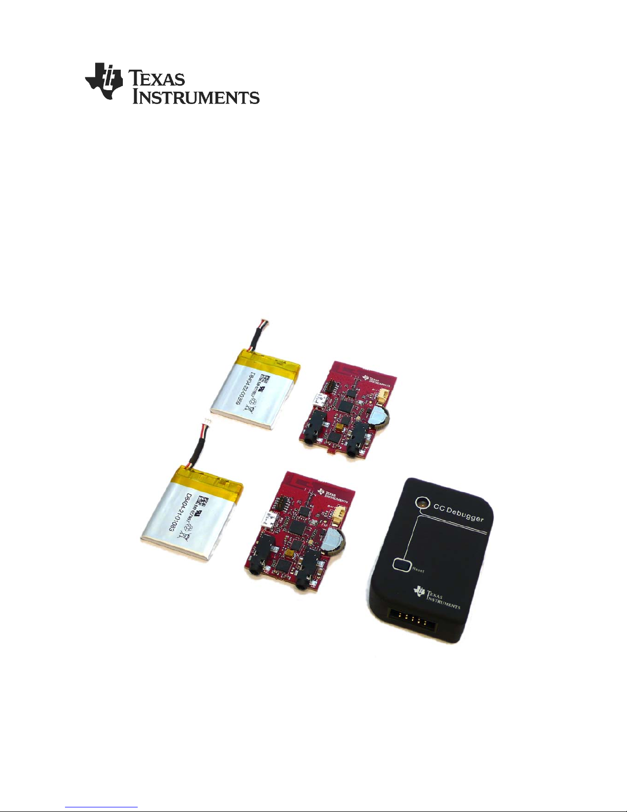
• 2 pcs CC85xx Headset boards
• 2 pcs 1.72Wh (3.7V, 465mAh) Li-ion batteries
• 1 pcs CC Debugger [7], used to program the CC8531 onboard the CC85xx Headset
boards, or in an end customer application
Figure 1. The main components included in the PurePath Wireless Headset Kit.
Also included in the kit is:
Page 6

A
www.ti.com
SWRU281A
Page 6 of 20
• 1 USB micro cable for charging the Li-ion battery and for powering the CC85xx Headset
boards.
• 1 audio cable (3.5mm jack to 3.5mm jack) to be used at the analog input.
• Documentation
Page 7
A
www.ti.com
SWRU281A
Page 7 of 20
5 Getting Started With the PurePath Wireless Headset Kit
The CC85xx Headset boards are pre-programmed in produc tion. This pre-programmed firmware
can be found in the example project “CC85XXDK-HEADSET Preloaded Demo” in the PurePath
Wireless Configurator [4]. The boards are labeled with MASTER and SLAVE stickers, and
instructions on how to pair them and start the audio streaming can be found in the CC85XXDKHEADSET Quick Start Guide [2]. Please note that when purchasing CC85xx devices they com e
un-programmed from production.
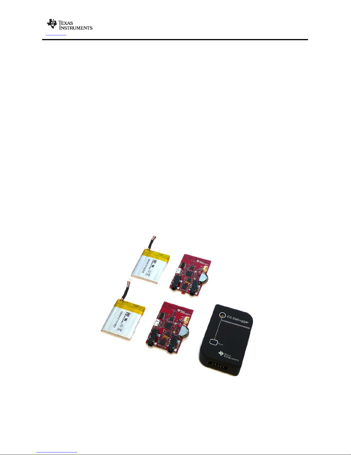
Figure 2 shows the main components of the CC85xx Headset board.
Figure 2. Photo of the CC85xx Headset board
The pre-programmed firmware on the two CC85xx Headset boards demonstrates a stereo input
base station (labeled MASTER) streaming audio to a stereo headphone (labeled SLAVE). The
main features of this pre-programmed application are:
• Uncompressed audio (PCM16)
• 44.1 kHz sample rate
Page 8
A
www.ti.com
SWRU281A
Page 8 of 20
• Maximum latency (2048 samples i.e. 46.44 ms with the 44.1 kHz sample rate)
• Optimized codec register settings in order to lower the power consumption
• Volume control on the slave using the UP and DOWN positions on the slave rocker switch
• Power ON/OFF on both master and slave by pressing the rocker switch IN for 1.6 sec.
• Pairing button on both master and slave by a fast press on the rocker switch IN
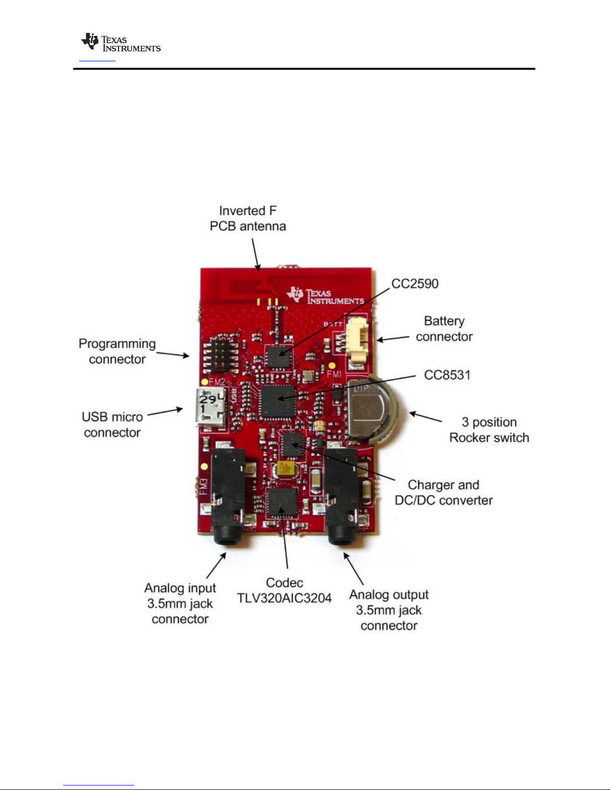
To change this functionality the CC85xx must be re-programmed. Figure 3 shows how to connect
the CC debugger to the CC85xx Headset board, which is used to program the CC85xx. The
CC85xx Headset board must be powered eit her with the battery or t he USB cable, in order for t he
CC Debugger to recognize the CC85xx. Further it’s important to place the programming connector
so that the red wire (pin 1) is oriented towards the USB connector as shown in the Figure 3. For
more details about the programming connector see section 6.6. If the board is powered and the CC
Debugger is connected correctly, pressing the reset button on the CC Debugger should make the
LED on the CC Debugger turn green. If so, the CC debugger is ready to download firmware
images from the PurePath Wireless Configurator.
The PurePath Wireless Configurator is used to configure the functionality of the CC85xx, and it can
be downloaded from the PurePath W ireless Configurator product page [4]. A screen shot of the
PurePath Wireless Configurator is shown in Figure 4.
Figure 3. CC debugger connected to the CC85xx Headset board
Page 9

A
www.ti.com
SWRU281A
Page 9 of 20
Figure 4 Screen shot of the PurePath Wireless Configurator.
6 Hardware Overview
This section describes each block of the CC85xx Headset board. A simplified block diagram of the
CC85xx Headset board is shown in Figure 5.
CC8531
BQ25015
Charger with Integrated
Synchronous Buck Converter
CC2590
(Range
Extender)
PAEN
EN
RF_N
RF_P
GIO14_xPAEN
GIO15_xLNAEN
RF_N
RF_P
TLV320AIC3204
(Low power codec)
GIO7_AD0
GIO8_AD1
GIO4_MCLK
GIO4_BCLK
GIO4_WCLK
GIO10_SCL
GIO11_SDA
GIO2_RESET
CSN
GIO9/I2S_AD2
GIO3
DIN
MCLK
SCLK
LRCLK
SCL
SDA
RESET
HPLOUT
2.1V
3.7V Li-Ion battery
(465mAh)
3.7V
DVDD
HPROUT
IN1L
IN1R
L
R
Charge indicator LED
Status LED
DOUT
USB Connector
USBP
USBM
VBUS (5V)
USBP
USBM
GIO3
Rocker Switch
PCB antenna
Mic/Line-in
Figure 5. Block diagram of the CC85xx Headset board.
Page 10

A
www.ti.com
SWRU281A
Page 10 of 20
6.1 TLV320AIC3204 Codec
The codec on the CC85xx Headset board is the TLV320AIC3204 [3] from Texas Instr uments Inc.
The TLV320AIC3204 is a stereo codec that supports six single-ended or 3 fully differential inputs.
On the CC85xx Headset board two input pins are used in single ended configuration (IN1L and
IN1R). The other inputs on the TLV320AIC3204 are unconnected. The TLV320AIC3204 has four
output pins. On the CC85xx Headset board two of these are used in single-ended configuration for
the headphone left and right. The other two outputs are unconnected.
The codec settings can be changed by changing the I
2
C configuration of the codec in the PurePath
Wireless Configurator. For more details on how to configure the codec, see the PurePath Wireless
Configurator help system. This is opened by selecting Help->Configurator Help in the PurePath
Wireless Configurator. For more details about the I
2
C interface available on the CC85xx see the
CC85xx Family User’s Guide [5].
Audio tests have been conducted to verify codec performance. The codec has been run with local
LDO enabled, running at 1.77V. THD+N and SNR tests were c onducted with a Rhode & Schwartz
UPA audio analyzer. The firmware used to measure the performance is the pre-programmed
firmware i.e., from the analog input of the Master to the analog output of the Slave. T he volume on
the slave must be maximized to reproduce these measurements. The measured SNR performance
a-weighted at 1 kHz input is approximately 93 dB. The THD+N is measured t o be approximately 83 dB at an input volt age of 250 mVrms.
6.2 Power supply and chargi ng of Li -ion ba t t e ry
The CC85xx Headset board can be powered from the following sources
- Li-ion battery included in the kit
- USB interface, micro-USB type
Onboard the CC85xx Headset board is a single-chip charger and DC/DC converter i.e. BQ25015
[8]. The output voltage from its switch mode regulator is 2.15V which powers the other components
on the board (CC8531, CC2590 and TLV320AIC3204). The current consumption will vary with
different RF environments (more retransmission of data) as well as the volume of the audio.
However, the slave consumes in average approximately 22mA when using moderate audio
volume. This is measured at the battery (i.e. 81mW) with the firmware pre-programmed in
production. The master consumes approximately 31 mA measured at the battery. In powerdown
the CC85xx headset board consumes less than 0,1 mA measured at the batter y
The BQ25015 is also used to charge the Li-ion battery. Charging occurs when both the battery and
the USB cable are connected. The CC85xx headset board can stream audio while the battery is
being charged. The power led D3 (see Appendix B) is lit when
• the USB cable is connected while the battery is not.
• the battery is charging (the LED is turned off when charging is complete).
The charge current in the BQ25015 is set to 100 mA. The charging time for the battery is
approximately 5.5h (CC85xx in power down while charging).
6.3 CC2590 Range Extender
As can be seen from Figure 2, the CC85xx Headset board has the CC2590 [9] m ounted on the
board. This is a 2.4 GHz range extender which works seamlessly together with all the CC85xx
family members. The CC2590 provides a PA for increased output power (up to +11 dBm) and an
LNA for improved receiver sensitivity (typically 4 dB with the CC85xx). The CC2590 is not
mandatory in a design with the CC85xx but can be utilized where increased range is needed.
Page 11
A
www.ti.com
SWRU281A
Page 11 of 20
6.4 Buttons and LEDs
On the CC85xx Headset board there is a rocker switch and 2 LEDs to be used for “human
interaction”. This switch actually has 5 positions i.e. IN, UP, DOWN, HALFWAY UP and HALFWAY
DOWN, but the positions HALFWAY UP and HALFWAY DOWN are not in use. This can also be
seen from the schematic (Appendix A). Table 1 shows the button positions and the signals they
assert, as well as out-of-the-box functionality tied to these signals.
Table 1: Human interaction signal mapping
Button position
CC85xx pin
Out-of-the-box functionality
IN
CSN
Pairing button and power toggling
UP
GIO1
Slave: volume up, Master: no function
DOWN GIO3 Slave: volume down, Master: no function
HALFWAY UP
NC - HALFWAY DOWN
NC
-
LED (D2) is connected to the CC85xx pin GIO12, and the intended usage of this diode is as a
network status LED. For details on how to configure the network LED please see the PurePath
Wireless Configurator [4]. The other LED (D3) is connected to the charger IC BQ25015 (for more
details see section 6.2).
6.5 RF Performance
The CC85xx Headset board does not have the output connected to a SMA connector, it is only
connected to an inverted F antenna. However, the output power measured into a 50 0hm load as
shown in Figure 6, is approximately 9 dBm. Please note that the supply voltage of the board is
approximately 2.15V. Note that to achieve maximum output power the supply voltage of the board
must be raised from 2.15V to 3.3V. This can be done by changing the ratio between the BQ25015
feedback resistors according to eq 8 in the BQ25015 datasheet [14]. The audio link is sustained for
input signals above -87dBm. Hence, a total link budget of 96 dB can be ar chived with the CC85xx
Headset board.
Finally, the design is pre-scanned for ETSI and FCC compliance, and the CC85xx Headset board
is suitable to fulfill these specifications.
Page 12

A
www.ti.com
SWRU281A
Page 12 of 20
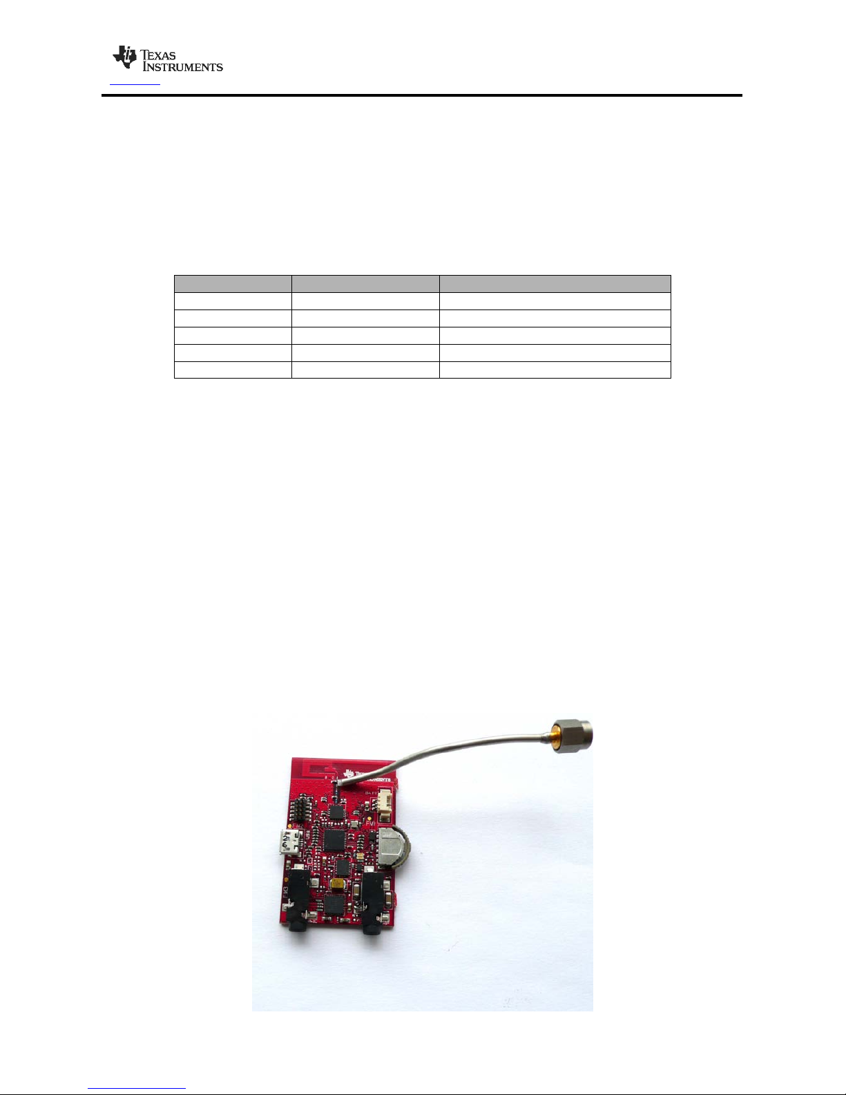
Figure 6. Photo of the CC85xx headset board connected to a 50ohm micro coax cable.
6.6 Programming Connect or
The Programming connector (see Figure 2) labeled DEBUG is used to program the CC85xx using
the CC Debugger. The pin-out of the programming interface is listed in Table 2. Figure 3 shows
how to connect the CC Debugger to the CC85xx Headset board. For more details about the CC
debugger, see the CC debugger product page [7].
The connector can also be used to connect an external MCU for controlling the CC85xx with the
external host interface. The pins needed for this are GND, CSn, SCLK, MISO, MOSI and RSTN.
For more details about the external host interface, see the CC85xx Family User ’s Guide [5]. Note
that the CC85xx Headset board needs to be powered by the battery or the USB while
programming.
Table 2: Program interface pin mapping
CC debugger pin
CC debugger Pin name
CC85xx pin
1 GND GND
2
Vdd from target
IOVDD
3
DC (Debug Clock)
NC
4
DD (Debug Data)
NC
5 CSn (SPI Chip Select) CSN
6
SCLK (SPI Clock)
SCLK
7
RESETn
RSTN
8
MOSI (SPI Data Out)
MOSI
9 3.3V Vdd (from debugger) NC
10
MISO (SPI Data In)
MISO
6.7 Test signals availabl e on P 7
Table 3 shows the signals available on the test pads on the back of the board.
Figure 7. Test pad 1
Page 13

A
www.ti.com
SWRU281A
Page 13 of 20
Table 3: Test signals (P7)
Test pad
number
Signal
1
GND
2
MCLK
3
WCLK
4
BCLK
5
DOUT
6
DIN
7
CODEC_RESET
8
I2C_SCL
9
NC
10
I2C_SDA
Page 14

A
www.ti.com
SWRU281A
Page 14 of 20
7 References
[1] Purepath Wireless Audio product page
http://www.ti.com/ww/en/analog/cc8520/index.shtml
[2] CC85XXDK-HEADSET Quick Start Guide
http://www.ti.com/lit/pdf/swru282
[3] TLV320AIC3204 Product folder:
http://focus.ti.com/docs/prod/folders/print/tlv320aic3204.html
[4] PurePath Wireless Configurator product page
http://focus.ti.com/docs/toolsw/folders/print/purepath-wl-cfg.html
[5] CC85xx Family User’s Guide
http://focus.ti.com/general/docs/lit/getliterature.tsp?baseLiteratureNumber=swru250
[6] CC8520 Product folder
http://focus.ti.com/docs/prod/folders/print/cc8520.html
[7] CC Debugger product page
http://focus.ti.com/docs/toolsw/folders/print/cc-debugger.html
[8] BQ25015 Product folder:
http://focus.ti.com/docs/prod/folders/print/bq25015.html
[9] CC2590 Product page
http://focus.ti.com/docs/prod/folders/print/cc2590.html
[10] CC85XXDK-HEADSET product page
http://focus.ti.com/docs/toolsw/folders/print/cc85xxdk-headset.html
[11] CC85XXDK-HEADSET reference design page
http://focus.ti.com/docs/toolsw/folders/print/cc85xxem-rd.html
[12] Texas Instruments Low Power RF forum
http://www.ti.com/lprf-forum
[13] Texas Instruments Support
http://support.ti.com
[14] BQ25015 Datasheet
http://focus.ti.com/lit/ds/symlink/bq25015.pdf
Page 15

A
www.ti.com
SWRU281A
Page 15 of 20
8 Document History
Revision
Date
Description/Changes
A
2011-03-31
Initial release
Page 16

A
www.ti.com
SWRU281A
Page 16 of 20
Appendix A: CC85xx Headset Schematic
Page 17

A
www.ti.com
SWRU281A
Page 17 of 20
Page 18

A
www.ti.com
SWRU281A
Page 18 of 20
Page 19

A
www.ti.com
SWRU281A
Page 19 of 20
Page 20

A
www.ti.com
SWRU281A
Page 20 of 20
Appendix B: CC85xx Headset Components Placement
Page 21

IMPORTANT NOTICE
Texas Instruments Incorporated and its subsidiaries (TI) reserve the right to make corrections, modifications, enhancements, improvements,
and other changes to its products and services at any time and to discontinue any product or service without notice. Customers should
obtain the latest relevant information before placing orders and should verify that such information is current and complete. All products are
sold subject to TI’s terms and conditions of sale supplied at the time of order acknowledgment.
TI warrants performance of its hardware products to the specifications applicable at the time of sale in accordance with TI’s standard
warranty. Testing and other quality control techniques are used to the extent TI deems necessary to support this warranty. Except where
mandated by government requirements, testing of all parameters of each product is not necessarily performed.
TI assumes no liability for applications assistance or customer product design. Customers are responsible for their products and
applications using TI components. To minimize the risks associated with customer products and applications, customers should provide
adequate design and operating safeguards.
TI does not warrant or represent that any license, either express or implied, is granted under any TI patent right, copyright, mask work right,
or other TI intellectual property right relating to any combination, machine, or process in which TI products or services are used. Information
published by TI regarding third-party products or services does not constitute a license from TI to use such products or services or a
warranty or endorsement thereof. Use of such information may require a license from a third party under the patents or other intellectual
property of the third party, or a license from TI under the patents or other intellectual property of TI.
Reproduction of TI information in TI data books or data sheets is permissible only if reproduction is without alteration and is accompanied
by all associated warranties, conditions, limitations, and notices. Reproduction of this information with alteration is an unfair and deceptive
business practice. TI is not responsible or liable for such altered documentation. Information of third parties may be subject to additional
restrictions.
Resale of TI products or services with statements different from or beyond the parameters stated by TI for that product or service voids all
express and any implied warranties for the associated TI product or service and is an unfair and deceptive business practice. TI is not
responsible or liable for any such statements.
TI products are not authorized for use in safety-critical applications (such as life support) where a failure of the TI product would reasonably
be expected to cause severe personal injury or death, unless officers of the parties have executed an agreement specifically governing
such use. Buyers represent that they have all necessary expertise in the safety and regulatory ramifications of their applications, and
acknowledge and agree that they are solely responsible for all legal, regulatory and safety-related requirements concerning their products
and any use of TI products in such safety-critical applications, notwithstanding any applications-related information or support that may be
provided by TI. Further, Buyers must fully indemnify TI and its representatives against any damages arising out of the use of TI products in
such safety-critical applications.
TI products are neither designed nor intended for use in military/aerospace applications or environments unless the TI products are
specifically designated by TI as military-grade or "enhanced plastic." Only products designated by TI as military-grade meet military
specifications. Buyers acknowledge and agree that any such use of TI products which TI has not designated as military-grade is solely at
the Buyer's risk, and that they are solely responsible for compliance with all legal and regulatory requirements in connection with such use.
TI products are neither designed nor intended for use in automotive applications or environments unless the specific TI products are
designated by TI as compliant with ISO/TS 16949 requirements. Buyers acknowledge and agree that, if they use any non-designated
products in automotive applications, TI will not be responsible for any failure to meet such requirements.
Following are URLs where you can obtain information on other Texas Instruments products and application solutions:
Products Applications
Audio www.ti.com/audio Communications and Telecom www.ti.com/communications
Amplifiers amplifier.ti.com Computers and Peripherals www.ti.com/computers
Data Converters dataconverter.ti.com Consumer Electronics www.ti.com/consumer-apps
DLP® Products www.dlp.com Energy and Lighting www.ti.com/energy
DSP dsp.ti.com Industrial www.ti.com/industrial
Clocks and Timers www.ti.com/clocks Medical www.ti.com/medical
Interface interface.ti.com Security www.ti.com/security
Logic logic.ti.com Space, Avionics and Defense www.ti.com/space-avionics-defense
Power Mgmt power.ti.com Transportation and www.ti.com/automotive
Microcontrollers microcontroller.ti.com Video and Imaging www.ti.com/video
RFID www.ti-rfid.com Wireless www.ti.com/wireless-apps
RF/IF and ZigBee® Solutions www.ti.com/lprf
TI E2E Community Home Page e2e.ti.com
Automotive
Mailing Address: Texas Instruments, Post Office Box 655303, Dallas, Texas 75265
Copyright © 2011, Texas Instruments Incorporated
 Loading...