

www.ti.com
查询PTV03020W供应商
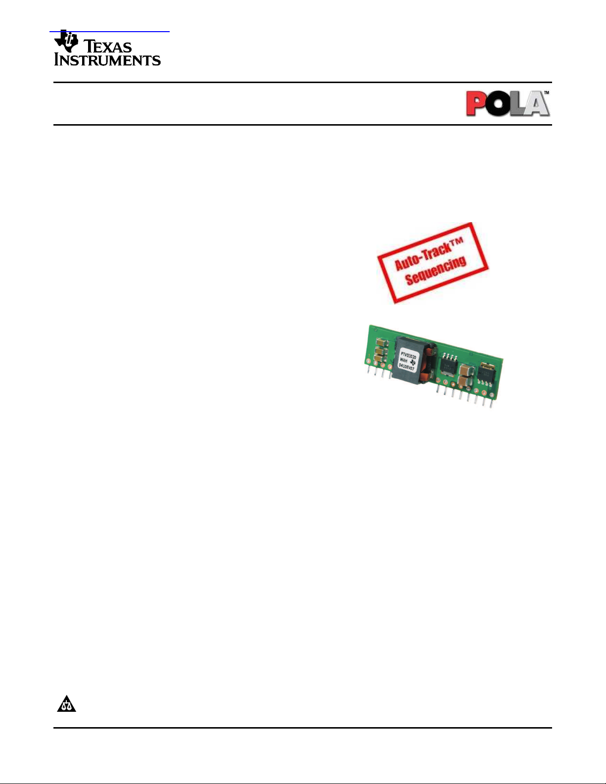
18-A, 3.3-V INPUT NONISOLATED WIDE-OUTPUT ADJUST SIP MODULE
FEATURES APPLICATIONS
• Up to 18-A Output Current
• 3.3-V Input Bus
• Wide-Output Voltage Adjust
(0.8 V to 2.5 V)
• Efficiencies up to 96%
• On/Off Inhibit
• Output Voltage Sense
• Prebias Start-Up
• Undervoltage Lockout
• Auto-Track™ Sequencing
• Output Overcurrent Protection (Nonlatching,
Auto-Reset)
• Overtemperature Protection
• Operating Temperature: –40 ° C to 85 ° C
• Safety Agency Approvals: UL/cUL 60950,
EN60950 VDE (Pending)
• POLA™ Compatible
• Multivoltage Digital Systems
• High-Density Logic Circuits
• High-End Computers and Servers
• 3.3-V Intermediate Bus Architectures
PTV03020W
SLTS243 – FEBRUARY 2005
DESCRIPTION
The PTV03020W is a ready-to-use nonisolated power module, and part of a new class of complete dc/dc
switching regulators from Texas Instruments. These regulators combine high performance with double-sided,
surface-mount construction, to give designers the flexibility to power the most complex multiprocessor digital
systems using off-the-shelf catalog parts.
The PTV03020W series is produced in a 12-pin, single in-line pin (SIP) package. The SIP footprint minimizes
board space, and offers an alternate package option for space conscious applications. Operating from a 3.3-V
input bus, the series provides step-down conversion to a wide range of output voltages, at up to 18 A of output
current. The output voltage can be set to any value over the range, 0.8 V to 2.5 V, using a single external
resistor.
This series includes Auto-Track™. Auto-Track simplifies the task of supply-voltage sequencing in a power
system by enabling the output voltage of multiple modules to accurately track each other, or any external voltage,
during power up and power down.
Other operating features include an on/off inhibit, and the ability to start up into an existing output voltage or
prebias. For improved load regulation, an output voltage sense is provided. A nonlatching overcurrent trip and
overtemperature shutdown protect against load faults.
Target applications include complex multivoltage, multiprocessor systems that incorporate the industry's
high-speed microprocessors, bus drivers, and the TMS320™ DSP family.
Please be aware that an important notice concerning availability, standard warranty, and use in critical applications of Texas
Instruments semiconductor products and disclaimers thereto appears at the end of this data sheet.
POLA, Auto-Track, TMS320 are trademarks of Texas Instruments.
PRODUCTION DATA information is current as of publication date.
Products conform to specifications per the terms of the Texas
Instruments standard warranty. Production processing does not
necessarily include testing of all parameters.
Copyright © 2005, Texas Instruments Incorporated
www.ti.com
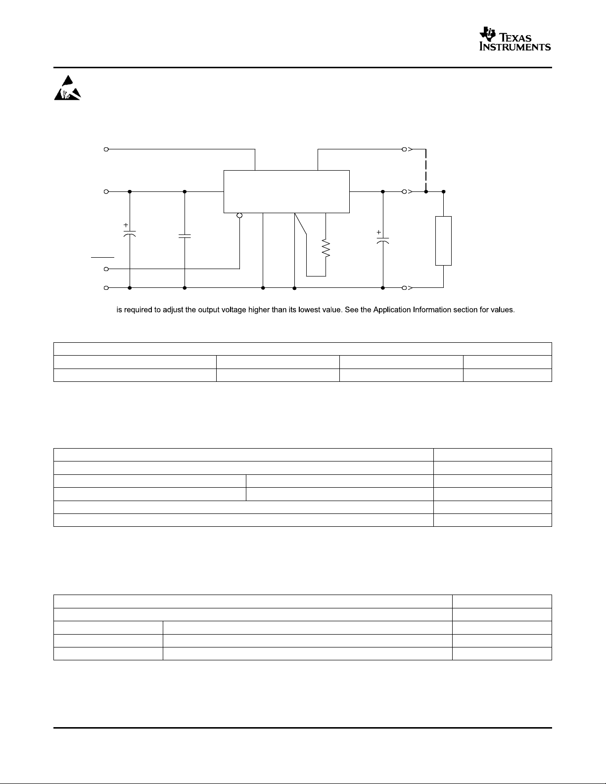
L
O
A
D
Track
GND
9 7
3, 4
81, 210, 11
12
5, 6
GND GNDInhibit
Track Sense
PTV03020W
Inhibit
V
I
V
I
V
O
V Adj
O
V
O
Sense
V
O
GND
C1*
680 Fm
(Required)
C2*
22 Fm
Ceramic
(Required)
C3*
330 Fm
(Optional)
R
SET
#
1%
0.05 W
(Required)
*
See the Application Information section for capacitor recommendations.
#
R
SET
PTV03020W
SLTS243 – FEBRUARY 2005
These devices have limited built-in ESD protection. The leads should be shorted together or the device
placed in conductive foam during storage or handling to prevent electrostatic damage to the MOS gates.
STANDARD APPLICATION
ORDERING INFORMATION
PTV03020 (Basic Model)
Output Voltage Part Number DESCRIPTION Package
0.8 V – 2.5 V (Adjustable) PTV03020WAH Vertical T/H EVC
(1) See the applicable package drawing for dimensions and PC board layout.
(1)
ABSOLUTE MAXIMUM RATINGS
over operating free-air temperature range unless otherwise noted
V
(Track)
T
A
T
stg
V
(INH)
(1) Stresses beyond those listed under absolute maximum ratings may cause permanent damage to the device. These are stress ratings
only, and functional operation of the device at these or any other conditions beyond those indicated under recommended operating
conditions is not implied. Exposure to absolute-maximum-rated conditions for extended periods may affect device reliability.
(2) This product is NOT compatible with surface-mount reflow solder processes.
Track input voltage –0.3 V to VI+0.3 V
Operating temperature range Over VIrange –40 ° C to 85 ° C
Lead temperature 5 seconds 260 ° C
Storage temperature –40 ° C to 125 ° C
Inhibit input voltage –0.3 V to VI+ 0.3 V
(1)
PACKAGE SPECIFICATIONS
PTV03020W (Suffix AH)
Weight 5.5 grams
Flammability Meets UL 94 V-O
Mechanical shock Per Mil-STD-883D, Method 2002.3, 1 ms, 1/2 sine, mounted 500 Gs
Mechanical vibration Mil-STD-883D, Method 2007.2, 20 Hz - 2000 Hz 10 Gs
(1) Qualification limit.
2
UNIT
(2)
(1)
(1)
www.ti.com
PTV03020W
SLTS243 – FEBRUARY 2005
ELECTRICAL CHARACTERISTICS
operating at 25 ° C free-air temperature, VI= 3.3 V, VO= 2.5 V, C1 = 680 µF, C2 = 22 µF, C3 = 0 µF, and IO= IOmax (unless
otherwise noted)
PARAMETER TEST CONDITIONS MIN TYP MAX UNIT
I
O
V
I
Output current Natural convection airflow 0 18
Input voltage range Over IOload range 2.95
(2)
Set-point voltage tolerance ± 2%
Temperature variation –40 ° C < TA< 85 ° C ± 0.5%
V
O
Line regulation Over VIrange ± 5 mV
Load regulation Over IOrange ± 5 mV
Total output variation Includes set-point, line, load, –40 ° C ≤ TA≤ 85 ° C ± 3
Adjust range Over VIrange 0.8 2.5 V
R
= 2.21 k Ω , VO= 2.5 V 95%
SET
R
= 5.49 k Ω , VO= 1.8 V 92%
SET
R
= 8.87 k Ω , VO= 1.5 V 90%
η Efficiency IO= 12 A
Output voltage ripple
(pk-pk)
20-MHz bandwidth 20 mV
SET
R
= 17.4 k Ω , VO= 1.2 V 88%
SET
R
= 36.5 k Ω , VO= 1 V 86%
SET
R
= Open, VO= 0.8 V 83%
SET
IO(trip) Overcurrent threshold Reset, followed by auto-recovery 35 A
1-A/µs load step, 50 to 100% IOmax, C3 = 330 µF
Transient response Recovery time 70 µs
Voover/undershoot 120 mV
Track control (pin 9)
UVLO Undervoltage lockout V
Inhibit control (pin 12) VILInput low voltage –0.2 0.6
IILInput low current Pin to GND –0.13 mA
Control slew-rate limit C3 ≤ C3 (max) 1 V/ms
VIincreasing 2.8 2.95
VIdecreasing 2.2 2.7
VIHInput high voltage VI– 0.5 Open
Referenced to GND V
IILInput low current Pin to GND –0.24 mA
II(stby) Input standby current Inhibit (pin 12) to GND, Track (pin 9) open 10 mA
ƒ
S
MTBF Reliability 5 106Hr
Switching frequency Over VIand IOranges 250 300 340 kHz
External input capacitance µF
External output capacitance
Capacitance value µF
(C3)
Nonceramic (C1) 680
Ceramic (C2) 22
Nonceramic 0 330
Ceramic 0 300
Equivalent series resistance (nonceramic) 4
(5)
(5)
(6)
(8)
Per Telcordia SR-332, 50% stress, TA= 40 ° C, ground
benign
(1)
3.6 V
(3)
(3)
(4)
(7)
11,000
A
%V
o
PP
m Ω
(1) See thermal derating curves for safe operating area (SOA), or consult factory for appropriate derating.
(2) The minimum input voltage is 2.95 V or VO+ 0.65 V, whichever is greater.
(3) The set-point voltage tolerance is affected by the tolerance and stability of R
tolerance of 1%, with 100 ppm/ ° C or better temperature stability.
. The stated limit is unconditionally met if R
SET
SET
(4) This control pin is pulled up to the input voltage, VI. If this input is left open circuit, the module will operate when input power is applied.
A small low-leakage (< 100 nA) MOSFET is recommended for control. For further information, consult the related application note.
(5) A 22-µF high-frequency ceramic capacitor and 680-µF electrolytic input capacitor are required for proper operation. The electrolytic
capacitor must be rated for 750 mArms minimum ripple current. Consult the Application Information for further guidance on capacitor
selection.
(6) An external output capacitor is not required for basic operation. Adding 330 µF of distributed capacitance at the load improves the
transient response.
(7) This is the calculated maximum. The minimum ESR limitation often results in a lower value. Consult the Application Information for
further guidance.
(8) This is the typical ESR for all the electrolytic (nonceramic) output capacitance. Use 7 m Ω as the minimum when using maximum-ESR
values to calculate.
has a
3
www.ti.com
50
60
70
80
90
100
0 3 6 9 12 15 18
Efficiency - %
I - Output Current - A
O
V = 2.5 V
O
V = 1.5 V
O
V = 0.8 V
O
V = 1 V
O
0 3 6 9 12 15 18
V - Output Ripple Voltage - mV
O PP
0
10
20
30
40
50
I - Output Current - A
O
V = 2.5 V
O
V = 1 V
O
V = 1.5 V
O
V = 0.8 V
O
2 0
3 0
4 0
50
6 0
70
8 0
9 0
0 3 6 9 12 15 18
Air Temperature - C
o
I - Output Current - A
O
400 LFM
200 LFM
100 LFM
Nat Conv
Air Flow
0 3 6 9 12 15 18
0
1
2
3
4
5
P - Power Dissipation - W
D
I - Output Current - A
O
V = 2.5 V
O
V = 0.8 V
O
PTV03020W
SLTS243 – FEBRUARY 2005
TYPICAL CHARACTERISTICS (3.3-V INPUT)
EFFICIENCY OUTPUT VOLTAGE RIPPLE
vs vs
OUTPUT CURRENT OUTPUT CURRENT
Figure 1. Figure 2.
POWER DISSIPATION TEMPERATURE DERATING
vs vs
OUTPUT CURRENT OUTPUT CURRENT
(9) (10)
(9) The electrical characteristic data has been developed from actual products tested at 25 ° C. This data is considered typical for the
converter. Applies to Figure 1 , Figure 2 , and Figure 3 .
(10) The temperature derating curves represent the conditions at which internal components are at or below the manufacturer's maximum
operating temperatures. The airflow direction is parallel to the long axis of the module. Derating limits apply to modules soldered directly
to a 100 mm x 100 mm double-sided PCB with 2 oz. copper. Applies to Figure 4 .
4
Figure 3. Figure 4.
www.ti.com
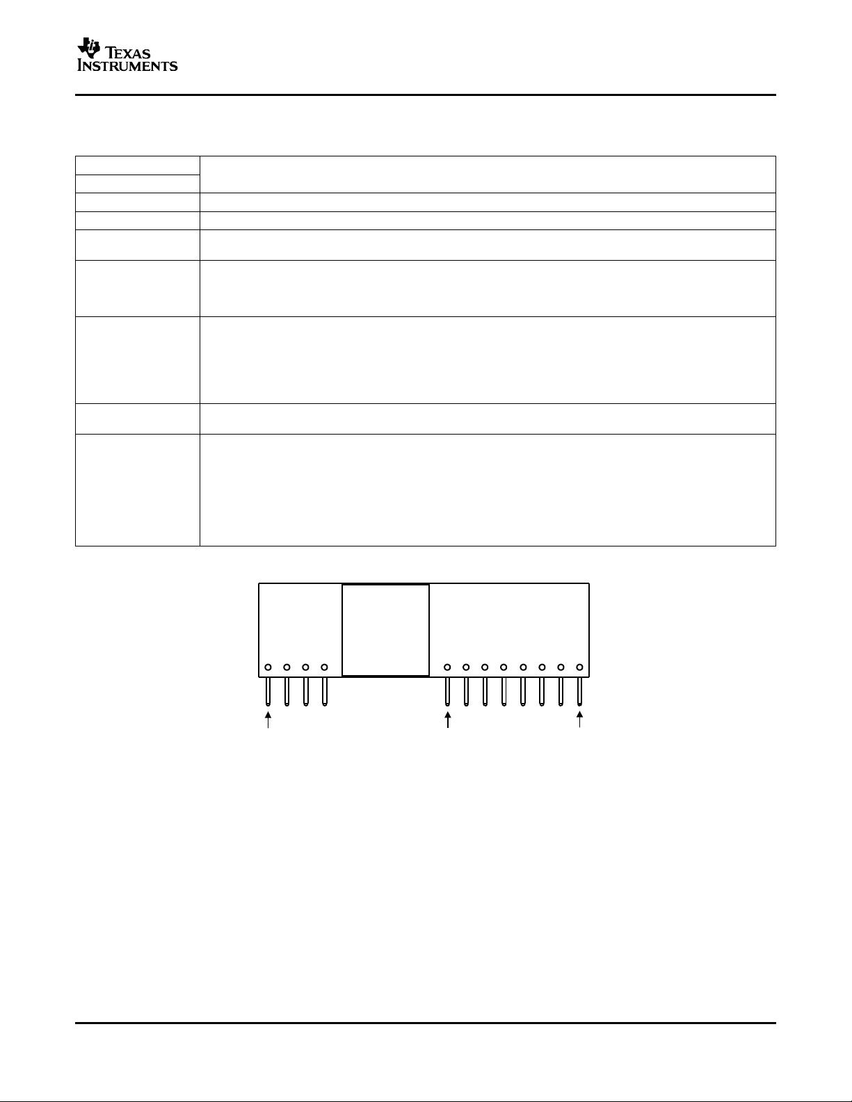
PIN 1 PIN 5
PIN 12
TERMINAL
NAME NO.
V
I
V
O
GND 1, 2, 10, 11
Inhibit 12
VoAdjust 8
VoSense 7
Track 9
5, 6 The positive input voltage power node to the module, which is referenced to common GND.
3, 4 The regulated positive power output with respect to the GND node.
PTV03020W
SLTS243 – FEBRUARY 2005
DEVICE INFORMATION
TERMINAL FUNCTIONS
DESCRIPTION
This is the common ground connection for the VIand VOpower connections. It is also the 0-Vdc reference for the
control inputs.
The Inhibit pin is an open-collector/drain, active-low input that is referenced to GND. Applying a low-level ground
signal to this input disables the module's output and turns off the output voltage. When the Inhibit control is active,
the input current drawn by the regulator is significantly reduced. If the inhibit feature is not used, the control pin
should be left open-circuit. The module then produces an output voltage whenever a valid input source is applied.
A 1% resistor must be connected directly between this pin and GND (pin 1 or 2) to set the output voltage of the
module higher than its lowest value. The temperature stability of the resistor should be 100 ppm/ ° C (or better).
The set-point range is 0.8 V to 3.6 V. The resistor value can be calculated using a formula. If this input is left
open-circuit, the output voltage defaults to its lowest value. For further information, consult the related application
note.
The specification table gives the standard resistor values for a number of common output voltages.
The sense input allows the regulation circuit to compensate for voltage drop between the module and the load. For
optimal voltage accuracy VoSense should be connected to VO. It can also be left disconnected.
This is an analog control input that enables the output voltage to follow an external voltage. This pin becomes
active typically 20 ms after the input voltage has been applied, and allows direct control of the output voltage from
0 V up to the nominal set-point voltage. Within this range, the output follows the voltage at the Track pin on a
volt-for-volt basis. When the control voltage is raised above this range, the module regulates at its set-point
voltage. The feature allows the output voltage to rise simultaneously with other modules powered from the same
input bus. If unused, this input should be connected to VI.
NOTE: Due to the undervoltage lockout feature, the output of the module cannot follow its own input voltage
during power up. Consult the related Application Information for further guidance.
Front View of Module
Figure 5. Pin Terminal Locations
5

www.ti.com
PTV03020W
SLTS243 – FEBRUARY 2005
APPLICATION INFORMATION
Capacitor Recommendations for the PTV03020W Power Module
Input Capacitors
The required input capacitors are a 22-µF ceramic and a minimum of 680-µF electrolytic type. For V
IO> 11 A , the 680-µF capacitance must be rated for 750 mArms ripple current capability. For all other
conditions, the ripple current rating must be at least 500 mArms. Where applicable, Table 1 gives the maximum
output voltage and current limits for a capacitor's rms ripple current rating.
The above ripple current requirements are conditional that the 22-µF ceramic capacitor is present. The 22-µF
X5R/X7R ceramic capacitor is necessary to reduce both the magnitude of ripple current through the electroytic
capacitor and the amount of ripple current reflected back to the input source. Ceramic capacitors should be
located within 0.5 inch. (1,3 cm) of the module's input pins. Additional ceramic capacitors can be added to reduce
the RMS ripple current requirement for the electrolytic capacitor.
Ripple current (Arms) rating, less than 100-m Ω equivalent series resistance (ESR), and temperature are the
major considerations when selecting input capacitors. Unlike polymer-tantalum capacitors, regular tantalum
capacitors have a recommended minimum voltage rating of 2 × (max. dc voltage + ac ripple). This is standard
practice to ensure reliability. Only a few tantalum capacitors were found to have sufficient voltage rating to meet
this requirement. At temperatures below 0 ° C, the ESR of aluminum electrolytic capacitors increases. For these
applications, Os-Con, polymer-tantalum, and polymer-aluminum types should be considered.
Output Capacitor (Optional)
For applications with load transients (sudden changes in load current), regulator response benefits from external
output capacitance. The recommended output capacitance of 330 µF allows the module to meet its transient
response specification. For most applications, a high-quality computer-grade aluminum electrolytic capacitor is
adequate. These capacitors provide decoupling over the frequency range, 2 kHz to 150 kHz, and are suitable
when ambient temperatures are above 0 ° C. For operation below 0 ° C, tantalum-, ceramic-, or Os-Con-type
capacitors are recommended. When using one or more nonceramic capacitors, the calculated equivalent ESR
should be no lower than 4 m Ω (7 m Ω using the manufacturer's maximum ESR for a single capacitor). A list of
preferred low-ESR-type capacitors are identified in Table 1 .
> 1 V and
O
Ceramic Capacitors
Above 150 kHz, the performance of aluminum electrolytic capacitors is less effective. Multilayer ceramic
capacitors have low ESR and a resonant frequency higher than the bandwidth of the regulator. They can be
used to reduce the reflected ripple current at the input as well as improve the transient response of the output.
When used on the output, their combined ESR is not critical as long as the total value of ceramic capacitance
does not exceed approximately 300 µF. Also, to prevent the formation of local resonances, do not place more
than five identical ceramic capacitors in parallel with values of 10 µF or greater.
Tantalum Capacitors
Tantalum-type capacitors can only be used on the output bus, and are recommended for applications where the
ambient operating temperature can be less than 0 ° C. The AVX TPS, Sprague 593D/594/595 and Kemet
T495/T510 capacitor series are suggested over many other tantalum types due to their higher rated surge, power
dissipation, and ripple current capability. As a caution, many general-purpose tantalum capacitors have
considerably higher ESR, reduced power dissipation, and lower ripple current capability. These capacitors are
also less reliable as they have reduced power dissipation and surge current ratings. Tantalum capacitors that
have no stated ESR or surge current rating are not recommended for power applications.
When specifying Os-con and polymer tantalum capacitors for the output, the minimum ESR limit is encountered
before the maximum capacitance value is reached.
Capacitor Table
Table 1 identifies the characteristics of capacitors from a number of vendors with acceptable ESR and ripple
current (rms) ratings. The recommended number of capacitors required at both the input and output buses is
identified for each capacitor type.
6

www.ti.com
PTV03020W
SLTS243 – FEBRUARY 2005
APPLICATION INFORMATION (continued)
Note: This is not an extensive capacitor list. Capacitors from other vendors are available with comparable
specifications. Those listed are for guidance. The RMS ripple current rating and ESR (at 100 kHz) are critical
parameters necessary to ensure both optimum regulator performance and long capacitor life.
Designing for Fast Load Transients
The transient response of the dc/dc converter has been characterized using a load transient with a di/dt of 1
A/µs. The typical voltage deviation for this load transient is given in the data sheet specification table using the
optional value of output capacitance. As the di/dt of a transient is increased, the response of a converter
regulation circuit ultimately depends on its output capacitor decoupling network. This is an inherent limitation with
any dc/dc converter once the speed of the transient exceeds its bandwidth capability. If the target application
specifies a higher di/dt or lower voltage deviation, the requirement can only be met with additional output
capacitor decoupling. In these cases special attention must be paid to the type, value, and ESR of the capacitors
selected.
If the transient performance requirements exceed that specified in the data sheet, or the total amount of load
capacitance is above 3000 µF, the selection of output capacitors becomes more important.
Table 1. Input/Output Capacitors
Capacitor Characteristics Quantity
Capacitor Vendor, Vendor
Type/Series (Style) Part Number
Panasonic, Aluminum 10 680 0.09 775 10 × 12.5 1 1 EEUFC1E681
WA(SMD) 6.3 680 0.015 5100 10 × 10.2 1 1 EEFWA0J681P
FK (SMD) 16 680 0.08 850 10 × 10.2 1 1 EEVFK1C681P
United Chemi-Con
PSA,Poly- Aluminum (Radial) 6.3 680 0.007 5860 10 × 11.5 1 ≤ 1 PSA6.3VB680MJ11
LXZ, Aluminum (Radial) 10 680 0.09 760 10 × 12.5 1 1 LXZ10VB681M10X12LL
PS, Poly-Aluminum (Radial) 6.3 680 0.01 5500 10 × 12.5 1 ≤ 2 6PS680MJ12
PXA, Poly-Aluminum (SMD) 6.3 680 0.01 5500 10 × 12.2 1 ≤ 2 PXA6.3VC681MJ12TP
Nichicon, Aluminum 10 680 0.09 1060 12.5 × 15 1 1 UPM1A681MHH6
HD (Radial) 10 680 0.053 1030 10 × 12.5 1 1 UHD1A681MHR
Panasonic, Poly-Aluminum
WA (SMD) 16 330 0.022 4100 10 × 10.2 2
S/SE (SMD)Poly-Tanalum 6.3 180 0.005 4000 7.3 × 154.3 × 4.2 N/R
Sanyo
TP, Poscap 10 330 0.025 3000 7.3 L × 4.3 W 2
SP, Os-Con 6.3 680 0.013 >4800 10 × 10.5 1 ≤ 2 6SP680M
SVP, Os-Con (SMD) 6.3 820 0.012 5400 11 × 12.7 1 ≤ 2 6SVP820M
AVX, Tantalum, Series III 10 330 0.06 >1723 2 ≤ 5 TPSV337M010R0060
TPS (SMD) 10 330 0.04 >2200 2 ≤ 5 TPSE337M010R0040
Kemet (SMD)
T520, Poly-Tant 10 330 0.04 1800 2 ≤ 5 T520X337M010AS
T530, Poly-Tant/Organic 10 330 0.01 >3800 43 W × 7.3 L × 4 H 2 ≤ 1 T530X337M010ASE010
Vishay-Sprague 6.3 820 0.014 5040 11 × 12 1 ≤ 2 94SVP827X06R3F12
94SVP,(Oscon)(SMD)
595D, Tantalum (SMD) 10 680 0.09 1680 7.2 L × 6 W × 4.1 H 1 ≤ 5 595D687X0010R2T
94SA, Os-Con (Radial) 6.3 680 0.013 4840 10 × 10.5 1 ≤ 2 94SA687X06R3FBP
Kemet, Ceramic X5R (SMD) 16 10 0.002 — 3225 ≥ 2
Working Max ESR Optional
Voltage at 100 kHz Output
Value Current at Physical Size Input
(V) ( Ω ) Bus
6.3 470 0.01 4200 2 ≤ 1 T530X477M006ASE010
6.3 22 0.002 3225 ≥ 1
(µF) 85 ° C (Irms) (mm) Bus
Max Ripple
(mA)
(1)
(1)
7.3L × 5.7 W × 4.1 H
≤ 3 EEFWA1C331P
(2)
≤ 1 EEFSE0J181R
≤ 4 10TPE330M
(3)
≤ 5 C1210C106M4PAC
(3)
≤ 5 C1210C226K9PAC
(1) Total capacitance of 660 µF is acceptable based on the combined ripple current rating.
(2) N/R – Not recommended. The voltage rating does not meet the minimum operating limits.
(3) Ceramic capacitors are required to complement electrolytic types at the input and to reduce high-frequency ripple current.
7

www.ti.com
R = 10 k x
SET
W
0.8 V
V - 0.8 V
O
= 2.49 kW
PTV03020W
SLTS243 – FEBRUARY 2005
APPLICATION INFORMATION (continued)
Table 1. Input/Output Capacitors (continued)
Capacitor Characteristics Quantity
Capacitor Vendor, Vendor
Type/Series (Style) Part Number
Kemet, Ceramic X5R (SMD) 6.3 47 0.002 3225 ≥ 1
Murata, Ceramic X5R (SMD) 6.3 100 0.002 — 3225 ≥ 1
TDK, Ceramic X5R (SMD) 6.3 100 0.002 — 3225 ≥ 1
Working Max ESR Optional
Voltage at 100 kHz Output
Value Current at Physical Size Input
(V) ( Ω ) Bus
6.3 47 ≥ 1
6.3 47 ≥ 1
(µF) 85 ° C (Irms) (mm) Bus
16 22 ≥ 1
16 10 ≥ 2
16 22 ≥ 1
16 10 ≥ 2
Adjusting the Output Voltage
The V
to 2.5 V. The adjustment method requires the addition of a single external resistor, R
directly between the V
voltage is set to its lowest value. Table 2 gives the preferred value of the external resistor for a number of
standard voltages, along with the actual output voltage that this resistance value provides. Figure 6 shows the
placement of the required resistor.
Adjust control (pin 8) sets the output voltage of the PTV03020W product to a value over the range, 0.8 V
O
Adjust and the regulator's output GND (pin 1 or 2). Without an adjust resistor, the output
O
Max Ripple
(mA)
(3)
≤ 5 C1210C476K9PAC
(3)
≤ 3 GRM32ER60J107M
(3)
≤ 5 GRM32ER60J476M
(3)
≤ 5 GRM32ER61C226K
(3)
≤ 5 GRM32DR61C106K
(3)
≤ 3 C3225X5R0J107MT
(3)
≤ 5 C3225X5R0J476MT
(3)
≤ 5 C3225X5R1C226MT
(3)
≤ 5 C3225X5R1C106MT
, that must be connected
SET
Table 2. Nearest Standard Values of R
V
O
(Required) (Standard Value) (Actual)
(1)
2.5 V
R
SET
2.21 k Ω 2.502 V
for Common Output Voltages
SET
V
O
2 V 4.12 k Ω 2.010 V
1.8 V 5.49 k Ω 1.803 V
1.5 V 8.87 k Ω 1.504 V
1.2 V 17.4 k Ω 1.202 V
1 V 36.5 k Ω 1.005 V
0.8 V Open 0.800 V
(1) For VO=2.5 V, the minimum input voltage is 3.15 V. See Electrical Characteristics for additional
information.
For other output voltages, the value of the required resistor can either be calculated or simply selected from the
range of values given in Table 3 . Equation 1 may be used for calculating the adjust resistor value.
(1)
8

www.ti.com
PTV03020W
GND
V
O
V Adj
O
GND
V Sense
O
V
O
R , 1%
SET
GND
C
O
PTV03020W
SLTS243 – FEBRUARY 2005
Figure 6. V
Table 3. Calculated Values of R
V
O
Adjust Resistor Placement
O
for Other Output Voltages
SET
R
SET
V
O
0.800 Open 1.450 9.82 k Ω
0.825 318 k Ω 1.500 8.94 k Ω
0.850 158 k Ω 1.550 8.18 k Ω
0.875 104 k Ω 1.600 7.51 k Ω
0.900 77.5 k Ω 1.650 6.92 k Ω
0.925 61.5 k Ω 1.700 6.40 k Ω
0.950 50.8 k Ω 1.750 5.93 k Ω
0.975 43.2 k Ω 1.800 5.51 k Ω
1.000 37.5 k Ω 1.850 5.13 k Ω
1.025 33.1 k Ω 1.900 4.78 k Ω
1.050 29.5 k Ω 1.950 4.47 k Ω
1.075 26.6 k Ω 2.000 4.18 k Ω
1.100 24.2 k Ω 2.050 3.91 k Ω
1.125 22.1 k Ω 2.100 3.66 k Ω
1.150 20.4 k Ω 2.150 3.44 k Ω
1.175 18.8 k Ω 2.200 3.22 k Ω
1.200 17.5 k Ω 2.250 3.03 k Ω
1.225 16.3 k Ω 2.300 2.84 k Ω
1.250 15.3 k Ω 2.350
1.300 13.5 k Ω 2.400
1.350 12.1 k Ω 2.450
1.400 10.8 k Ω 2.500
(1)
(1)
(1)
(1)
(1) For VO> 2.3 V, the minimum required input voltage is VO+ 0.65 V. See the Electrical Characteristics
for additional information.
R
2.67 k Ω
2.51 k Ω
2.36 k Ω
2.22 k Ω
SET
9

www.ti.com
3.3 V
5, 6
9
7
3, 4
81, 210, 11
C1
680 Fm
+
C3
330 Fm
+
GND
GND
1.8 V
R
5.49 k
1%, 0.05 W
SET
W
C2
22 Fm
PTV03020W
Track
V
I
V
O
GND
Sense
Adjust
GND
L
O
A
D
t - Time = 5 ms/div
I (5 A/div)
I
V (1 V/div)
O
V (2 V/div)
I
PTV03020W
SLTS243 – FEBRUARY 2005
Features of the PTH/PTV Family of Nonisolated, Wide-Output Adjust Power Modules
POLA™ Compatibility
The PTH/PTV family of nonisolated, wide-output adjustable power modules from Texas Instruments are
optimized for applications that require a flexible, high-performance module that is small in size. Each of these
products are POLA™ compatible. POLA-compatible products are produced by a number of manufacturers, and
offer customers advanced, non-isolated modules with the same footprint and form factor. POLA parts are also
ensured to be interoperable, thereby providing customers with true second-source availability.
Soft-Start Power Up
The Auto-Track feature allows the power up of multiple PTH/PTV modules to be directly controlled from the
Track pin. However, in a stand-alone configuration, or when the Auto-Track feature is not being used, the Track
pin should be directly connected to the input voltage, Vi(see Figure 7 ).
Figure 7. Power-Up Application Circuit
When the Track pin is connected to the input voltage, the Auto-Track function is permanently disengaged. This
allows the module to power up entirely under the control of its internal soft-start circuitry. When power up is
under soft-start control, the output voltage rises to the set-point at a quicker and more linear rate.
Figure 8. Power-Up Waveform
10

www.ti.com
V
I
L
O
A
D
1 = Inhibit
GND
GND
V
O
V Sense
O
Q1
BSS138
R
SET
5.49 kW
C1 C3C2
PTV03020W
V
I
V
O
GND
GND
Inhibit
V Adj
O
Track Sense
PTV03020W
SLTS243 – FEBRUARY 2005
From the moment a valid input voltage is applied, the soft-start control introduces a short time delay (typically
less than 5 ms) before allowing the output voltage to rise. The output then progressively rises to the module
set-point voltage. Figure 8 shows the soft-start power-up characteristic of the PTV03020W, operating from a
3.3-V input bus and configured for a 1.8-V output. The waveforms were measured with a 5-A resistive load and
the Auto-Track feature disabled. The initial rise in input current when the input voltage first starts to rise is the
charge current drawn by the input capacitors. Power up is complete within 25 ms.
Output On/Off Inhibit
For applications requiring output voltage on/off control, the modules incorporate an output Inhibit control pin. The
inhibit feature can be used wherever there is a requirement for the output voltage from the regulator to be turned
off.
The power modules function normally when the Inhibit input is left open-circuit, providing a regulated output
whenever a valid source voltage is connected to VIwith respect to GND.
Figure 9 shows the typical application of the inhibit function. Note the discrete transistor (Q1). The Inhibit input
has its own internal pullup (see footnotes to electrical characteristics table). The input is not compatible with TTL
logic devices. An open-collector (or open-drain) discrete transistor is recommended for control.
Figure 9. On/Off Inhibit Application Circuit
Turning Q1 on applies a low voltage to the Inhibit control and disables the output of the module. If Q1 is then
turned off, the module executes a soft-start power-up sequence. A regulated output voltage is produced within 25
ms. Figure 10 shows the typical rise in both the output voltage and input current, following the turnoff of Q1. The
turnoff of Q1 corresponds to the rise in the waveform, Q1 V
constant current load.
. The waveforms were measured with a 9-A
DS
11

www.ti.com
t - Time = 5 ms/div
Q1 V (5 V/div)
DS
I (5 A/div)
I
V (1 V/div)
O
PTV03020W
SLTS243 – FEBRUARY 2005
Figure 10. Inhibit Waveform
Overcurrent Protection (OCP)
For protection against load faults, the modules incorporate output overcurrent protection. Applying a load that
exceeds the overcurrent threshold causes the regulated output to shut down. Following shutdown, a module
periodically attempts to recover by initiating a soft-start power up. This is described as a hiccup mode of
operation, whereby the module continues in the cycle of successive shutdown and power up until the load fault is
removed. During this period, the average current flowing into the fault is significantly reduced. Once the fault is
removed, the module automatically recovers and returns to normal operation.
Overtemperature Protection (OTP)
An onboard temperature sensor protects the module internal circuitry against excessively high temperatures. A
rise in the internal temperature may be the result of a drop in airflow or a high ambient temperature. If the
internal temperature exceeds the OTP threshold, the module Inhibit control is internally pulled low. This turns the
output off. The output voltage drops as the external output capacitors are discharged by the load circuit. The
recovery is automatic, and begins with a soft-start power up. It occurs when the sensed temperature decreases
by about 10 ° C below the trip point.
Note: The overtemperature protection is a last resort mechanism to prevent thermal stress to the regulator.
Operation at or close to the thermal shutdown temperature is not recommended and reduces the long-term
reliability of the module. Always operate the regulator within the specified Safe Operating Area (SOA) limits for
the worst-case conditions of ambient temperature and airflow.
Auto-Track™ Function
The Auto-Track function is unique to the PTH/PTV family, and is available with all POLA products. Auto-Track
was designed to simplify the amount of circuitry required to make the output voltage from each module power up
and power down in sequence. The sequencing of two or more supply voltages during power up is a common
requirement for complex mixed-signal applications that use dual-voltage VLSI ICs such as DSPs,
microprocessors, and ASICs.
How Auto-Track™ Works
Auto-Track works by forcing the module output voltage to follow a voltage presented at the Track control pin
This control range is limited to between 0 V and the module set-point voltage. Once the track-pin voltage is
raised above the set-point voltage, the module's output remains at its set-point
(2)
. As an example, if the Track
pin of a 1.8-V regulator is at 1 V, the regulated output is 1 V. But if the voltage at the Track pin rises to 3 V, the
regulated output does not go higher than 1.8 V.
(1)
.
12

www.ti.com
PTV03020W
SLTS243 – FEBRUARY 2005
When under Auto-Track control, the regulated output from the module follows the voltage at its Track pin on a
volt-for-volt basis. By connecting the Track pin of a number of these modules together, the output voltages follow
a common signal during power up and power down. The control signal can be an externally generated master
ramp waveform, or the output voltage from another power supply circuit
incorporates an internal RC-charge circuit. This operates off the module input voltage to produce a suitable rising
waveform at power up.
Typical Application
The basic implementation of Auto-Track allows for simultaneous voltage sequencing of a number of Auto-Track
compliant modules. Connecting the Track control pins of two or more modules forces the Track control of all
modules to follow the same collective RC-ramp waveform, and allows them to be controlled through a single
transistor or switch; see Q1 in Figure 11 .
To initiate a power-up sequence, it is recommended that the Track control first be pulled to ground potential. This
is done at or before input power is applied to the modules, and then held for at least 10 ms thereafter. This brief
period gives the modules time to complete their internal soft-start initialization. Applying a logic level high signal
to the circuit On/Off Control turns Q1 on and applies a ground signal to the Track input of the modules. After
completing their internal soft-start intialization, the output of all modules remains at zero volts while Q1 is on.
Q1 may be turned off 10 ms after a valid input voltage has been applied to the modules. This allows the track
control voltage to automatically rise to the module input voltage. During this period, the output voltage of each
module rises in unison with other modules to its respective set-point voltage.
Figure 12 shows the output voltage waveforms from the circuit of Figure 11 after the On/Off Control is set from a
high-level to a low-level voltage. The waveforms, VO1 and VO2 represent the output voltages from the two power
modules, U1 (2.5 V) and U2 (1.5 V), respectively. VO1 and VO2 are shown rising together to produce the desired
simultaneous power-up characteristic.
The same circuit also provides a power-down sequence. Power down is the reverse of power up, and is
accomplished by lowering the track control voltage back to zero volts. The important constraint is that a valid
input voltage must be maintained until the power down is complete. It also requires that Q1 be turned off
relatively slowly. This is so that the Track control voltage does not fall faster than Auto-Track slew rate capability,
which is 1 V/ms. The components R1 and C1 in Figure 11 limit the rate at which Q1 pulls down the Track control
voltage. The values of 100 k Ω and 0.1 µF correlate to a decay rate of about 0.17 V/ms.
The power-down sequence is initiated with a low-to-high transition at the On/Off Control input to the circuit.
Figure 13 shows the power-down waveforms. As the Track control voltage falls below the nominal set-point
voltage of each power module, then its output voltage decays with all the other modules under Auto-Track
control.
(3)
. For convenience, the Track input
Notes on Use of Auto-Track™
1. The Track pin voltage must be allowed to rise above the module set-point voltage before the module can
regulate at its adjusted set-point voltage.
2. The Auto-Track function tracks almost any voltage ramp during power up, and is compatible with ramp
speeds of up to 1 V/ms.
3. The absloute maximum voltage that may be applied to the Track pin is the input voltage VI.
4. The module cannot follow a voltage at its Track control input until it has completed its soft-start initialization.
This takes about 10 ms from the time that a valid voltage has been applied to its input. During this period, it
is recommended that the Track pin be held at ground potential.
5. The module is capable of both sinking and sourcing current when following a voltage at its Track input.
Therefore, start up into an output prebias cannot be supported when a module is under Auto-Track control.
Note: A prebias holdoff is not necessary when all supply voltages rise simultaneously under the control of
Auto-Track.
6. The Auto-Track function can be disabled by connecting the Track pin to the input voltage (V
Auto-Track is disabled, the output voltage rises at a quicker and more linear rate after input power has been
applied.
). When
I
13

www.ti.com
C4
+
C7
+
C2 C3
+
C5 C6
+
V 1 = 2.5 V
O
V 2 = 1.5 V
O
U1
U2
3.3 V
0 V
On/Off Control
1 = Power Down
0 = Power Up
Q1
BSS138
C1
0. 1 µF
R1
100 kW
R2
2.21 kW
R3
8.87 kW
PTV03020W
Track
V
I
V
O
GND
Sense
Adjust
GND
7
PTV03010W
V
I
GNDInhibit
Inhibit
V Adj
O
Track
V
O
t - Time = 10 ms/Div
V 1 (1 V/Div)
O
V 2 (1 V/Div)
O
On/Off Input (5 V/Div)
t - Time = 10 ms/Div
On/Off Input (5 V/Div)
V 2 (1 V/Div)
O
V 1 (1 V/Div)
O
PTV03020W
SLTS243 – FEBRUARY 2005
Figure 11. Sequenced Power Up and Power Down Using Auto-Track
Prebias Start-Up Capability
A prebias start-up condition occurs as a result of an external voltage being present at the output of a power
module prior to its output becoming active. This often occurs in complex digital systems when current from
another power source is backfed through a dual-supply logic component, such as an FPGA or ASIC. Another
path might be via clamp diodes, sometimes used as part of a dual-supply power-up sequencing arrangement. A
prebias can cause problems with power modules that incorporate synchronous rectifiers. This is because under
most operating conditions, such modules can sink as well as source output current. The PTH/PTV modules
incorporate synchronous rectifiers but do not sink current during start-up, or whenever the Inhibit pin is held low.
Start-up includes an initial delay (approximately 8–15 ms), followed by the rise of the output voltage under the
control of the module internal soft-start mechanism; see Figure 14 .
14
Figure 12. Simultaneous Power Up With Auto-Track Figure 13. Simultaneous Power Down With Auto-Track
Control Control

www.ti.com
t - Time = 10 ms/div
Start-Up
Period
V (1 V/div)
O
V (1 V/div)
I
t - Time = 10 ms/div
I (5 A/div)
O
V (1 V/div)
O
V (1 V/div)
I
PTV03020W
SLTS243 – FEBRUARY 2005
Conditions for Prebias Holdoff
In order for the module to allow an output prebias voltage to exist (and not sink current), certain conditions must
be maintained. The module holds off a prebias voltage when the Inhibit pin is held low, and whenever the output
is allowed to rise under soft-start control. Power up under soft-start control occurs on the removal of the ground
signal to the Inhibit pin (with input voltage applied), or when input power is applied with Auto-Track disabled
further ensure that the regulator does not sink output current (even with a ground signal applied to its Inhibit), the
input voltage must also be greater than the applied prebias source, throughout the power-up sequence
The soft-start period is complete when the output begins rising above the prebias voltage. The module then
functions as normal, and sinks current if a voltage higher than its set-point value is applied to its output.
Note: If a prebias condition is not present, the soft-start period is complete when the output voltage has risen to
either the set-point voltage, or the voltage applied at the module Track control pin, whichever is lowest.
Demonstration Circuit
Figure 15 shows the start-up waveforms for the demonstration circuit shown in Figure 16 . The initial rise in V
the prebias voltage, which is passed from the VCCIO to the VCORE voltage rail through the ASIC. Note that the
output current from the module (IO) is negligible until its output voltage rises above the applied prebias.
(1)
(2)
.
. To
is
O
Figure 14. PTV03020W Start-Up Figure 15. Prebias Start-Up Waveforms
NOTES:
1. The prebias start-up feature is not compatible with Auto-Track. If the rise in the output is limited by the
voltage applied to the Track control pin, the output sinks current during the period that the track control
voltage is below that of the back-feeding source. For this reason, Auto-Track should be disabled when not
being used. This is accomplished by connecting the Track pin to the input voltage, VI. This raises the Track
pin well above the set-point voltage prior to start-up, thereby defeating the Auto-Track feature.
2. To further ensure that the regulator output does not sink current when power is first applied (even with a
ground signal applied to the Inhibit control input), the input voltage must always be greater than the applied
prebias source. This condition must exist throughout the power-up sequence of the power system.
15

www.ti.com
V = 1.5 V
O
V = 3.3 V
I
R
8.87 k
SET
W
ASIC
VCORE
VCCIO
I
O
PTV03020W
Track
V
I
V
O
GND
Vadj
Sense
+
C1
+
C3
+
C2
PTV03020W
SLTS243 – FEBRUARY 2005
Figure 16. Application Circuit Demonstrating Prebias Start-Up
Output Remote Sense
Products with this feature incorporate an output voltage sense input, V
Sense. A remote sense improves the
O
load regulation performance of the module by allowing it to compensate for any remote IR voltage drop between
its output and the load. An IR drop is caused by the output current flowing through the small amount of pin and
trace resistance.
To use this feature, simply connect V
standard application). If the V
Sense input is left open-circuit, an internal low-value resistor (15 Ω or less)
O
Sense to the V
O
node, close to the load circuit (see the data sheet
O
connected between the pin and the output node, ensures that the output remains in regulation.
With the sense input connected, the difference between the voltage measured directly between the V
pins, and that measured from V
Sense to GND, is the amount of IR drop being compensated by the regulator.
O
This should be limited to a maximum of 0.3 V.
Note: The remote sense feature is not designed to compensate for the forward drop of nonlinear or frequency
dependent components that may be placed in series with the output. Examples include OR-ing diodes, filter
inductors, ferrite beads, and fuses. When these components are enclosed by the remote sense connection, they
are effectively placed inside the regulation control loop, which can adversely affect the stability of the module.
16
and GND
O

PACKAGE OPTION ADDENDUM
www.ti.com
12-Jan-2006
PACKAGING INFORMATION
Orderable Device Status
PTV03020WAH ACTIVE SIP MOD
(1)
Package
Type
Package
Drawing
Pins Package
Qty
Eco Plan
EVC 12 40 Pb-Free
ULE
(1)
The marketing status values are defined as follows:
ACTIVE: Product device recommended for new designs.
LIFEBUY: TI has announced that the device will be discontinued, and a lifetime-buy period is in effect.
NRND: Not recommended for new designs. Device is in production to support existing customers, but TI does not recommend using this part in
a new design.
PREVIEW: Device has been announced but is not in production. Samples may or may not be available.
OBSOLETE: TI has discontinued the production of the device.
(2)
Eco Plan - The planned eco-friendly classification: Pb-Free (RoHS), Pb-Free (RoHS Exempt), or Green (RoHS & no Sb/Br) - please check
http://www.ti.com/productcontent for the latest availability information and additional product content details.
TBD: The Pb-Free/Green conversion plan has not been defined.
Pb-Free (RoHS): TI's terms "Lead-Free" or "Pb-Free" mean semiconductor products that are compatible with the current RoHS requirements
for all 6 substances, including the requirement that lead not exceed 0.1% by weight in homogeneous materials. Where designed to be soldered
at high temperatures, TI Pb-Free products are suitable for use in specified lead-free processes.
Pb-Free (RoHS Exempt): This component has a RoHS exemption for either 1) lead-based flip-chip solder bumps used between the die and
package, or 2) lead-based die adhesive used between the die and leadframe. The component is otherwise considered Pb-Free (RoHS
compatible) as defined above.
Green (RoHS & no Sb/Br): TI defines "Green" to mean Pb-Free (RoHS compatible), and free of Bromine (Br) and Antimony (Sb) based flame
retardants (Br or Sb do not exceed 0.1% by weight in homogeneous material)
(RoHS)
(2)
Lead/Ball Finish MSL Peak Temp
Call TI N / A for Pkg Type
(3)
(3)
MSL, Peak Temp. -- The Moisture Sensitivity Level rating according to the JEDEC industry standard classifications, and peak solder
temperature.
Important Information and Disclaimer:The information provided on this page represents TI's knowledge and belief as of the date that it is
provided. TI bases its knowledge and belief on information provided by third parties, and makes no representation or warranty as to the
accuracy of such information. Efforts are underway to better integrate information from third parties. TI has taken and continues to take
reasonable steps to provide representative and accurate information but may not have conducted destructive testing or chemical analysis on
incoming materials and chemicals. TI and TI suppliers consider certain information to be proprietary, and thus CAS numbers and other limited
information may not be available for release.
In no event shall TI's liability arising out of such information exceed the total purchase price of the TI part(s) at issue in this document sold by TI
to Customer on an annual basis.
Addendum-Page 1


IMPORTANT NOTICE
Texas Instruments Incorporated and its subsidiaries (TI) reserve the right to make corrections, modifications,
enhancements, improvements, and other changes to its products and services at any time and to discontinue
any product or service without notice. Customers should obtain the latest relevant information before placing
orders and should verify that such information is current and complete. All products are sold subject to TI’s terms
and conditions of sale supplied at the time of order acknowledgment.
TI warrants performance of its hardware products to the specifications applicable at the time of sale in
accordance with TI’s standard warranty. Testing and other quality control techniques are used to the extent TI
deems necessary to support this warranty. Except where mandated by government requirements, testing of all
parameters of each product is not necessarily performed.
TI assumes no liability for applications assistance or customer product design. Customers are responsible for
their products and applications using TI components. To minimize the risks associated with customer products
and applications, customers should provide adequate design and operating safeguards.
TI does not warrant or represent that any license, either express or implied, is granted under any TI patent right,
copyright, mask work right, or other TI intellectual property right relating to any combination, machine, or process
in which TI products or services are used. Information published by TI regarding third-party products or services
does not constitute a license from TI to use such products or services or a warranty or endorsement thereof.
Use of such information may require a license from a third party under the patents or other intellectual property
of the third party, or a license from TI under the patents or other intellectual property of TI.
Reproduction of information in TI data books or data sheets is permissible only if reproduction is without
alteration and is accompanied by all associated warranties, conditions, limitations, and notices. Reproduction
of this information with alteration is an unfair and deceptive business practice. TI is not responsible or liable for
such altered documentation.
Resale of TI products or services with statements different from or beyond the parameters stated by TI for that
product or service voids all express and any implied warranties for the associated TI product or service and
is an unfair and deceptive business practice. TI is not responsible or liable for any such statements.
Following are URLs where you can obtain information on other Texas Instruments products and application
solutions:
Products Applications
Amplifiers amplifier.ti.com Audio www.ti.com/audio
Data Converters dataconverter.ti.com Automotive www.ti.com/automotive
DSP dsp.ti.com Broadband www.ti.com/broadband
Interface interface.ti.com Digital Control www.ti.com/digitalcontrol
Logic logic.ti.com Military www.ti.com/military
Power Mgmt power.ti.com Optical Networking www.ti.com/opticalnetwork
Microcontrollers microcontroller.ti.com Security www.ti.com/security
Telephony www.ti.com/telephony
Video & Imaging www.ti.com/video
Wireless www.ti.com/wireless
Mailing Address: Texas Instruments
Post Office Box 655303 Dallas, Texas 75265
Copyright 2006, Texas Instruments Incorporated
 Loading...