

Page 1

NOMINAL SIZE = 2.05 in x 1.05 in
(52 mm x 26,7 mm)
查询PTH12040W供应商
PTH12040W
www.ti.com
SLTS237A–DECEMBER 2004 – REVISED OCTOBER 2005
50-A, 8-V to 14-V INPUT, NON-ISOLATED WIDE-OUTPUT
ADJUST POWER MODULE
FEATURES APPLICATIONS
• 50-A Output Current
• 8-V to 14-V Input Voltage
• Wide-Output Voltage Adjust (0.8 V to 5.5 V)
• Efficiencies up to 96%
• On/Off Inhibit
• Differential Output Sense
• Output Overcurrent Protection
(Nonlatching, Auto-Reset)
• Overtemperature Protection
• Auto-Track™ Sequencing
• Start Up Into Output Prebias
• Margin Up/Down Controls
• Operating Temperature: –40°Cto85°C
• Multi-Phase, Switch-Mode Topology
• Programmable Undervoltage Lockout (UVLO)
• Safety Agency Approvals: UL/cUL 60950,
EN60950, VDE
• Advanced Computing and Server Applications
DESCRIPTION
The PTH12040W is a high-performance 50-A rated, non-isolated, power module, which uses the latest
multiphase switched-mode topology. This provides a small, ready-to-use module, that can power the most densly
populated multiprocessor systems.
Operating from an input voltage range of 8 V to 14 V, the PTH12040W requires a single resistor to set the output
voltage to any value over the range, 0.8 V to 5.5 V. The wide input voltage range makes the PTH12040W
particularly suitable for advanced computing and server applications that utilize a loosely regulated 12-V
intermediate distribution bus.
The modules incorporate a comprehensive list of features. They include on/off inhibit and margin up/down
controls. A differential remote output voltage sense ensures tight load regulation, and an output overcurrent and
overtemperature shutdown protect against most load faults. The programmable under-voltage lockout allows the
turn-on and turn-off voltage thresholds to be customized.
The PTH12040W incorporates Auto-Track™. The Auto-Track feature of the PTH family allows the outputs of
multiple modules to track a common voltage during power up and power down transitions. This simplifies power
up and power down supply-voltage sequencing in a power supply system.
The modules use double-sided surface mount construction to provide a low profile and compact footprint.
Package options include both through-hole and surface mount configurations.
Please be aware that an important notice concerning availability, standard warranty, and use in critical applications of Texas
Instruments semiconductor products and disclaimers thereto appears at the end of this data sheet.
Auto-Track, POLA, TMS320 are trademarks of Texas Instruments.
PRODUCTION DATA information is current as of publication date.
Products conform to specifications per the terms of the Texas
Instruments standard warranty. Production processing does not
necessarily include testing of all parameters.
Copyright © 2004–2005, Texas Instruments Incorporated
Page 2
www.ti.com
PTH12040W
SLTS237A–DECEMBER 2004 – REVISED OCTOBER 2005
These devices have limited built-in ESD protection. The leads should be shorted together or the device
placed in conductive foam during storage or handling to prevent electrostatic damage to the MOS gates.
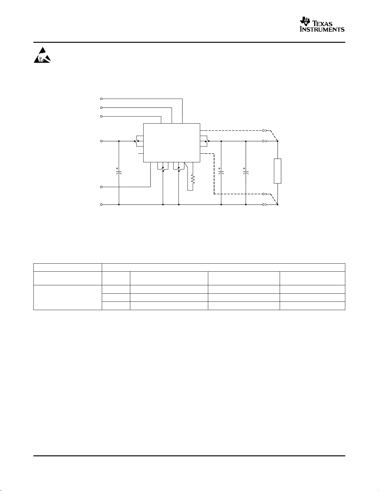
STANDARD APPLICATION
Track
Margin Up
Margin Down
C
I
m
560 F
(Required)
2
4
6
8
V
Inhibit
I
19 20
MarginUpMargin
V
I
PTH12040W
UVLO Prog
Inhibit
GND
7
1
18
Track
Down
+Sense
-Sense
GND
3510 13 16
V Adj
O
V
O
17
R
1%
0.05 W
SET
11
9
12
15
14
C1
O
330 F
m
(Required)
+Sense
V
O
C2
O
m
330 F
(Required)
-Sense
L
O
A
D
GND
A. R
= Required to set the output voltage higher than the minimum value (see the elcetrical characheristics for
SET
values.)
B. CI= Required 560-µF electrolytic capacitor. 1000 µF recommended.
C. CO= Required 660-µF (or 680 µF) electrolytic capacitor.
ORDERING INFORMATION
PTH12040W PACKAGE OPTIONS (PTH12040Wxx)
VOLTAGE CODE DESCRIPTION Pb – free and RoHS PACKAGE REF
AH Horizontal T/H Yes EVF
0.8 V – 5.5 V (Adjust) AS Standard SMD
AZ Lead (Pb) – free SMD
(3)
(4)
(1) Add T to end of part number for tape and reel on SMD packages only.
(2) Reference the applicable package reference drawing for the dimensions and PC board layout.
(3) Standardoption specifies 63/37, Sn/Pb pin solder material.
(4) Pb – free option specifies Sn/Ag pin solder material.
Compatible
No EVG
Yes EVG
GND
(1)
(2)
2
Page 3
PTH12040W
www.ti.com
SLTS237A–DECEMBER 2004 – REVISED OCTOBER 2005
ABSOLUTE MAXIMUM RATINGS
over operating free-air temperature range (unless otherwise noted)
UNIT
Signal input voltages Track control (pin 18) –0.3 V to VI+0.3V
T
T
T
T
(1) During soldering of package version, do not elevate peak temperature of the module, pins or internal components above the stated
Operating temperature range over VIrange –40°Cto85°C
A
Wave solder Surface temperature of module body or pins (5 PTH12040WAH 260°C
wave
temperature seconds)
Solder reflow
reflow
temperature
Storage temperature –40°C to 125°C
stg
Surface temperature of module body or pins
PTH12040WAS 235°C
PTH12040WAZ 260°C
Mechanical shock Per Mil-STD-883D, Method 2002.3, 1 msec, 1/2 Sine, mounted 500 G
Mechanical vibration Mil-STD-883D, Method 2007.2, 20–2000 Hz 15 G
Weight 17 grams
Flammability Meets UL94V-O
maximum.
(1)
(1)
(1)
ELECTRICAL CHARACTERISTICS
TA=25°C, VI=12V,VO= 3.3 V, CI= 1000 µF, CO= 660 µF, and IO=IOmax (unless otherwise stated)
PARAMETER TEST CONDITIONS MIN TYP MAX UNIT
I
O
V
I
tol Set-point voltage tolerance ±2
V
O
∆Reg
∆Reg
∆Reg
∆Reg
∆Reg
η Efficiency I
V
R
trip Overcurrent threshold Reset, followed by auto-recovery 95 A
I
O
t
rr
∆V
tr
adj Margin up/down adjust With Margin up/down control ±5%
V
O
margin Margin input current Pin to GND –8
I
IL
I
track Track input current (pin 18) Pin to GND –0.10
IL
dV
track
Output current 60°C, 200 LFM airflow 0 50
Input voltage range Over IOrange 8
Temperature variation –40°C<TA<85°C ±0.5 %V
temp
Line regulation Over VIrange ±5mV
line
Load regulation Over IOrange ±5mV
load
Total output variation Includes set-point, line, load, –40°C ≤ TA≤ 85°C ±3
tot
Output adjust range 0.8 5.5
adj
= 205 Ω,VO= 5.0 V 96%
R
SET
=1.5kΩ,VO= 3.3 V 95%
R
SET
=3.01kΩ,VO= 2.5 V 93%
R
SET
=4.99kΩ,VO= 2.0 V 92%
R
SET
=35A R
O
=6.34kΩ,VO= 1.8 V 91%
SET
=9.76kΩ,VO= 1.5 V 90%
R
SET
= 18.2 kΩ,VO= 1.2 V 88%
R
SET
= 38.3 kΩ,VO= 1.0 V 86%
R
SET
= open circuit, VO= 0.8 V 82%
R
SET
(2)
VOripple (pk-pk) 20 MHz bandwidth All voltages 15 mVpp
Transient response 1 A/µs load step, 50 to 100% I
max, CO= 660 µF
O
Recovery time 70 µSec
VOover/undershoot 150 mV
(4)
/dt Track slew rate capability |V
TRACK–VO
| ≤ 50 mV and V
TRACK<VO
(nom) 1 V/ms
(1)
14 V
(2)
(2)
(3)
(5)
%V
%V
mA
A
O
O
O
V
µA
(1) See SOA curves or consult factory for appropriate derating.
(2) The set-point voltage tolerance is affected by the tolerance of R
with 100 ppm/°C or better temperature stability.
. The stated limit is unconditionally met if R
SET
has a tolerance of 1%
SET
(3) When the set-point voltage is adjusted higher than 3.6 V, a 10-V minimum input voltage is recommended.
(4) A small, low-leakage (<100 nA) MOSFET is recommended to control this pin. The open-circuit voltage is less than 1 Vdc.
(5) This control pin has an internal pull-up to 6.7 V. If left open-circuit, the module operates when input power is applied. A small, low
leakage (<100 nA) MOSFET or open-drain/collector voltage supervisor IC is recommended for control. See the Application Information
section for further guidance.
3
Page 4
www.ti.com
PTH12040W
SLTS237A–DECEMBER 2004 – REVISED OCTOBER 2005
ELECTRICAL CHARACTERISTICS (continued)
TA=25°C, VI=12V,VO= 3.3 V, CI= 1000 µF, CO= 660 µF, and IO=IOmax (unless otherwise stated)
PARAMETER TEST CONDITIONS MIN TYP MAX UNIT
UVLO Undervoltage lockout Pin 8 open On-threshold 7.5
Hysterisis 1
Inhibit control (pin 7) Referenced to GND
V
IH
V
IL
inhibit Input low current Pin to GND 0.5 mA
I
IL
inh Input standby current Inhibit (pin 7) to GND 35 mA
I
I
f
s
C
I
C
O
Input high voltage 2.5 Open
Input low voltage –0.2 0.5
Switching frequency Over VIand IOranges 0.9 1.05 1.2 MHz
External input capacitance 560
External output capacitance Ceramic 400
Capacitance value µF
Nonceramic 660
Equivalent series resistance (non-ceramic) 2
MTBF Reliability Per Bellcore TR-332 50% stress, T
=40°C, ground benigh
A
(6) Default voltages may be adjusted using the UVLO Prog control input. See the Application Information section for further guidance.
(7) This control pin has an internal pull-up to 5 V nominal. If it is left open-circuit, the module operates when input power is applied. A small,
low-leakage (<100 nA) MOSFET is recommended for control. For further information, see the related application note.
(8) A minimum capacitance of 560-µF is required at the input for proper operation. For best results, 1000 µF is recommended. The
capacitance must be rated for a minimum of 300 mArms of ripple current.
(9) A minimum value of output capacitance is required for proper operation. Adding additional capacitance at the load further improves
transient response.
(10) This is the calculated maximum. The minimum ESR requirement often results in a lower value. See the Application Information section
for further guidance.
(11) This is the typcial ESR for all the electrolytic (nonceramic) output capacitance. Use 4 mΩ as the minimum when using max-ESR values
to calculate.
(6)
(6)
(8)
1000 µF
(9)
(11)
14000
2.5
(10)
V
(7)
V
mΩ
6
10
Hrs
4
Page 5
PTH12040W
www.ti.com
SLTS237A–DECEMBER 2004 – REVISED OCTOBER 2005
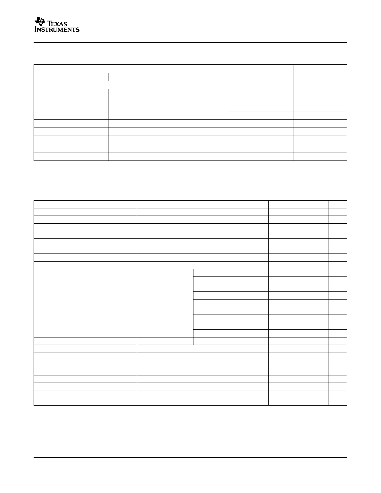
DEVICE INFORMATION
TERMINAL FUNCTIONS
TERMINAL
NAME NO.
GND
V
I
V
O
1, 3, 5, 10, 13, The common ground connection for the VIand VOpower connections. It is also the 0 Vdcreference for
16 the control inputs.
2, 4, 6 The positive input voltage power node to the module, which is referenced to common GND.
9, 12, 15 The regulated positive power output with respect to the GND node.
The Inhibit pin is an open-collector/drain negative logic input that is referenced to GND. Applying a
Inhibit
(1)
7
lowlevel ground signal to this input disables the module’s output and turns off the output voltage. When
the Inhibit control is active, the input current drawn by the regulator is significantly reduced. If the Inhibit
pin is left open-circuit, the module produces an output whenever a valid input source is applied.
A 1%, 0.05-W resistor must be connected between this pin and GND to set the output voltage higher
than the minimum value. The set-point range for the output voltage is from 0.8 V to 5.5 V. The resistor
VOAdjust 17 required for a given output voltage may be calculated from the following formula. If left open circuit, the
module output defaults to its lowest output voltage value. For further information on the adjustment
and/or trimming of the output voltage, see the related Application Information section.
R
set
+ 10 kW
0.8 V
VO* 0.8 V
* 1.696 kW
The specification table gives the preferred resistor values for a number of standard output voltages.
The sense inputs allow the regulation circuit to compensate for voltage drop between the module and
+Sense 11 the load. For optimal voltage accuracy, +Sense should be connected to VO. If it is left open, a low-value
internal resistor ensures that the output remains in regulation.
–Sense 14
For optimal voltage accuracy, –Sense should be connected to the ground return at the load. If it is left
open, a low-value internal resistor ensures that the output remains in regulation.
Connecting a resistor from this pin to signal ground allows the on threshold of the input undervoltage
UVLO Prog 8
lockout (UVLO) to be adjusted higher than the default value. The hysterisis can also be independenly
reduced by connecting a second resistor from this pin to VI. For further information, see the Application
Information section.
This is an analog control input that allows the output voltage to follow another voltage during power up
and power down sequences. The pin is active from 0 V, up to the nominal set-point voltage. Within this
Track 18
range, the module output follows the voltage at the Track pin on a volt-for-volt basis. When the control
voltage is raised above this range, the module regulates at its nominal output voltage. If unused, this
input should be connected to VIfor a faster power up. For further information, see the Application
Information section.
Margin
(1)
Down
Margin Up
20 requires an open-collector (open-drain) interface. It is not TTL compatible. A lower percent change can
(1)
19 collector (open-drain) interface. It is not TTL compatible. The percent change can be reduced with a
When this input is asserted to GND, the output voltage is decreased by 5% from the nominal. The input
be accommodated with a series resistor. For further information, see the Application Information section.
When this input is asserted to GND, the output voltage is increased by 5%. The input requires an open
series resistor. For further information, see the Application Information section.
(1) Denotes negative logic: Open = Normal operation / Ground = Function active
DESCRIPTION
17
18
19
20
16
15
13
14
PTHXX040W
1
2
3
12
(Top View)
4
5
891011
7
6
5
Page 6
www.ti.com
2
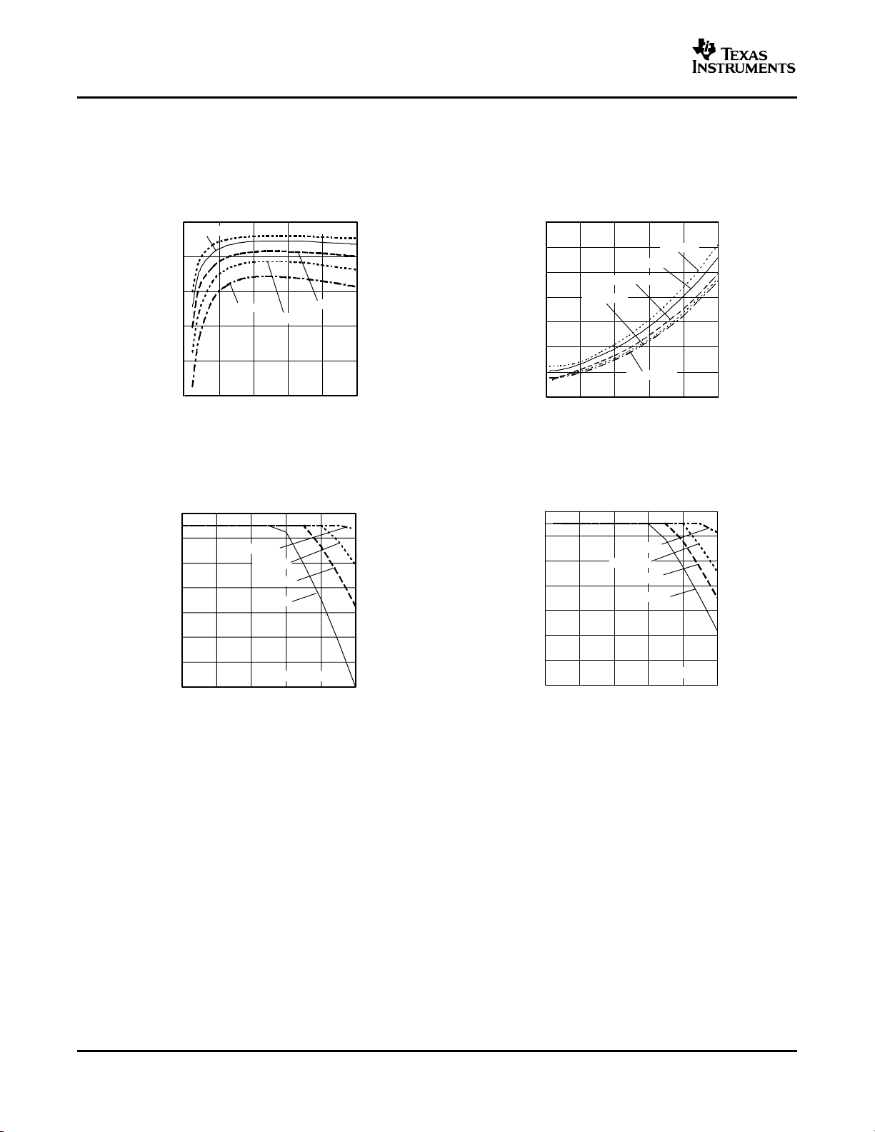
4
6
8
10
12
14
I
O
- Output Current - A
VO=5V
VO= 3.3 V
V
O
= 1.8 V
VO= 1.2 V
VO= 0.8 V
01020304050
0
- Power Dissipation - W
P
D
PTH12040W
SLTS237A–DECEMBER 2004 – REVISED OCTOBER 2005
TYPICAL CHARACTERISTICS
Characteristic Data (VI=12V)
EFFICIENCY POWER DISSIPATION
vs vs
LOAD CURRENT LOAD CURRENT
100
VO= 3.3 V
90
VO=5V
(1)(2)
80
VO= 0.8 V
70
Efficiency - %
60
50
0 1020 3040 50
I - Output Current - A
O
VO= 1.8 V
VO= 1.2 V
Figure 1. Figure 2.
TEMPERATURE DERATING TEMPERATURE DERATING
vs vs
OUTPUT CURRENT OUTPUT CURRENT
90
80
o
70
60
50
40
- Ambient Temperature - C
A
T
30
20
01020304050
400 LFM
200 LFM
100 LFM
Nat Conv
VO= 3.3 V
IO- Output Current - A
90
80
o
70
60
50
40
- Ambient Temperature - C
A
T
30
20
01020304050
400 LFM
200 LFM
100 LFM
Nat Conv
I
- Output Current - A
O
VO= 1.2 V
Figure 3. Figure 4.
(1) The electrical characteristic data has been developed from actual products tested at 25°C. This data is considered typical for the
converter. Applies to Figure 1 and Figure 2.
(2) The temperature derating curves represent the conditions at which internal components are at or below the manufacturer's maximum
operating temperatures. Derating limits apply to modules soldered directly to a 4-mm x 4-mm, double-sided PCB with 1-oz. copper. For
surface mount packages (AS and AZ suffix), multiple vias (plated through holes) are required to add thermal paths around the power
pins. Please refer to the mechanical specification for more information. Applies to Figure 3 and Figure 6.
6
Page 7
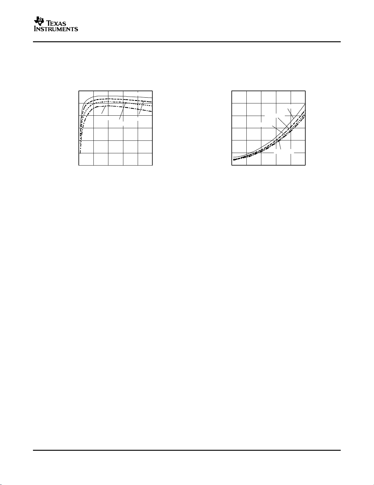
0
2
4
6
8
10
12
VO= 3.3 V
VO= 1.8 V
VO= 1.2 V
VO= 0.8 V
01020304050
P Power Dissipation - W
D
-
I - Output Current - A
O
PTH12040W
www.ti.com
TYPICAL CHARACTERISTICS
Characteristic Data (VI=8V)
(4)(5)
(continued)
(3)
SLTS237A–DECEMBER 2004 – REVISED OCTOBER 2005
EFFICIENCY POWER DISSIPATION
vs vs
LOAD CURRENT LOAD CURRENT
100
90
80
70
Efficiency - %
60
50
40
VO= 0.8 V
01020304050
I - Output Current - A
O
VO= 3.3 V
VO= 1.8 V
VO= 1.2 V
Figure 5. Figure 6.
(3) The electrical characteristic data has been developed from actual products tested at 25°C. This data is considered typical for the
converter. Applies to Figure 5 , and Figure 6.
7
Page 8

www.ti.com
PTH12040W
SLTS237A–DECEMBER 2004 – REVISED OCTOBER 2005
APPLICATION INFORMATION
Capacitor Recommendations for the PTH12040W Power Module
The PTH12040W is a state-of-the-art multi-phase power converter topology that uses three parallel switching and
filter inductor paths between the common input and output filter capacitors. The three paths share the load
current, operate at the same frequency, and are evenly displaced in phase.
With multiple switching paths the transient output current capability is significantly increased. This reduces the
amount of external output capacitance required to support a load transient. As a further benefit, the ripple
current, as seen by the input and output capacitors, is reduced in magnitude and effectively tripled in frequency.
Input Capacitor
The improved transient response of a multi-phase converter places a bigger burden on the transient capability of
the input source. The size and value of the input capacitor is therefore determined by this converter’s transient
performance capability. The minimum amount of input capacitance required is 560 µF, with an RMS ripple
current rating of 300 mA. This minimum value assumes that the converter is supplied with a responsive, low
inductance input source. This source should have ample capacitive decoupling, and be distributed to the
converter via PCB power and ground planes. For high-performance applications, or wherever the transient
performance of the input source is limited, 1000 µF of input capacitance is recommended.
Ripple current, less than 100 mΩ of equivalent series resistance (ESR), and temperature are the main
considerations when selecting input capacitors. The ripple current reflected from the input of the PTH12040W
module is moderate to low. Therefore any good quality, computer-grade electrolytic capacitor, of either value
suggested, has an adequate ripple current rating.
Regular tantalum capacitors are not recommended for the input bus. These capacitors require a recommended
minimum voltage rating of 2 × (maximum dc voltage + ac ripple). This is standard practice to ensure reliability. No
tantalum capacitors were found with a sufficient voltage rating to meet this requirement. When the operating
temperature is below 0°C, the ESR of aluminum electrolytic capacitors increases. For these applications,
Os-Con, polyaluminum, and polymer-tantalum types should be considered. Adding one or two ceramic capacitors
to the input reduces high-frequency reflected ripple current.
Output Capacitors
The PTH12040W requires a minimum output capacitance of 660 µF (or 2 × 330 µF), with an ESR of 15 mΩ to
40 mΩ. This is necessary for the stable operation of the regulator. Additional capacitance can be added to
improve the module's performance to load transients. High quality computer-grade electrolytic capacitors are
recommended. Aluminum electrolytic capacitors provide adequate decoupling over the frequency range, 2 kHz to
150 kHz, and are suitable when ambient temperatures are above 0°C. For operation below 0°C, tantalum,
ceramic, or Os-Con type capacitors are necessary.
When using a combination of one or more nonceramic capacitors, the calculated equivalent ESR should be no
lower than 2 mΩ (4 mΩ when calculating using the manufacturer’s maximum ESR values). A list of preferred
low-ESR type capacitors are identified in Table 1.
Ceramic Capacitors
Above 150 kHz the performance of aluminum electrolytic capacitors is less effective. Multilayer ceramic
capacitors have very low ESR and a resonant frequency higher than the bandwidth of the regulator. They can be
used to reduce the reflected ripple current at the input as well as improve the transient response of the output.
When used on the output their combined ESR is not critical as long as the total value of ceramic capacitors, with
values between 10 µF and 100 µF, does not exceed 400 µF. Also, to prevent the formation of local resonances,
do not place more than five identical ceramic capacitors in parallel with values of 10 µF or greater.
8
Page 9

PTH12040W
www.ti.com
SLTS237A–DECEMBER 2004 – REVISED OCTOBER 2005
APPLICATION INFORMATION (continued)
Tantalum Capacitors
Tantalum type capacitors are only used on the output bus, and are recommended for applications where the
ambient operating temperature is less than 0°C. The AVX TPS, Sprague 593D/594/595 and Kemet T495/T510
capacitor series are suggested over many other tantalum types due to their higher rated surge, power
dissipation, and ripple current capability. As a caution, many general purpose tantalum capacitors have higher
ESR, reduced power dissipation, and lower ripple current capability. These capacitors are also less reliable due
to their reduced power dissipation and surge current ratings. Tantalum capacitors that have no stated ESR or
surge current rating are not recommended for power applications.
When specifying Os-con and polymer-tantalum capacitors for the output, the minimum ESR limit is encountered
well before the maximum capacitance value is reached.
Capacitor Table
Table 1 identifies the characteristics of capacitors from a number of vendors with acceptable ESR and ripple
current (rms) ratings. The recommended number of capacitors required at both the input and output buses is
identified for each capacitor type.
Note: This is not an extensive capacitor list. Capacitors from other vendors are available with comparable
specifications. Those listed are for guidance. The RMS ripple current rating and ESR (at 100 kHz) are critical
parameters necessary to insure both optimum regulator performance and long capacitor life.
Designing for Very Fast Load Transients
The transient response of the dc/dc converter has been characterized using a load transient with a di/dt of
1 A/µs. The typical voltage deviation for this load transient is given in the data sheet specification table using the
mnimum required value of output capacitance. As the di/dt of a transient is increased, the response of a
converter’s regulation circuit ultimately depends on its output capacitor decoupling network. This is an inherent
limitation with any dc/dc converter once the speed of the transient exceeds its bandwidth capability. If the target
application specifies a higher di/dt or lower voltage deviation, the requirement can only be met with additional
output capacitor decoupling. In these cases special attention must be paid to the type, value and ESR of the
capacitors selected.
9
Page 10

www.ti.com
PTH12040W
SLTS237A–DECEMBER 2004 – REVISED OCTOBER 2005
APPLICATION INFORMATION (continued)
Table 1. Input/Output Capacitors
Capacitor Characteristics Quantity
Capacitor Vendor,
Type Series (Style)
Working Value Max. ESR Physical Input Output
Voltage (µF) at 100 kHz Size (mm) Bus Bus
Panasonic 25 V 1000 0.043 Ω >1690 mA 16 × 15 1 1 EEUFC1E102S
FC (Radial) 25 V 560 0.065 Ω 1205 mA 12,5 × 15 1 2 EEUFC1E561S
16 V 680 0.080 Ω >850 mA 10 × 10,2 1 1 EEVFK1C681P
FK (SMD) 35 V 1000 0.060 Ω 1100 mA 12,5 × 13,5 1 1 EEVFK1V102Q
United Chemi-Con 16 V 470 0.090 Ω 670 mA 10 × 10 2 2 MVZ25VC471MJ10TP
MVZ(SMD) 16 V 470 0.090 Ω 760 mA 10 × 12,5 2 2 LXZ16VB471M10X12LL
LXZ, Aluminum (Radial) 25 V 680 0.068 Ω 1050 mA 10 × 16 1 1 LXZ16VB681M10X16LL
PS, Poly-Aluminum(Radial) 16 V 330 0.014 Ω 5060 mA 10 × 12,5 2 ≤4 16PS330MJ12
PXA, Poly-Aluminum (SMD) 16 V 330 0.014 Ω 5050 mA 10 × 12,2 2 ≤4 PXA16VC331MJ12TP
Nichicon, Aluminum 25 V 560 0.060 Ω 1060 mA 12,5 × 15 1 2 UPM1E561MHH6
HD (Radial) 25 V 680 0.038 Ω 1430 mA 10 × 16 1 1 UHD1C681MHR
PM (Radial) 35 V 560 0.048 Ω 1360 mA 16 × 15 1 2 UPM1V561MHH6
Panasonic, Poly-Aluminum:
SP-Cap 6.3 V 180 0.005 Ω 4100 mA 7,3 × 5,7 N/R
Sanyo 10 V
TPE, Poscap (SMD) 16 V 330 0.025 Ω 3000 mA 7,3 × 5,7 N/R
SP, Os-Con (Radial) 16 V 470 0.010Ω >6000 mA 10 × 13 ≤ 4 16SEPC470M
SVP, Os-Con (SMD) 330 0.016 Ω 4700 mA 11 × 12 3
AVX, Tantalum, Series III 10 V 470 0.045 Ω >1723 mA 7,3 ×5,7 ×4,1 N/R
TPS (SMD) 10 V 330 0.045 Ω 1723 mA N/R
Kemet, Poly-Tantalum 10 V 330 0.040 Ω 1800 mA 4,3 ×7,3 ×4,0 N/R
T520 (SMD) 10 V 330 0.015 Ω >3800 mA N/R
T530 (SMD) ( Poly-Tantalum ) 6.3 V 470 0.012 Ω 4200 mA N/R
T530 (SMD) ( Poly-Tantalum ) 4 V 680 0.005 Ω >5000 mA 7,3 ×4,3 ×4.0 N/R
Vishay-Sprague
595D, Tantalum (SMD) 10 V 470 0.100 Ω 1440 mA 7,2 × 6× 4,1 N/R
94SA, Os-con (Radial) 16 V 1000 0.015 Ω 9740 mA 16 × 25 1 ≤4 94SA108X0016HBP
Kemet, Ceramic X5R (SMD) 16 V 10 0.002 Ω –1
6.3 V 47 0.002 Ω N/R
Murata, Ceramic X5R (SMD) 6.3 V 100 – – N/R
6.3 V 47 N/R
16 V 47 3225 1
16 V 22 1
16 V 10 1
TDK, Ceramic X5R (SMD) 6.3 V 100 – – N/R
6.3 V 47 N/R
16 V 22 1
16 V 10 1
(1) Capacitor Supplier Verification
Please verify availability of capacitors identified in this table. Capacitor suppliers may recommend alternative part numbers because of
limited availability or obsolete products. In some instances, the capacitor product life cycle may be in decline and have short-term
consideration for obsolescence.
RoHS, Lead-free and Material Details
Please consult capacitor suppliers regarding material composition, RoHS status, lead-free status, and manufacturing process
requirements. Component designators or part number deviations can occur when material composition or soldering requirements are
updated.
(2) N/R – Not recommended. The voltage rating does not meet the minimum operating limits.
(3) Total capacitance of 540 µF is acceptable based on the combined ripple current rating.
(4) The voltage rating of this capacitor only allows it to be used for utput voltages that are equal to or less than 5.1 V.
(5) Small ceramic capacitors may be used to complement electrolytic types at the input to further reduce high-frequency ripple current.
Max Ripple
Current at Vendor Part No.
85°C (Irms)
3225
3225
(1)
2
(2)
≤5 EEFSE09J181R (VO≤ 5.1 V)
(2)
≤5 10TPE330M
(3)
≤4 16SVP330M
(2)
(4)
≤5
(2)
(2)
(2)
(2)
(2)
(2)2(4)
(5)
(2)
(2)
(2)
(5)
(5)
(5)
(2)
(2)
(5)
(5)
TPSE477M010R0045 (VO≤ 5.1 V)
(4)
≤5
TPSE337M010R0045 (VO≤ 5.1 V)
2 T520X337M010AS
≤4 T530X337M010AS
(4)
≤3
T530X477M006AS (VO≤ 5.1 V)
≤2 T530X687M004ASE005 (VO≤ 3.2
(4)
V)
≤3
595D477X0010R2T (VO≤ 5.1 V )
≤8 C1210C106M4PAC
≤8 C1210C476K9PAC
≤4 GRM32ER60J107M
≤ 8 GRM32ER60J476M
≤ 8 GRM32ER61C476K
≤ 8 GRM32ER61C226K
≤ 8 GRM32DR61C106K
≤4 C3225X5R0J107MT
≤ 8 C3225X5R0J476MT
≤ 8 C3225X5R1C226MT
≤ 8 C3225X5R1C106MT
10
Page 11

PTH12040W
www.ti.com
SLTS237A–DECEMBER 2004 – REVISED OCTOBER 2005
APPLICATION INFORMATION (continued)
Adjusting the Output Voltage of the PTH12040W Wide-Output Adjust Power Module
The VOAdjust control (pin 17) sets the output voltage of the PTH12040W product. The adjustment range is from
0.8 V to 5.5 V. The adjustment method requires the addition of a single external resistor, RSET, that must be
connected directly between the VOAdjust and GND pins 1. Table 2 gives the preferred value of the external
resistor for a number of standard voltages, along with the actual output voltage that this resistance value
provides. Figure 7 shows the placement of the required resistor.
For other output voltages, the value of the required resistor can either be calculated, or simply selected from the
range of values given in Table 3. The following formula can be used to calculate the adjust resistor value.
R
set
+ 10 kW
0.8 V
VO* 0.8 V
* 1.696 kW
Table 2. Standard Values of R
VO(Required) R
5V 2.5Ω 5.008 V
3.3 V 1.5 kΩ 3.303 V
2.5 V 3.01 kΩ 2.5 V
2 V 4.99 kΩ 1.997 V
1.8 V 6.34 kΩ 1.796 V
1.5 V 9.76 kΩ 1.498 V
1.2 V 18.2 kΩ 1.202 V
1 V 38.3 kΩ 1V
0.8 V Open 0.8 V
Voltages
SET
for Common Output
SET
PTH12040W
VO(Actual)
(1)
+Sense
V
O
C
O
m
m
330 F
-Sense
GND
PTH12040W
GND GND
3510 13 16
1
+Sense
V
-Sense
V Adj
O
O
17
R
1%
0.05 W
SET
11
9
12
15
14
C
O
330 F
(1) A 0.05-W rated resistor may be used. The tolerance should be 1%, and the temperature stability, 100 ppm/°C(or
better). Place the resistor as close to the regulator as possible. Connect the resistor directly between pin 17 and
nearest GND pin (pin 16) using dedicated PCB traces.
(2) Never connect capacitors from VoAdjust to either GND or VO. Any capacitance added to the VoAdjust pin affects the
stability of the regulator.
Figure 7. VoAdjust Resistor Placement
11
Page 12

www.ti.com
PTH12040W
SLTS237A–DECEMBER 2004 – REVISED OCTOBER 2005
Table 3. Output Voltage Set-Point Resistor Values
V
O
0.8 Open 1.6 8.3 kΩ 3.05 1.86 kΩ
0.825 318 kΩ 1.65 7.72 kΩ 3.1 1.78 kΩ
0.85 158 kΩ 1.7 7.19 kΩ 3.15 1.71 kΩ
0.875 105 kΩ 1.75 6.73 kΩ 3.2 1.64 kΩ
0.9 78.31 kΩ 1.8 6.3 kΩ 3.25 1.57 kΩ
0.925 62.3 kΩ 1.85 5.92 kΩ 3.3 1.5 kΩ
0.95 51.6 kΩ 1.9 5.58 kΩ 3.35 1.44 kΩ
0.975 44 kΩ 1.95 5.26 kΩ 3.4 1.38 kΩ
1 38.3 kΩ 24.97kΩ 3.5 1.27 kΩ
1.025 33.9 kΩ 2.05 4.7 kΩ 3.6 1.16 kΩ
1.05 30.3 kΩ 2.1 4.46 kΩ 3.7 1.06 kΩ
1.075 27.4 kΩ 2.15 4.23 kΩ 3.8 971 Ω
1.1 25 kΩ 2.2 4.02 kΩ 3.9 885 Ω
1.125 22.9 kΩ 2.25 3.82 kΩ 4 804 Ω
1.15 21.2 kΩ 2.3 3.64 kΩ 4.1 728 Ω
1.175 19.6 kΩ 2.35 3.47 kΩ 4.2 657 Ω
1.2 18.3 kΩ 2.4 3.3 kΩ 4.3 590 Ω
1.225 17.1 kΩ 2.45 3.15 kΩ 4.4 526 Ω
1.25 16.1 kΩ 2.5 3.01 kΩ 4.5 466 Ω
1.275 15.1 kΩ 2.55 2.88 kΩ 4.6 409 Ω
1.3 14.3 kΩ 2.6 2.75 kΩ 4.7 355 Ω
1.325 13.5 kΩ 2.65 2.63 kΩ 4.8 304 Ω
1.35 12.8 kΩ 2.7 2.51 kΩ 4.9 255 Ω
1.375 12.2 kΩ 2.75 2.41 kΩ 5 209 Ω
1.4 11.6 kΩ 2.8 2.3 kΩ 5.1 164 Ω
1.425 11.1 kΩ 2.85 2.21 kΩ 5.2 122 Ω
1.45 10.6 kΩ 2.9 2.11 kΩ 5.3 82 Ω
1.475 10.2 kΩ 2.95 2.02 kΩ 5.4 43 Ω
1.5 9.73 kΩ 31.94kΩ 5.5 0 Ω
1.55 8.97 kΩ
R
SET
V
O
R
SET
V
O
R
SET
Adjusting the Undervoltage Lockout (UVLO) of the PTH12040W Power Modules
The PTH12040W power modules incorporate an input undervoltage lockout (UVLO). The UVLO feature prevents
the operation of the module until there is sufficient input voltage to produce a valid output voltage. This enables
the module to provide a clean, monotonic powerup for the load circuit, and also limits the magnitude of current
drawn from the regulator’s input source during the power-up sequence.
The UVLO characteristic is defined by the on-threshold (V
threshold, the Inhibit control is overriden, and the module does not produce an output. The hysterisis voltage is
the difference between the on and off threshold voltages. It ensures a clean power-up, even when the input
voltage is rising slowly. The hysterisis prevents start-up oscillations, which can occur if the input voltage droops
slightly when the module begins drawing current from the input source.
12
) and hysterisis (V
THD
) voltages. Below the on
HYS
Page 13

PTH12040W
www.ti.com
SLTS237A–DECEMBER 2004 – REVISED OCTOBER 2005
UVLO Adjustment
The UVLO feature of the PTH12040W module allows for limited adjustment of both the on threshold and
hysterisis voltages. The adjustment is made via the UVLO Prog control pin. When the UVLO Prog pin is left open
circuit, the on threshold and hysterisis voltages are internally set to their default values. The on threshold has a
nominal voltage of 7.5 V, and the hysterisis 1 V. This ensures that the module produces a regulated output when
the minimum input voltage is applied (see specifications). The combination correlates to an off threshold of
approximately 6.5 V. The adjustments are limited. The on threshold can only be adjusted higher, and the
hysterisis voltage can only be reduced in magnitude.
The on threshold might need to be raised if the module is powered from a tightly regulated 12-V bus. This would
prevent it from operating if the input bus failed to completely rise to its specified regulation voltage. The hysterisis
should not be changed unless absolutely necessary. A generous amount of hysterisis ensures that the module
exhibits a clean startup. Therefore, adjustment of the hysterisis should only be considered if there is a system
requirement to specifically set the off threshold voltage (in addition to the on threshold). Depending on the load
regulation of the input source, the hysterisis should not be adjusted below 0.5 V without careful consideration.
Adjustment Method
The resistors, R
R
connects between the UVLO Prog control pin and GND, and R
THD
and VI.R
alone is used to adjust the on-threshold voltage higher. However, to adjust the hystersis to a lower
THD
value requires both the R
The recommended adjustment method requires that any change to the hysterisis be determined first. If the
hysterisis is changed, then a value for R
required to the value of V
location. R
HYS
THD
and R
(see Figure 8), provide the adjustment of the on-threshold and hysterisis voltages.
HYS
and R
HYS
. If there is no change to V
THD
resistors to be placed in the circuit.
THD
must also be calculated. This is irrespective of whether a change is
THD
, then a resistor should not be placed in the R
HYS
is connected between the UVLO Prog
HYS
should then be assigned an infinite value for calculating the value of R
THD
.
HYS
V
GND
I
1000 Fm
R
HYS
C
I
R
THD
2
4
V
PTH12040W
I
6
8
UVLO Prog
Inhibit GND
7
135
Figure 8. UVLO Program Resistor Placement
Hysterisis Adjust
The hysterisis voltage, V
is the difference between the on and off threshold values. The default value is 1 V
HYS,
and it can only be adjusted to a lower value.
Caution should be used when changing the hysterisis voltage to a lower value, as it could induce
start-up oscillations.
Any change in the hysterisis voltage requires both R
not have the desired effect. The value for R
R
must then be used to determine a value for R
HYS
must first be calculated using Equation 2. The value identified for
HYS
and R
HYS
, using Equation 3.
THD
THD
resistors be in place. Adding R
alone does
HYS
13
Page 14

www.ti.com
PTH12040W
SLTS237A–DECEMBER 2004 – REVISED OCTOBER 2005
R
HYS
+
0.365 ǒ1 * V
Threshold Adjust
Equation 3 determines the value of R
may only be adjusted to a higher value. If the hysterisis value has been adjusted, then a value for R
be calculated. (This is irrespective of whether V
hystersis voltage, the term 1/R
26.1 H
R
THD
+
39.2ƪ(1ńR
Calculated Values
Table 4 shows a matrix of standard resistor values for R
(V
) and hysterisis (V
THD
adjusted. In this case select only a value for R
The hysterisis should only be adjusted if there is a specific requirement to independently adjust the off-threshold,
separately from the on-threshold voltage. In this case, a value for both R
Table 4. This is irrespective of whether the on-threshold voltage is being adjusted.
HYS
HYS
HYS
kW
Ǔ
required to adjust V
THD
is being adjusted.) If there has been no adjustment for the
THD
in Equation 3, may be assigned the value, 0.
to a new value. The default value is 7.5 V, and it
THD
must also
THD
39.2 kW
ǒ
) 0.014
HYS
) voltages. For most applications, only the on-threshold voltage should need to be
HYS
Ǔ
V
ń2.5 * 1Ǔ* 0.0027ƫ*1
THD
and R
HYS
from far right-hand column.
THD
, for different options of the on-threshold
THD
HYS
and R
must be selected from
THD
(2)
(3)
Table 4. Calculated Values of R
V
HYS
V
THD
8V 30.1 kΩ 43.2 kΩ 63.4 kΩ 97.6 kΩ 169 kΩ 402 kΩ
8.5 V 25.5 kΩ 36.5 kΩ 51.1 kΩ 73.2 kΩ 110 kΩ 187 kΩ
9V 23.2 kΩ 30.9 kΩ 42.2 kΩ 57.6 kΩ 82.5 kΩ 124 kΩ
9.5 V 20 kΩ 27.4 kΩ 36.5 kΩ 48.7 kΩ 64.9 kΩ 90.9 kΩ
10 V R
10.5 V 16.2 kΩ 21.5 kΩ 28 kΩ 36.5 kΩ 46.4 kΩ 60.4 kΩ
11 V 15 kΩ 19.6 kΩ 25.5 kΩ 32.4 kΩ 41.2 kΩ 52.3 kΩ
11.5 V 14 kΩ 18.2 kΩ 23.2 kΩ 28 kΩ 36.5 kΩ 45.3 kΩ
12 V 12.7 kΩ 16.5 kΩ 21 kΩ 26.1 kΩ 32.4 kΩ 40.2 kΩ
R
HYS
THD
0.5 V 0.6 V 0.7 V 0.8 V 0.9 V
71.5 kΩ 107 kΩ 165 kΩ 287 kΩ 649 kΩ N/A
18.2 kΩ 24.3 kΩ 31.6 kΩ 41.2 kΩ 54.9 kΩ 73.2 kΩ
HYS
and R
V
THD
, for Various Values of V
THD
HYS
(default)
and
1V
Features of the PTH Family of Non-Isolated Wide Output Adjust Power Modules
POLA™ Compatibility
The PTH/PTV family of nonisolated, wide-output adjustable power modules from Texas Instruments are
optimized for applications that require a flexible, high performance module that is small in size. Each of these
products are POLA™ compatible. POLA-compatible products are produced by a number of manufacturers, and
offer customers advanced, non-isolated modules with the same footprint and form factor. POLA parts are also
assured to be interoperable, thereby providing customers with second-source availability.
All POLA products include Auto-Track™. This feature was specifically designed to simplify the task of
sequencing the supply voltages in a power system. This and other features are described in the following
sections.
Soft-Start Power Up
The Auto-Track feature allows the power-up of multiple PTH modules to be directly controlled from the Track pin.
However in a stand-alone configuration, or when the Auto-Track feature is not being used, the Track pin should
be directly connected to the input voltage, VI(see Figure 9).
14
Page 15

PTH12040W
www.ti.com
8
9
Up Dn
12 V
++
GND
C
I
1000 F
m
V
I
PTH120 20W
GNDInhibit
1
3
Tr ack
7104
5
Sense
Adjust
R , 2 kHz
SET
1%
0.05 W
SLTS237A–DECEMBER 2004 – REVISED OCTOBER 2005
62
V
O
3.3 V
C
O
330 F
GND
m
Figure 9. Power-Up Application Circuit
When the Track pin is connected to the input voltage the Auto-Track function is permanently disengaged. This
allows the module to power up entirely under the control of its internal soft-start circuitry. When power up is
under soft-start control, the output voltage rises to the set-point at a quicker and more linear rate.
From the moment a valid input voltage is applied, the soft-start control introduces a short time delay (typically
8 ms–15 ms) before allowing the output voltage to rise.
V (5 V/Div)
I
V (1 V/Div)
O
I (5 A/Div)
I
HORIZTAL SCALE: 5 ms/Div
Figure 10. Power-Up Waveforms
The output then progressively rises to the module’s setpoint voltage. Figure 10 shows the soft-start power-up
characteristic of the 18-A output product (PTH12020W), operating from a 12-V input bus and configured for a
3.3-V output. The waveforms were measured with a 5-A resistive load and the Auto-Track feature disabled. The
initial rise in input current when the input voltage first starts to rise is the charge current drawn by the input
capacitors. Power-up is complete within 25 ms.
Overcurrent Protection
For protection against load faults, all modules incorporate output overcurrent protection. Applying a load that
exceeds the regulator’s overcurrent threshold causes the regulated output to shut down. Following shutdown, a
module periodically attempt to recover by initiating a soft-start power-up. This is described as a hiccup mode of
operation, whereby the module continues in a cycle of successive shutdown and power up until the load fault is
removed. During this period, the average current flowing into the fault is significantly reduced. Once the fault is
removed, the module automatically recovers and returns to normal operation.
15
Page 16

www.ti.com
PTH12040W
SLTS237A–DECEMBER 2004 – REVISED OCTOBER 2005
Overtemperature Protection (OTP)
The PTH12020, PTH12030, and PTH12040 products have overtemperature protection. These products have an
on-board temperature sensor that protects the module’s internal circuitry against excessively high temperatures.
A rise in the internal temperature may be the result of a drop in airflow, or a high ambient temperature. If the
internal temperature exceeds the OTP threshold, the module’s Inhibit control is internally pulled low. This turns
the output off. The output voltage drops as the external output capacitors are discharged by the load circuit. The
recovery is automatic, and begins with a soft-start power up. It occurs when the the sensed temperature
decreases by about 10°C below the trip point.
Note: The overtemperature protection is a last resort mechanism to prevent thermal stress to the regulator.
Operation at or close to the thermal shutdown temperature is not recommended and reduces the long-term
reliability of the module. Always operate the regulator within the specified safe operating area (SOA) limits for
the worst-case conditions of ambient temperature and airflow.
Output On/Off Inhibit
For applications requiring output voltage on/off control, each series of the PTH family incorporates an output
Inhibit control pin. The inhibit feature can be used wherever there is a requirement for the output voltage from the
regulator to be turned off.
The power modules function normally when the Inhibit pin is left open-circuit, providing a regulated output
whenever a valid source voltage is connected to VIwith respect to GND.
Figure 11 shows the typical application of the inhibit function. Note the discrete transistor (Q1). The Inhibit input
has its own internal pull-up to a potential of 5 V to 13.2 V (see footnotes to electrical characteristics table). The
input is not compatible with TTL logic devices. An open-collector (or open-drain) discrete transistor is
recommended for control.
V
Sense
O
V
I
560 F
1 = Inhibit
GND
10
PTH12060W
1
++
C
I
m
BSS138
3
Q1
9 8
7
5
4
R
SET
2k
1%
0.1 W
V
62
330 F
O
GND
L
O
A
D
C
O
m
Figure 11. Inhibit Control Circuit
Turning Q1 on applies a low voltage to the Inhibit control pin and disables the output of the module. If Q1 is then
turned off, the module executes a soft-start power-up sequence. A regulated output voltage is produced within 25
ms. Figure 12 shows the typical rise in both the output voltage and input current, following the turn-off of Q1. The
turn off of Q1 corresponds to the rise in the waveform, Q1 VDS. The waveforms were measured with a 5-A
constant current load.
16
Page 17

PTH12040W
www.ti.com
Q1 V (5 V/Div)
HORIZTAL SCALE: 10 ms/Div
SLTS237A–DECEMBER 2004 – REVISED OCTOBER 2005
DS
V (2 V/Div)
O
I (2 A/Div)
I
Figure 12. Power-Up from Inhibit Control
Remote Sense
Products with this feature incorporate an output voltage sense pin, VOSense. A remote sense improves the load
regulation performance of the module by allowing it to compensate for any IR voltage drop between its output
and the load. An IR drop is caused by the high output current flowing through the small amount of pin and trace
resistance.
To use this feature simply connect the VOSense pin to the VOnode, close to the load circuit. If a sense pin is left
open-circuit, an internal low-value resistor (15-Ω or less) connected between the pin and and the output node,
ensures the output remains in regulation.
With the sense pin connected, the difference between the voltage measured directly between the VOand GND
pins, and that measured from VOSense to GND, is the amount of IR drop being compensated by the regulator.
This should be limited to a maximum of 0.3 V.
Note: The remote sense feature is not designed to compensate for the forward drop of nonlinear or
frequency dependent components that may be placed in series with the converter output. Examples include
OR-ing diodes, filter inductors, ferrite beads, and fuses. When these components are enclosed by the remote
sense connection they are effectively placed inside the regulation control loop, which can adversely affect the
stability of the regulator.
Auto-Track™ Function
The Auto-Track function is unique to the PTH/PTV family, and is available with all POLA products. Auto-Track
was designed to simplify the amount of circuitry required to make the output voltage from each module power up
and power down in sequence. The sequencing of two or more supply voltages during power up is a common
requirement for complex mixed-signal applications that use dual-voltage VLSI ICs such as the TMS320™ DSP
family, microprocessors, and ASICs.
How Auto-Track™ Works
Auto-Track works by forcing the module output voltage to follow a voltage presented at the Track control pin
This control range is limited to between 0 V and the module set-point voltage. Once the Track-pin voltage is
raised above the set-point voltage, the module output remains at its set-point
(2)
. As an example, if the Track pin
(1)
of a 2.5-V regulator is at 1 V, the regulated output is 1 V. If the voltage at the Track pin rises to 3 V, the regulated
output does not go higher than 2.5 V.
When under Auto-Track control, the regulated output from the module follows the voltage at its Track pin on a
volt-for-volt basis. By connecting the Track pin of a number of these modules together, the output voltages follow
a common signal during power up and power down. The control signal can be an externally generated master
ramp waveform, or the output voltage from another power supply circuit
(3)
. For convenience, the Track input
incorporates an internal RC-charge circuit. This operates off the module input voltage to produce a suitable rising
waveform at power up.
17
.
Page 18

www.ti.com
PTH12040W
SLTS237A–DECEMBER 2004 – REVISED OCTOBER 2005
Typical Application
The basic implementation of Auto-Track allows for simultaneous voltage sequencing of a number of Auto-Track
compliant modules. Connecting the Track inputs of two or more modules forces their Track input to follow the
same collective RC-ramp waveform, and allows their power-up sequence to be coordinated from a common
Track control signal. This can be an open-collector (or open-drain) device, such as a power-up reset voltage
supervisor IC. See U3 in Figure 13.
To coordinate a power-up sequence, the Track control must first be pulled to ground potential. This should be
done at or before input power is applied to the modules. The ground signal should be maintained for at least
20 ms after input power has been applied. This brief period gives the modules time to complete their internal
soft-start initialization
that includes a built-in time delay, is an ideal component for automatically controlling the Track inputs at power
up.
Figure 13 shows how the TL7712A supply voltage supervisor IC (U3) can be used to coordinate the sequenced
power PTH12040W modules. The output of the TL7712A supervisor becomes active above an input voltage of
3.6 V, enabling it to assert a ground signal to the common Track control well before the input voltage has
reached the module's undervoltage lockout threshold. The ground signal is maintained until approximately 28 ms
after the input voltage has risen above U3's voltage threshold, which is 10.95 V. The 28-ms time period is
controlled by the capacitor C3. The value of 2.2 µF provides sufficient time delay for the modules to complete
their internal soft-start initialization. The output voltage of each module remains at zero until the Track control
voltage is allowed to rise. When U3 removes the ground signal, the Track control voltage automatically rises.
This causes the output voltage of each module to rise simultaneously with the other modules, until each reaches
its respective set-point voltage.
Figure 14 shows the output voltage waveforms from the circuit of Figure 13 after input voltage is applied to the
circuit. The waveforms, VO1 and VO2, represent the output voltages from the two power modules, U1 (3.3 V) and
U2 (1.8 V), respectively. V
power-up characteristic.
The same circuit also provides a power-down sequence. When the input voltage falls below U3's voltage
threshold, the ground signal is re-applied to the common Track control. This pulls the Track inputs to zero volts,
forcing the output of each module to follow, as shown in Figure 15. In order for a simultaneous power-down to
occur, the Track inputs must be pulled low before the input voltage has fallen below the modules' undervoltage
lockout. This is an important constraint. Once the modules recognize that a valid input voltage is no longer
present, their outputs can no longer follow the voltage applied at their Track input. During a power-down
sequence, the fall in the output voltage from the modules is limited by the maximum output capacitance and the
Auto-Track slew rate.
(4)
, enabling them to produce an output voltage. A low-cost supply voltage supervisor IC,
TRK,VO
1, and VO2 are shown rising together to produce the desired simultaneous
Notes on Use of Auto-Track™
1. The Track pin voltage must be allowed to rise above the module set-point voltage before the module
regulates at its adjusted set-point voltage.
2. The Auto-Track function tracks almost any voltage ramp during power up, and is compatible with ramp
speeds of up to 1 V/ms.
3. The absolute maximum voltage that may be applied to the Track pin is the input voltage VI.
4. The module cannot follow a voltage at its Track control input until it has completed its soft-start initialization.
This takes about 20 ms from the time that a valid voltage has been applied to its input. During this period, it
is recommended that the Track pin be held at ground potential.
5. The Auto-Track function is disabled by connecting the Track pin to the input voltage (VI). When Auto-Track is
disabled, the output voltage rises at a quicker and more linear rate after input power has been applied.
18
Page 19

PTH12040W
www.ti.com
V
= 12 V
I
U3
8
V
SENSE
RESIN
REF
CT
T
CC
TL7712A
GND
4
RESET
RESET
5
R
50 Ω
6
R
RST
10 kΩ2.2 µF
# R
C
REF
0.1 µF
= 100 Ω / N
TRK
7
2
1
3
C
N = Number of Track pins connected together
TRK
SLTS237A–DECEMBER 2004 – REVISED OCTOBER 2005
U1
2
4
V
I
6
8
UVLO Prog
Inhibit
+
C
I1
19 20 18
Margin
Margin
Down
Up
PTH12040W
GND GND
13510 13 16
7
Track
R
SET1
1.5 kΩ
+Sense
−Sense
VOAdj
17
11
9
12
V
O
15
14
Vo
= 3.3 V
1
+
C
O1
#
U2
2
4
V
I
6
8
UVLO Prog
Inhibit
+
C
I2
19 20 18
Margin
Margin
Down
Up
PTH12040W
GND GND
13510 13 16
7
Track
+Sense
−Sense
VOAdj
17
11
9
12
V
O
15
14
Vo
= 1.8 V
2
+
C
O2
R
SET2
6.34 kΩ
Figure 13. Sequenced Power Up and Power Down Using Auto-Track
19
Page 20

www.ti.com
t − Time − 400 µs/div
V
TRK
(1 V/div)
V
0
1 (1 V/div)
V02 (1 V/div)
PTH12040W
SLTS237A–DECEMBER 2004 – REVISED OCTOBER 2005
(1 V/div)
V
TRK
V
0
V02 (1 V/div)
t − Time − 20 ms/div
Figure 14. Simultaneous Power Up With Auto-Track Figure 15. Simultaneous Power Down With Auto-Track
Control Control
1 (1 V/div)
Margin Up/Down Controls
The PTH12060, PTH12010, PTH12020, PTH12030, and PTH12040 products incorporate Margin Up and Margin
Down control inputs. These controls allow the output voltage to be momentarily adjusted,
[1]
either up or down, by
a nominal 5%. This provides a convenient method for dynamically testing the operation of the load circuit over its
supply margin or range. It can also be used to verify the function of supply voltage supervisors. The ±5% change
is applied to the adjusted output voltage, as set by the external resistor, R
The 5% adjustment is made by pulling the appropriate margin control input directly to the GND terminal
low-leakage open-drain device, such as an n-channel MOSFET or p-channel JFET is recommended for this
purpose
[3]
. Adjustments of less than5%canalsobeaccommodated by adding series resistors to the control
at the VOAdjust pin.
SET
[2]
.A
inputs. The value of the resistor can be selected from Table 5, or calculated using Equation 4.
Up/Down Adjust Resistance Calculation
To reduce the margin adjustment to a value less than 5%, series resistors are required (see RDand RUin
Figure 16). For the same amount of adjustment, the resistor value calculated for RUand RDis the same. The
formula is shown in Equation 4.
RUor RD+
499
D%
*99.8 kW
(4)
Where ∆% = The desired amount of margin adjust in percent.
Notes
1. The Margin Up and Margin Down controls were not intended to be activated simultaneously. The affects on
the output voltage may not completely cancel, resulting in the possibility of a higher error in the output
voltage set point.
2. The ground reference should be a direct connection to the module’s signal GND (the GND connection
recommended for R
). This produces a more accurate adjustment at the load circuit terminals. The
SET
transistors Q1 and Q2 should be located close to the regulator.
3. The Margin Up and Margin Down control inputs are not compatible with devices that source voltage. This
includes TTL logic. These are analog inputs and should only be controlled with a true open-drain device
(preferably a discrete MOSFET transistor). The device selected should have low off-state leakage current.
Each input sources 8 µA when grounded, and has an open-circuit voltage of 0.8 V.
20
Page 21

PTH12040W
www.ti.com
V
I
C
Margin Up
Margin Down
SLTS237A–DECEMBER 2004 – REVISED OCTOBER 2005
Table 5. Margin Up/Down Resistor Values
% ADJUST RU/R
50kΩ
4 24.9 kΩ
3 66.5 kΩ
2150kΩ
1397kΩ
1
2
R
R
D
+
I
Q1
U
Q2
10 9 8
PTH12010W
(Top View)
3
54
R
SET
1%, 0.1 W
D
7
6
C
+V
0V
O
+V
O
+
O
L
O
A
D
GND
GND
Figure 16. Margin Up/Down Application Schematic
Prebias Startup Capability
The capability to start up into an output prebias condition is available to all the 12-V input series of PTH/PTV
power modules.
A prebias startup condition occurs as a result of an external voltage being present at the output of a power
module prior to its output becoming active. This often occurs in complex digital systems when current from
another power source is backfed through a dual-supply logic component, such as an FPGA or ASIC. Another
path might be via clamp diodes, sometimes used as part of a dual-supply power-up sequencing arrangement. A
prebias can cause problems with power modules that incorporate synchronous rectifiers. This is because under
most operating conditions, such modules can sink as well as source output current. The 12-V input PTH modules
all incorporate synchronous rectifiers, but do not sink current during startup, or whenever the Inhibit pin is held
low. Start up includes an initial delay (approximately 8–15 ms), followed by the rise of the output voltage under
the control of the module’s internal soft-start mechanism; see Figure 17.
Conditions for PreBias Holdoff
For the module to allow an output prebias voltage to exist (and not sink current), certain conditions must be
maintained. The module holds off a prebias voltage when the Inhibit pin is held low, and whenver the output is
allowed to rise under soft-start control. Power up under soft-start control occurs upon the removal of the ground
signal to the Inhibit pin (with input voltage applied), or when input power is applied with Auto-Track disabled
[1]
.To
further ensure that the regulator doesn’t sink output current, (even with a ground signal applied to its Inhibit), the
input voltage must always be greater than the applied prebias source. This condition must exist throughout the
power-up sequence.
The soft-start period is complete when the output begins rising above the prebias voltage. Once it is complete
the module functions as normal, and sinks current if a voltage higher than the nominal regulation value is applied
to its output.
Note: If a prebias condition is not present, the soft-start period is complete when the output voltage has risen
to either the set-point voltage, or the voltage applied at the module’s Track control pin, whichever is lowest.
21
Page 22

www.ti.com
HORIZTAL SCALE: 10 ms/Div
V 1 (1 V/Div)
O
V (1 V/Div)
O
2
I 2 (5 A/Div)
O
PTH12040W
SLTS237A–DECEMBER 2004 – REVISED OCTOBER 2005
Demonstration Circuit
Figure 18 shows the startup waveforms for the demonstration circuit shown in Figure 19. The initial rise in VO2is
the prebias voltage, which is passed from the VCCIO to the VCORE voltage rail through the ASIC. Note that the
output current from the PTH12010L module (IO2) is negligible until its output voltage rises above the applied
pre-bias.
UVLO
Threshold
Startup Period
HORIZTAL SCALE: 5 ms/Div
V (5 V/Div)
I
V (1 V/Div)
O
Figure 17. PTH12020W Startup Figure 18. Pre-Bias Startup Waveforms
Note
1. The prebias start-up feature is not compatible with Auto-Track. If the rise in the output is limited by the
voltage applied to the Track control pin, the output sinks current during the period that the Track control
voltage is below that of the back-feeding source. For this reason, it is recommended that Auto-Track be
disabled when not being used. This is accomplished by connecting the Track pin to the input voltage, VI. This
raises the Track pin voltage well above the set-point voltage prior to the module’s start up, thereby defeating
the Auto-Track feature.
22
Page 23

PTH12040W
www.ti.com
100 kW
R3
11 kW
R4
V = 12 V
I
C5
0.1 Fm
TL7702B
7
SENSE
2
RESIN
1
REF
3
CT
C6
0.68 Fm
V
CC
RESET
RESET
GND
SLTS237A–DECEMBER 2004 – REVISED OCTOBER 2005
Adjust
7
Sense
Vadj
5
V
R1
2kW
5
V
O
4
R2
130 W
62
O
V 1 = 3.3 V
O
+
C2
330 Fm
V 2 = 1.8 V
62
O
+
I2
O
VC CI O
ASIC
+
VC ORE
C4
330 Fm
9
8
Dn Sense
Up
Tra c k
V
I
PTH12020W
GNDInhibit
+
3
C1
1
7104
330 Fm
10
9
8
Tra c k
PTH12010L
V
I
8
Inhibi t
GND
1
3
5
+
6
C3
330 Fm
4
R5
10 kW
Figure 19. Application Circuit Demonstrating Prebias Startup
23
Page 24

PACKAGE OPTION ADDENDUM
www.ti.com
26-Oct-2005
PACKAGING INFORMATION
Orderable Device Status
PTH12040WAD ACTIVE DIP MOD
(1)
Package
Type
Package
Drawing
Pins Package
Qty
Eco Plan
EVF 20 12 Pb-Free
ULE
PTH12040WAH ACTIVE DIP MOD
EVF 20 12 TBD Call TI Level-1-235C-UNLIM
ULE
PTH12040WAS ACTIVE DIP MOD
EVG 20 12 TBD Call TI Level-1-235C-UNLIM
ULE
PTH12040WAZ ACTIVE DIP MOD
EVG 20 12 Pb-Free
ULE
(1)
The marketing status values are defined as follows:
ACTIVE: Product device recommended for new designs.
LIFEBUY: TI has announced that the device will be discontinued, and a lifetime-buy period is in effect.
NRND: Not recommended for new designs. Device is in production to support existing customers, but TI does not recommend using this part in
a new design.
PREVIEW: Device has been announced but is not in production. Samples may or may not be available.
OBSOLETE: TI has discontinued the production of the device.
(2)
Eco Plan - The planned eco-friendly classification: Pb-Free (RoHS) or Green (RoHS & no Sb/Br) - please check
http://www.ti.com/productcontent for the latest availability information and additional product content details.
TBD: The Pb-Free/Green conversion plan has not been defined.
Pb-Free (RoHS): TI's terms "Lead-Free" or "Pb-Free" mean semiconductor products that are compatible with the current RoHS requirements
for all 6 substances, including the requirement that lead not exceed 0.1% by weight in homogeneous materials. Where designed to be soldered
at high temperatures, TI Pb-Free products are suitable for use in specified lead-free processes.
Green (RoHS & no Sb/Br): TI defines "Green" to mean Pb-Free (RoHS compatible), and free of Bromine (Br) and Antimony (Sb) based flame
retardants (Br or Sb do not exceed 0.1% by weight in homogeneous material)
(RoHS)
(RoHS)
(2)
Lead/Ball Finish MSL Peak Temp
Call TI Level-NC-NC-NC
Call TI Level-3-260C-168 HR
(3)
(3)
MSL, Peak Temp. -- The Moisture Sensitivity Level rating according to the JEDEC industry standard classifications, and peak solder
temperature.
Important Information and Disclaimer:The information provided on this page represents TI's knowledge and belief as of the date that it is
provided. TI bases its knowledge and belief on information provided by third parties, and makes no representation or warranty as to the
accuracy of such information. Efforts are underway to better integrate information from third parties. TI has taken and continues to take
reasonable steps to provide representative and accurate information but may not have conducted destructive testing or chemical analysis on
incoming materials and chemicals. TI and TI suppliers consider certain information to be proprietary, and thus CAS numbers and other limited
information may not be available for release.
In no event shall TI's liability arising out of such information exceed the total purchase price of the TI part(s) at issue in this document sold by TI
to Customer on an annual basis.
Addendum-Page 1
Page 25

Page 26

Page 27

IMPORTANT NOTICE
Texas Instruments Incorporated and its subsidiaries (TI) reserve the right to make corrections, modifications,
enhancements, improvements, and other changes to its products and services at any time and to discontinue
any product or service without notice. Customers should obtain the latest relevant information before placing
orders and should verify that such information is current and complete. All products are sold subject to TI’s terms
and conditions of sale supplied at the time of order acknowledgment.
TI warrants performance of its hardware products to the specifications applicable at the time of sale in
accordance with TI’s standard warranty. Testing and other quality control techniques are used to the extent TI
deems necessary to support this warranty . Except where mandated by government requirements, testing of all
parameters of each product is not necessarily performed.
TI assumes no liability for applications assistance or customer product design. Customers are responsible for
their products and applications using TI components. To minimize the risks associated with customer products
and applications, customers should provide adequate design and operating safeguards.
TI does not warrant or represent that any license, either express or implied, is granted under any TI patent right,
copyright, mask work right, or other TI intellectual property right relating to any combination, machine, or process
in which TI products or services are used. Information published by TI regarding third-party products or services
does not constitute a license from TI to use such products or services or a warranty or endorsement thereof.
Use of such information may require a license from a third party under the patents or other intellectual property
of the third party, or a license from TI under the patents or other intellectual property of TI.
Reproduction of information in TI data books or data sheets is permissible only if reproduction is without
alteration and is accompanied by all associated warranties, conditions, limitations, and notices. Reproduction
of this information with alteration is an unfair and deceptive business practice. TI is not responsible or liable for
such altered documentation.
Resale of TI products or services with statements different from or beyond the parameters stated by TI for that
product or service voids all express and any implied warranties for the associated TI product or service and
is an unfair and deceptive business practice. TI is not responsible or liable for any such statements.
Following are URLs where you can obtain information on other Texas Instruments products and application
solutions:
Products Applications
Amplifiers amplifier.ti.com Audio www.ti.com/audio
Data Converters dataconverter.ti.com Automotive www.ti.com/automotive
DSP dsp.ti.com Broadband www.ti.com/broadband
Interface interface.ti.com Digital Control www.ti.com/digitalcontrol
Logic logic.ti.com Military www.ti.com/military
Power Mgmt power.ti.com Optical Networking www.ti.com/opticalnetwork
Microcontrollers microcontroller.ti.com Security www.ti.com/security
Telephony www.ti.com/telephony
Video & Imaging www.ti.com/video
Wireless www.ti.com/wireless
Mailing Address: Texas Instruments
Post Office Box 655303 Dallas, Texas 75265
Copyright 2005, Texas Instruments Incorporated
Page 28

Copyright © Each Manufacturing Company.
All Datasheets cannot be modified without permission.
This datasheet has been download from :
www.AllDataSheet.com
100% Free DataSheet Search Site.
Free Download.
No Register.
Fast Search System.
www.AllDataSheet.com
 Loading...